Tag Archives: Massachusetts

Symbiosis (science education initiative) in British Columbia (Canada)

Is it STEM (science, technology, engineering, and mathematics) or is it STEAM (science, technology, engineering, arts, and mathematics)?

It’s STEAM as least as far as Dr. Scott Sampson is concerned. In his July 6, 2018 Creative Mornings Vancouver talk in Vancouver (British Columbia, Canada) he mentioned a major science education/outreach initiative taking place in the province of British Columbia (BC) but intended for all of Canada, Symbiosis There was some momentary confusion as Sampson’s slide deck identified it as a STEM initiative. Sampson verbally added the ‘A’ for arts and henceforth described it as a STEAM initiative. (Part of the difficulty is that many institutions have used the term STEM and only recently come to the realization they might want to add ‘art’ leading to confusion in Canada and the US, if nowhere else, as old materials require updating. Actually, I vote for adding the humanities too so that we can have SHTEAM.)

You’ll notice, should you visit the Symbiosis website, that the STEM/STEAM confusion extends further than Sampson’s slide deck.

Sampson,  “a dinosaur paleontologist, science communicator, and passionate advocate for reimagining cities as places where people and nature thrive, serves (since 2016) as president and CEO of Science World British Columbia” or as they’re known on their website:  Science World at TELUS World of Science. Unwieldy, eh?

The STEM/STEAM announcement

None of us in the Creative Mornings crowd had heard of Symbiosis or Scott Sampson for that matter (apparently, he’s a huge star among the preschool set due to his work on the PBS [US Public Broadcasting Service] children’s show ‘Dinosaur Train’). Regardless, it was good to hear  of this effort although my efforts to learn more about it have been a bit frustrated.

First, here’s what I found: a May 25, 2017 Science World media release (PDF) about Symbiosis,

Science World Introduces Symbiosis
A First-of Its-Kind [sic] Learning Ecosystem forCanada

We live in a time of unprecedented change. High-tech innovations are rapidly transforming 21st century societies and the Canadian marketplace is increasingly dominated by novel, knowledge-based jobs requiring high levels of literacy in science, technology, engineering and math (STEM). Failing to prepare the next generation to be STEM literate threatens the health of our youth, the economy and the places we live. STEM literacy needs to be integrated into the broader context of what it means to be a 21st century citizen. Also important is inclusion of an extra letter, “A,” for art and design, resulting in STEAM. The idea behind Symbiosis is to make STEAM learning accessible across Canada.

Every major Canadian city hosts dozens to hundreds of organizations that engage children and youth in STEAM learning. Yet, for the most part, these organizations operate in isolation. The result is that a huge proportion of Canadian youth, particularly in First Nations and other underserved communities, are not receiving quality STEAM learning opportunities.

In order to address this pressing need, Science World British Columbia (scienceworld.ca) is spearheading the creation of Symbiosis, a deeply collaborative STEAM learning ecosystem. Driven by a diverse network of cross-sector partners, Symbiosis will become a vibrant model for scaling the kinds of learning and careers needed in a knowledge-based economy.

Today [May 25, 2017], Science World is proud to announce that Symbiosis has been selected by STEM Learning Ecosystems, a US-based organization, to formally join a growing movement. In just two years, the STEM Learning Ecosystems  initiative has become a thriving network of hundreds of organizations and thousands of individuals, joined in regional partnerships with the objective of collaborating in new and creative ways to increase equity, quality, and STEM learning outcomes for all youth. Symbiosis will be the first member of this initiative outside the United States.

Symbiosis was selected to become part of the STEM Learning Ecosystem initiative because of a demonstrated [emphasis mine] commitment to cross-sector collaborations in schools and beyond the classroom. As STEM Ecosystems evolve, students will be able to connect what they’ve learned, in and out of school, with real-world, community-based opportunities.

I wonder how Symbiosis demonstrated their commitment. Their website doesn’t seem to have existed prior to 2018 and there’s no information there about any prior activities.

A very Canadian sigh

I checked the STEM Learning Ecosystems website for its Press Room and found a couple of illuminating press releases. Here’s how the addition of Symbiosis was described in the May 25, 2017 press release,

The 17 incoming ecosystem communities were selected because they demonstrate a commitment to cross-sector collaborations in schools and beyond the classroom—in afterschool and summer programs, at home, with local business and industry partners, and in science centers, libraries and other places both virtual and physical. As STEM Ecosystems evolve, students will be able to connect what is learned in and out of school with real-world opportunities.

“It makes complete sense to collaborate with like-minded regions and organizations,” said Matthew Felan of the Great Lakes Bay Regional Alliance STEM Initiative, one of the founding Ecosystems. “STEM Ecosystems provides technical assistance and infrastructure support so that we are able to tailor quality STEM learning opportunities to the specific needs of our region in Michigan while leveraging the experience of similar alliances across the nation.”

The following ecosystem communities were selected to become part of this [US} national STEM Learning Ecosystem:

  • Arizona: Flagstaff STEM Learning Ecosystem
  • California: Region 5 STEAM in Expanded Learning Ecosystem (San Benito, Santa Clara, Santa Cruz, Monterey Counties)
  • Louisiana: Baton Rouge STEM Learning Network
  • Massachusetts: Cape Cod Regional STEM Network
  • Michigan: Michigan STEM Partnership / Southeast Michigan STEM Alliance
  • Missouri: Louis Regional STEM Learning Ecosystem
  • New Jersey: Delran STEM Ecosystem Alliance (Burlington County)
  • New Jersey: Newark STEAM Coalition
  • New York: WNY STEM (Western New York State)
  • New York: North Country STEM Network (seven counties of Northern New York State)
  • Ohio: Upper Ohio Valley STEM Cooperative
  • Ohio: STEM Works East Central Ohio
  • Oklahoma: Mayes County STEM Alliance
  • Pennsylvania: Bucks, Chester, Delaware, Montgomery STEM Learning Ecosystem
  • Washington: The Washington STEM Network
  • Wisconsin: Greater Green Bay STEM Network
  • Canada: Symbiosis, British Columbia, Canada

Yes, somehow a Canadian initiative becomes another US regional community in their national ecosystem.

Then, they made everything better a year later in a May 29, 2018 press release,

New STEM Learning Ecosystems in the United States are:

  • California: East Bay STEM Network
  • Georgia: Atlanta STEAM Learning Ecosystem
  • Hawaii: Hawai’iloa ecosySTEM Cabinet
  • Illinois: South Suburban STEAM Network
  • Kentucky: Southeastern Kentucky STEM Ecosystem
  • Massachusetts: MetroWest STEM Education Network
  • New York: Greater Southern Tier STEM Learning Network
  • North Carolina: STEM SENC (Southeastern North Carolina)
  • North Dakota: North Dakota STEM Ecosystem
  • Texas: SA/Bexar STEM/STEAM Ecosystem

The growing global Community of Practice has added: [emphasis mine]

  • Kenya: Kenya National STEM Learning Ecosystem
  • México: Alianza Para Promover la Educación en STEM (APP STEM)

Are Americans still having fantasies about ‘manifest destiny’? For those unfamiliar with the ‘doctrine’,

In the 19th century, manifest destiny was a widely held belief in the United States that its settlers were destined to expand across North America.  …

They seem to have given up on Mexico but the dream of acquiring Canadian territory rears its head from time to time. Specifically, it happens when Quebec holds a referendum (the last one was in 1995) on whether or not it wishes to remain part of the Canadian confederation. After the last referendum, I’d hoped that was the end of ‘manifest destiny’ but it seems these 21st Century-oriented STEM Learning Ecosystems people have yet to give up a 19th century fantasy. (sigh)

What is Symbiosis?

For anyone interested in the definition of the word, from Wordnik,

symbiosis

Definitions

from The American Heritage® Dictionary of the English Language, 4th Edition

  • n. Biology A close, prolonged association between two or more different organisms of different species that may, but does not necessarily, benefit each member.
  • n. A relationship of mutual benefit or dependence.

from Wiktionary, Creative Commons Attribution/Share-Alike License

  • n. A relationship of mutual benefit.
  • n. A close, prolonged association between two or more organisms of different species, regardless of benefit to the members.
  • n. The state of people living together in community.

As for this BC-based organization, Symbiosis, which they hope will influence Canadian STEAM efforts and learning as a whole, I don’t have much. From the Symbiosis About Us webpage,

A learning ecosystem is an interconnected web of learning opportunities that encompasses formal education to community settings such as out-of-school care, summer programs, science centres and museums, and experiences at home.

​In May 2017, Symbiosis was selected by STEM Learning Ecosystems, a US-based organization, to formally join a growing movement. As the first member of this initiative outside the United States, Symbiosis has demonstrated a commitment to cross-sector collaborations in schools and beyond the classroom. As Symbiosis evolves, students will be able to connect what they’ve learned, in and out of school, with real-world, community-based opportunities.

We live in a time of unprecedented change. High-tech innovations are rapidly transforming 21st century societies and the Canadian marketplace is increasingly dominated by novel, knowledge-based jobs requiring high levels of literacy in science, technology, engineering and math (STEM). Failing to prepare the next generation to be STEM literate threatens the health of our youth, the economy, and the places we live. STEM literacy needs to be integrated into the broader context of what it means to be a 21st century citizen. Also important is inclusion of an extra letter, “A,” for art and design, resulting in STEAM.

In order to address this pressing need, Science World British Columbia is spearheading the creation of Symbiosis, a deeply collaborative STEAM learning ecosystem. Driven by a diverse network of cross-sector partners, Symbiosis will become a vibrant model for scaling the kinds of learning and careers needed in a knowledge-based economy.

Symbiosis:

  • Acknowledges the holistic connections among arts, science and nature
  • ​Is inclusive and equitable
  • Is learner-centered​
  • Fosters curiosity and life-long learning ​​
  • Is relevant—should reflect the community
  • Honours diverse perspectives, including Indigenous worldviews
  • Is partnerships, collaboration, and mentorship
  • ​Is a sustainable, thriving community, with resilience and flexibility
  • Is research-based, data-driven
  • Shares stories of success—stories of people/role models using STEAM and critical thinking to make a difference
  • Provides a  variety of access points that are available to all learners

I was looking for more concrete information such as:

  • what is your budget?
  • which organizations are partners?
  • where do you get your funding?
  • what have you done so far?

I did get an answer to my last question by going to the Symbiosis news webpage where I found these,

We’re hiring!

 7/3/2018 [Their deadline is July 13, 2018]

STAN conference

3/20/2018

Symbiosis on CKPG

3/12/2018

Design Studio #2 in March

2/15/2018

BC Science Outreach Workshop

2/7/2018

Make of that what you will. Also, there is a 2018 copyright notice (at the bottom of the webpages) but no copyright owner is listed.

There is some Symbiosis information

A magazine known as BC Business (!) offers some details in a May 11, 2018 opinion piece, Note: Links have been removed,

… Increasingly, the Canadian marketplace is dominated by novel, knowledge-based jobs requiring high levels of literacy in STEM (science, technology, engineering and math). Here in B.C., the tech sector now employs over 100,000 people, about 5 percent of the province’s total workforce. As the knowledge economy grows, these numbers will rise dramatically.

Yet technology-driven businesses are already struggling to fill many roles that require literacy in STEM. …

Today, STEM education in North America and elsewhere is struggling. One study found that 60 percent of students who enter high school interested in STEM fields change their minds by graduation. Lacking mentoring, students, especially girls, tend to lose interest in STEM. [emphasis mine]Today, only 22 percent of Canadian STEM jobs are held by women. Failing to prepare the next generation to be STEM-literate threatens the prospects of our youth, our economy and the places we live.

More and more, education is no longer confined to classrooms. … To kickstart this future, a “STEM learning ecosystem” movement has emerged in the United States, grounded in deeply collaborative, cross-sector networks of learning opportunities.

Symbiosis will concentrate on a trio of impacts:

1) Dramatically increasing the number of qualified STEM mentors in B.C.—from teachers and scientists to technologists and entrepreneurs;

2) Connecting this diversity of mentors with children and youth through networked opportunities, from classroom visits and on-site shadowing to volunteering and internships; and

3) Creating a digital hub that interweaves communities, hosts a library of resources and extends learning through virtual offerings. [emphases mine]

Science World British Columbia is spearheading Symbiosis, and organizations from many sectors have expressed strong interest in collaborating—among them K-12 education, higher education, industry, government and non-profits. Several of these organizations are founding members of the BC Science Charter, which formed in 2013.

Symbiosis will launch in fall of 2018 with two pilot communities: East Vancouver and Prince George. …

As for why students tend to lose interest in STEM, there’s a rather interesting longitudinal study taking place in the UK which attempts to answer at least some of that question. I first wrote about the ASPIRES study in a January 31, 2012 posting: Science attitude kicks in by 10 years old. This was based on preliminary data and it seemed to be confirmed by an unrelated US study of high school students also mentioned in that posting (scroll down about 40% of the way).

In short, both studies suggested that children are quite to open to science but when it comes time to think about careers, they tend to ‘aspire’ to what they see amongst family and friends. I don’t see that kind of thinking reflected in any of the information I’ve been able to find about Symbiosis and it was not present in Sampson’s, Creative Mornings talk.

However, I noted during Sampson’s talk that he mentioned his father, a professor of psychology at the University of British Columbia and how he had based his career expectations on his father’s career. (Sampson is from Vancouver originally.) Sampson, like his father, was at one point a professor of ‘science’ at a university.

Perhaps one day someone from Symbiosis will look into the ASPIRE studies or even read my blog 🙂

You can find the latest about what is now called the ASPIRES 2 study here. (I will try to post my own update to the ASPIRES projects in the near future).

Best hopes

I am happy to see Symbiosis arrive on the scene and I wish all the best for the initiative. I am less concerned than the BC Business folks about supplying employers with the kind of employees they want to hire and hopeful that Symbiosis will attract not just the students, educators, mentors, and scientists to whom they are appealing but will cast a wider net to include philosophers, car mechanics, hairdressers, poets, visual artists, farmers, chefs, and others in a ‘pursuit of wonder’.

Aside: I was introduced to the phrase ‘pursuit of wonder’ by a friend who sent me a link to José Teodoro’s May 29, 2018 interview with Canadian filmmaker, Peter Mettler for the Brick. Mettler discusses his film about the Northern Lights and the technical challenges he met along the way.
DARPA (US Defense Advanced Research Project Agency) ‘Atoms to Product’ program launched

It took over a year after announcing the ‘Atoms to Product’ program in 2014 for DARPA (US Defense Advanced Research Projects Agency) to select 10 proponents for three projects. Before moving onto the latest announcement, here’s a description of the ‘Atoms to Product’ program from its Aug. 27, 2014 announcement on Nanowerk,

Many common materials exhibit different and potentially useful characteristics when fabricated at extremely small scales—that is, at dimensions near the size of atoms, or a few ten-billionths of a meter. These “atomic scale” or “nanoscale” properties include quantized electrical characteristics, glueless adhesion, rapid temperature changes, and tunable light absorption and scattering that, if available in human-scale products and systems, could offer potentially revolutionary defense and commercial capabilities. Two as-yet insurmountable technical challenges, however, stand in the way: Lack of knowledge of how to retain nanoscale properties in materials at larger scales, and lack of assembly capabilities for items between nanoscale and 100 microns—slightly wider than a human hair.

DARPA has created the Atoms to Product (A2P) program to help overcome these challenges. The program seeks to develop enhanced technologies for assembling atomic-scale pieces. It also seeks to integrate these components into materials and systems from nanoscale up to product scale in ways that preserve and exploit distinctive nanoscale properties.

DARPA’s Atoms to Product (A2P) program seeks to develop enhanced technologies for assembling nanoscale items, and integrating these components into materials and systems from nanoscale up to product scale in ways that preserve and exploit distinctive nanoscale properties.

A Dec. 29, 2015 news item on Nanowerk features the latest about the project,

DARPA recently selected 10 performers to tackle this challenge: Zyvex Labs, Richardson, Texas; SRI, Menlo Park, California; Boston University, Boston, Massachusetts; University of Notre Dame, South Bend, Indiana; HRL Laboratories, Malibu, California; PARC, Palo Alto, California; Embody, Norfolk, Virginia; Voxtel, Beaverton, Oregon; Harvard University, Cambridge, Massachusetts; and Draper Laboratory, Cambridge, Massachusetts.

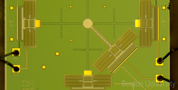
A Dec. 29, 2015 DARPA news release, which originated the news item, offers more information and an image illustrating the type of advances already made by one of the successful proponents,

DARPA recently launched its Atoms to Product (A2P) program, with the goal of developing technologies and processes to assemble nanometer-scale pieces—whose dimensions are near the size of atoms—into systems, components, or materials that are at least millimeter-scale in size. At the heart of that goal was a frustrating reality: Many common materials, when fabricated at nanometer-scale, exhibit unique and attractive “atomic-scale” behaviors including quantized current-voltage behavior, dramatically lower melting points and significantly higher specific heats—but they tend to lose these potentially beneficial traits when they are manufactured at larger “product-scale” dimensions, typically on the order of a few centimeters, for integration into devices and systems.

“The ability to assemble atomic-scale pieces into practical components and products is the key to unlocking the full potential of micromachines,” said John Main, DARPA program manager. “The DARPA Atoms to Product Program aims to bring the benefits of microelectronic-style miniaturization to systems and products that combine mechanical, electrical, and chemical processes.”

The program calls for closing the assembly gap in two steps: From atoms to microns and from microns to millimeters. Performers are tasked with addressing one or both of these steps and have been assigned to one of three working groups, each with a distinct focus area.

A2P

Image caption: Microscopic tools such as this nanoscale “atom writer” can be used to fabricate minuscule light-manipulating structures on surfaces. DARPA has selected 10 performers for its Atoms to Product (A2P) program whose goal is to develop technologies and processes to assemble nanometer-scale pieces—whose dimensions are near the size of atoms—into systems, components, or materials that are at least millimeter-scale in size. (Image credit: Boston University)

Here’s more about the projects and the performers (proponents) from the A2P performers page on the DARPA website,

Nanometer to Millimeter in a Single System – Embody, Draper and Voxtel

Current methods to treat ligament injuries in warfighters [also known as, soldiers]—which account for a significant portion of reported injuries—often fail to restore pre-injury performance, due to surgical complexities and an inadequate supply of donor tissue. Embody is developing reinforced collagen nanofibers that mimic natural ligaments and replicate the biological and biomechanical properties of native tissue. Embody aims to create a new standard of care and restore pre-injury performance for warfighters and sports injury patients at a 50% reduction compared to current costs.

Radio Frequency (RF) systems (e.g., cell phones, GPS) have performance limits due to alternating current loss. In lower frequency power systems this is addressed by braiding the wires, but this is not currently possibly in cell phones due to an inability to manufacture sufficiently small braided wires. Draper is developing submicron wires that can be braided using DNA self-assembly methods. If successful, portable RF systems will be more power efficient and able to send 10 times more information in a given channel.

For seamless control of structures, physics and surface chemistry—from the atomic-level to the meter-level—Voxtel Inc. and partner Oregon State University are developing an efficient, high-rate, fluid-based manufacturing process designed to imitate nature’s ability to manufacture complex multimaterial products across scales. Historically, challenges relating to the cost of atomic-level control, production speed, and printing capability have been effectively insurmountable. This team’s new process will combine synthesis and delivery of materials into a massively parallel inkjet operation that draws from nature to achieve a DNA-like mediated assembly. The goal is to assemble complex, 3-D multimaterial mixed organic and inorganic products quickly and cost-effectively—directly from atoms.

Optical Metamaterial Assembly – Boston University, University of Notre Dame, HRL and PARC.

Nanoscale devices have demonstrated nearly unlimited power and functionality, but there hasn’t been a general- purpose, high-volume, low-cost method for building them. Boston University is developing an atomic calligraphy technique that can spray paint atoms with nanometer precision to build tunable optical metamaterials for the photonic battlefield. If successful, this capability could enhance the survivability of a wide range of military platforms, providing advanced camouflage and other optical illusions in the visual range much as stealth technology has enabled in the radar range.

The University of Notre Dame is developing massively parallel nanomanufacturing strategies to overcome the requirement today that most optical metamaterials must be fabricated in “one-off” operations. The Notre Dame project aims to design and build optical metamaterials that can be reconfigured to rapidly provide on-demand, customized optical capabilities. The aim is to use holographic traps to produce optical “tiles” that can be assembled into a myriad of functional forms and further customized by single-atom electrochemistry. Integrating these materials on surfaces and within devices could provide both warfighters and platforms with transformational survivability.

HRL Laboratories is working on a fast, scalable and material-agnostic process for improving infrared (IR) reflectivity of materials. Current IR-reflective materials have limited use, because reflectivity is highly dependent on the specific angle at which light hits the material. HRL is developing a technique for allowing tailorable infrared reflectivity across a variety of materials. If successful, the process will enable manufacturable materials with up to 98% IR reflectivity at all incident angles.

PARC is working on building the first digital MicroAssembly Printer, where the “inks” are micrometer-size particles and the “image” outputs are centimeter-scale and larger assemblies. The goal is to print smart materials with the throughput and cost of laser printers, but with the precision and functionality of nanotechnology. If successful, the printer would enable the short-run production of large, engineered, customized microstructures, such as metamaterials with unique responses for secure communications, surveillance and electronic warfare.

Flexible, General Purpose Assembly – Zyvex, SRI, and Harvard.

Zyvex aims to create nano-functional micron-scale devices using customizable and scalable manufacturing that is top-down and atomically precise. These high-performance electronic, optical, and nano-mechanical components would be assembled by SRI micro-robots into fully-functional devices and sub-systems such as ultra-sensitive sensors for threat detection, quantum communication devices, and atomic clocks the size of a grain of sand.

SRI’s Levitated Microfactories will seek to combine the precision of MEMS [micro-electromechanical systems] flexures with the versatility and range of pick-and-place robots and the scalability of swarms [an idea Michael Crichton used in his 2002 novel Prey to induce horror] to assemble and electrically connect micron and millimeter components to build stronger materials, faster electronics, and better sensors.

Many high-impact, minimally invasive surgical techniques are currently performed only by elite surgeons due to the lack of tactile feedback at such small scales relative to what is experienced during conventional surgical procedures. Harvard is developing a new manufacturing paradigm for millimeter-scale surgical tools using low-cost 2D layer-by-layer processes and assembly by folding, resulting in arbitrarily complex meso-scale 3D devices. The goal is for these novel tools to restore the necessary tactile feedback and thereby nurture a new degree of dexterity to perform otherwise demanding micro- and minimally invasive surgeries, and thus expand the availability of life-saving procedures.

Sidebar

‘Sidebar’ is my way of indicating these comments have little to do with the matter at hand but could be interesting factoids for you.

First, Zyvex Labs was last mentioned here in a Sept. 10, 2014 posting titled: OCSiAL will not be acquiring Zyvex. Notice that this  announcement was made shortly after DARPA’s A2P program was announced and that OCSiAL is one of RUSNANO’s (a Russian funding agency focused on nanotechnology) portfolio companies (see my Oct. 23, 2015 posting for more).

HRL Laboratories, mentioned here in an April 19, 2012 posting mostly concerned with memristors (nanoscale devices that mimic neural or synaptic plasticity), has its roots in Howard Hughes’s research laboratories as noted in the posting. In 2012, HRL was involved in another DARPA project, SyNAPSE.

Finally and minimally, PARC also known as, Xerox PARC, was made famous by Steven Jobs and Steve Wozniak when they set up their own company (Apple) basing their products on innovations that PARC had rejected. There are other versions of the story and one by Malcolm Gladwell for the New Yorker May 16, 2011 issue which presents a more complicated and, at times, contradictory version of that particular ‘origins’ story.

Bioceramic armour: tough and clear

This story about a mollusk and its armour eventually led me back to one of my favourite science writers, David L. Chandler at the Massachusetts Institute of Technology (MIT). First, here’s an excerpt from a March 30, 2014 news item on ScienceDaily,

The shells of a sea creature, the mollusk Placuna placenta, are not only exceptionally tough, but also clear enough to read through. Now, researchers at MIT have analyzed these shells to determine exactly why they are so resistant to penetration and damage — even though they are 99 percent calcite, a weak, brittle mineral.

The shells’ unique properties emerge from a specialized nanostructure that allows optical clarity, as well as efficient energy dissipation and the ability to localize deformation, the researchers found. The results are published this week in the journal Nature Materials, in a paper co-authored by MIT graduate student Ling Li and professor Christine Ortiz.

A March 30, 2014 MIT press release (I’m not positive Chandler wrote this but he is the press contact) describes both the engineered bioceramic armour and the mollusk’s naturally occurring armour,

Engineered ceramic-based armor, while designed to resist penetration, often lacks the ability to withstand multiple blows, due to large-scale deformation and fracture that can compromise its structural integrity, Ortiz says. In transparent armor systems, such deformation can also obscure visibility.

Creatures that have evolved natural exoskeletons — many of them ceramic-based — have developed ingenious designs that can withstand multiple penetrating attacks from predators. The shells of a few species, such as Placuna placenta, are also optically clear.

To test exactly how the shells — which combine calcite with about 1 percent organic material — respond to penetration, the researchers subjected samples to indentation tests, using a sharp diamond tip in an experimental setup that could measure loads precisely. They then used high-resolution analysis methods, such as electron microscopy and diffraction, to examine the resulting damage.

The material initially isolates damage through an atomic-level process called “twinning” within the individual ceramic building blocks: A crystal breaks up into a pair of mirror-image regions that share a common boundary, rather like a butterfly’s wings. This twinning process occurs all around the stressed region, helping to form a kind of boundary that keeps the damage from spreading outward.

The MIT researchers found that twinning then activates “a series of additional energy-dissipation mechanisms … which preserve the mechanical and optical integrity of the surrounding material,” Li says. This produces a material that is 10 times more efficient in dissipating energy than the pure mineral, Li adds.

The properties of this natural armor make it a promising template for the development of bio-inspired synthetic materials for both commercial and military applications — such as eye and face protection for soldiers, windows and windshields, and blast shields, Ortiz says.

Huajian Gao, a professor of engineering at Brown University who was not involved in this research, calls it “an excellent and elegant piece of work.” He says it “successfully demonstrates the effectiveness of nanoscale deformation twins in energy dissipation in bioceramics, and should be able to inspire and guide the development of manmade ceramic materials.” He adds, “As a first-of-its-kind [demonstration of] the effectiveness of deformation twins in natural materials, this work should have huge practical impact.”

The work was supported by the National Science Foundation; the U.S. Army Research Office through the MIT Institute for Soldier Nanotechnologies; the National Security Science and Engineering Faculty Fellowships Program; and the Office of the Assistant Secretary of Defense for Research and Engineering.

The researchers have produced an image showing how the mollusk shell reacts to being damaged,

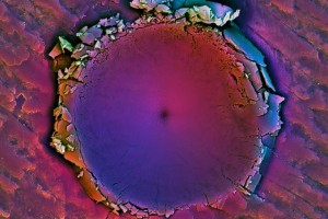
A Scanning Electron Microscope (SEM) image of the region surrounding an indentation the researchers made in a piece of shell from Placuna placenta. The image shows the localization of damage to the area immediately surrounding the stress. Image: Ling Li and James C. Weaver. Courtesy: MIT

A Scanning Electron Microscope (SEM) image of the region surrounding an indentation the researchers made in a piece of shell from Placuna placenta. The image shows the localization of damage to the area immediately surrounding the stress.
Image: Ling Li and James C. Weaver. Courtesy: MIT

Here’s a link to and a citation for the paper,

Pervasive nanoscale deformation twinning as a catalyst for efficient energy dissipation in a bioceramic armour by Ling Li & Christine Ortiz. Nature Materials (2014) doi:10.1038/nmat3920 Published online 30 March 2014

This paper is behind a paywall.

Snow reveals the truth about crystalline growth

A Jan. 24, 2014 news item on Nanowerk has a beautiful and timely (given the snowy, frigid weather in Eastern Canada and the US) opening for a story about crystals and metallic nanorods,

This time of year it’s not hard to imagine the world buried under a smooth blanket of snow. A picnic table on a flat lawn eventually vanishes as trillions of snowflakes collect around it, a crystalline sheet obscuring the normall – visible peaks and valleys of our summertime world.

This is basically how scientists understand the classical theory of crystalline growth. Height steps gradually disappear as atoms of a given material—be it snow or copper or aluminum—collect on a surface and then tumble down to lower heights to fill in the gaps. The only problem with this theory is that it totally falls apart when applied to extremely small situations—i.e., the nanoscale.

The Jan. 23, 2014 Northeastern University news release by Angela Herring, which originated the news item, goes on to provide some context and describe this work concerning nanorods,

Hanchen Huang, pro­fessor and chair of the Depart­ment of Mechan­ical and Indus­trial Engi­neering [Northeastern University located in Massachusetts, US], has spent the last 10 years revising the clas­sical theory of crystal growth that accounts for his obser­va­tions of nanorod crys­tals. His work has gar­nered the con­tinued sup­port of the U.S, Depart­ment of Energy’s Basic Energy Sci­ence Core Program.

Nanorods are minis­cule fibers grown per­pen­dic­ular to a sub­strate, each one about 100,000 times thinner than a human hair. Sur­face steps, or the minor vari­a­tions in the ver­tical land­scape of that sub­strate, deter­mine how the rods will grow.

“Even if some sur­face steps are closer and others more apart at the start, with time the clas­sical theory pre­dicts they become more equal­ized,” Huang said. “But we found that the clas­sical theory missed a pos­i­tive feed­back mechanism.”

This mech­a­nism, he explained, causes the steps to “cluster,” making it more dif­fi­cult for atoms to fall from a higher step to a lower one. So, instead of filling in the height gaps of a vari­able sur­face, atoms in a nanorod crystal localize to the highest levels.

“The taller region gets taller,” Huang said. “It’s like, if you ever play bas­ket­ball, you know the taller guys will get more rebounds.” That’s basi­cally what hap­pens with nanorod growth.

Huang’s theory, which was pub­lished in the journal Phys­ical Review Let­ters this year, rep­re­sents the first time anyone has pro­vided a the­o­ret­ical frame­work for under­standing nanorod crystal growth. “Lots of money has been spent over the past decades on nanoscience and nan­otech­nology,” Huang said. “But we can only turn that into real-​​world appli­ca­tions if we under­stand the science.”

Indeed, his con­tri­bu­tion to under­standing the sci­ence allowed him and his col­leagues to pre­dict the smallest pos­sible size for copper nanorods and then suc­cess­fully syn­the­size them. Not only are they the smallest nanorods ever pro­duced, but with Huang’s theory he can con­fi­dently say they are the smallest nanorods pos­sible using phys­ical vapor deposition.

Here’s a link to and a citation for the paper,

Smallest Metallic Nanorods Using Physical Vapor Deposition by Xiaobin Niu, Stephen P. Stagon, Hanchen Huang, J. Kevin Baldwin, and Amit Misra. Phys. Rev. Lett. 110 (no. 13), 136102 (2013) [5 pages] DoI:
10.1103/PhysRevLett.110.136102

This paper is behind a paywall.

Nature imitates art at Northeastern University (US)

It’s an intriguing mental exercise trying to flip the tables on nature as an inspiration for art to start discussing ‘artmimetics’ as they seem to be doing at Northeastern University (Boston, Massachusetts, US), according to a Dec. 11, 2013 news item on Azonano,

There are exam­ples of art imi­tating nature all around us—whether it’s Monet’s pastel Water Lilies or Chihuly’s glass­blown Seaforms, the human con­cep­tion of nat­ural phe­nomena daz­zles but does not often surprise.

Yet when asso­ciate pro­fessor of physics Latika Menon peered under the elec­tron micro­scope last fall, she dis­cov­ered the exact oppo­site. Instead of art imi­tating nature, she found nature imi­tating art.

The Dec. 10, 2013 Northeastern University news release by Angela Herring, which ‘inspired’ the news item, describes how Menon and her colleagues came to reverse the inspirational direction,

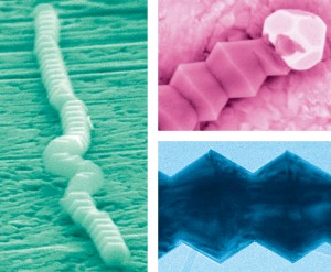
Menon grew up in the eastern region of India and was vaguely familiar with a cul­tural dance from the western state of Rajasthan known as the Bhavai pot dance. Nimble dancers sway their hips as a tall stack of wide-​​bellied pots bal­ances gin­gerly atop their heads. Back in the lab at North­eastern, Menon’s team recently cre­ated  gal­lium nitride nanowires, which bore a striking resem­blance to that stack of pots.

What’s more, a post­doc­toral research asso­ciate in Menon’s lab, Eugen Panaitescu, jumped on the band­wagon with a cul­tural art ref­er­ence of his own. Panaitescu, who hails from Romania, also saw his country’s famous End­less Column reflected in the nanowires. Ded­i­cated to the fallen Romanian heroes of World War I, Con­stantin Brancusi’s 96-​​foot-​​tall mono­lith is con­structed of 17 three-​​dimensional rhom­buses, peri­od­i­cally wavering from a wider cir­cum­fer­ence to a nar­rower one.

The news release goes on to explain more about applications using gallium nitride and why Menon’s insight may prove useful in developing new uses for gallium nitride nanowires,

… Gal­lium nitride is used across a range of tech­nolo­gies, including most ubiq­ui­tously in light emit­ting diodes. The mate­rial also holds great poten­tial for solar cell arrays, mag­netic semi­con­duc­tors, high-​​frequency com­mu­ni­ca­tion devices, and many other things. But these advanced appli­ca­tions are restricted by our lim­ited ability to con­trol the material’s growth on the nanoscale.

The very thing that makes Menon’s nanowires beau­tiful rep­re­sents a break­through in her ability to process them for these novel uses. She deposited onto a sil­icon sub­strate small droplets of liquid gold metal, which act as cat­a­lysts to grab gaseous gal­lium nitride from the atmos­phere of the exper­i­mental system. The net forces between the tiny gold droplet, the solid sub­strate, and the gas cause the nanowire to grow in a par­tic­ular direc­tion, she explained. Depending on the size of the gold cat­a­lyst, she can create wires that exhibit peri­odic serrations.

“It first tries to grow out­ward, but that gives the gold a larger sur­face area,” she said. “So now the wire gets pulled in the inward direc­tion, and then the gold gets a smaller sur­face area, so it grows out­ward again.” This inward and out­ward growth repeated itself again and again to create a peri­odic struc­ture nearly 6 mil­lion times smaller than the end­less column and is sig­nif­i­cantly more promising for its use in advanced devices.

“That there is very little imple­men­ta­tion of nanowire tech­nology in elec­tronics or optical devices is due to the fact that it’s very hard to con­trol their shape and dimen­sions,” said Menon. But now that she has a very simple way of con­trol­ling growth, the next step is to con­trol the size of the cat­alytic droplet with which she starts.

Another advan­tage of Menon’s approach is using what Panaitescu called “macro­scopic tech­niques” to create nanoscale mate­rials, thus making it scal­able and inex­pen­sive. “We just con­trol a few para­me­ters and then leave it, let it do it’s nat­ural thing,” explained Menon.

Here’s an image the researchers have supplied to illustrate their insights and their work,

Depending on the size of the gold cat­a­lyst used to make them, Latika Menon’s nanowires will exhibit peri­odic grooves that resemble common motifs in art. Images cour­tesy of Latika Menon. - See more at: http://www.northeastern.edu/news/2013/12/menon-nanowires/#sthash.LkgJU4es.dpuf

Depending on the size of the gold cat­a­lyst used to make them, Latika Menon’s nanowires will exhibit peri­odic grooves that resemble common motifs in art. Images cour­tesy of Latika Menon. – See more at: http://www.northeastern.edu/news/2013/12/menon-nanowires/#sthash.LkgJU4es.dpuf

I’m not sure I can connect the  imagery in this pot dance video (it does show some pretty astonishing feats of balance) with any of the images from Menon’s lab but sometimes the source of an inspiration is not readily accessible to those who are not amongst the inspired or perhaps there other versions of the dance that make it more obvious to an untrained eye,

Here’s an image of the other artistic inspiration, Constantin Brancusi’s Endless Column found on Dr. Cătălina Köpetz’s (University of Maryland) webpage featuring Brancusi’s work along with this quote from him “Create like a god, comand like a king, work like a slave.”

The Endless Column, Târgu Jiu, România  [downlaoded from http://terpconnect.umd.edu/~ckopetz/brancusi.htm]

The Endless Column,
Târgu Jiu, România [downlaoded from http://terpconnect.umd.edu/~ckopetz/brancusi.htm]

Interestingly, Dr. Köpetz is a social psychologist working in the university’s Center for Addictions, Personality, and Emotion Research.

For anyone who’d like to read more about Menon’s work, here’s a link to a webpage featuring a PDF selection of her papers and a citation for her latest paper on the work described in the news release,

Vapor–liquid–solid growth of serrated GaN nanowires: shape selection driven by kinetic frustration by Zheng Ma, Dillon McDowell, Eugen Panaitescu, Albert V. Davydov, Moneesh Upmanyu and Latika Menon, Physics Faculty Publications (2013)

Compound semiconducting nanowires are promising building blocks for several nanoelectronic devices yet the inability to…

The paper is open access although you will have to click a few times to retrieve it.