Tag Archives: metal nanoparticles

Metals useful in photonics?

Researchers at the University of Ottawa have debunked a myth, one involving metals and light according to a March 1i, 2021 news item on phys.org (Note: Links have been removed),

Researchers at the University of Ottawa have debunked the decade-old myth of metals being useless in photonics—the science and technology of light—with their findings, recently published in Nature Communications, expected to lead to many applications in the field of nanophotonics.

“We broke the record for the resonance quality factor (Q-factor) of a periodic array of metal nanoparticles by one order of magnitude compared to previous reports,” said senior author Dr. Ksenia Dolgaleva, Canada Research Chair in Integrated Photonics (Tier 2) and Associate Professor in the School of Electrical Engineering and Computer Science (EECS) at the University of Ottawa.

A March 18, 2021 University of Ottawa news release (also on EurekAlert), which originated the news item, introduced me to the word ‘lossy’ and discussed the decade-long myth in more detail,

“It is a well-known fact that metals are very lossy when they interact with light, which means they cause the dissipation of electrical energy. The high losses compromise their use in optics and photonics. We demonstrated ultra-high-Q resonances in a metasurface (an artificially structured surface) comprised of an array of metal nanoparticles embedded inside a flat glass substrate. These resonances can be used for efficient light manipulating and enhanced light-matter interaction, showing metals are useful in photonics.”

“In previous works, researchers attempted to mitigate the adverse effect of losses to access favorable properties of metal nanoparticle arrays,” observed the co-lead author of the study Md Saad Bin-Alam, a uOttawa doctoral student in EECS.

“However, their attempts did not provide a significant improvement in the quality factors of the resonances of the arrays. We implemented a combination of techniques rather than a single approach and obtained an order-of-magnitude improvement demonstrating a metal nanoparticle array (metasurface) with a record-high quality factor.”

According to the researchers, structured surfaces – also called metasurfaces – have very promising prospects in a variety of nanophotonic applications that can never be explored using traditional natural bulk materials. Sensors, nanolasers, light beam shaping and steering are just a few examples of the many applications.

“Metasurfaces made of noble metal nanoparticles – gold or silver for instance – possess some unique benefits over non-metallic nanoparticles. They can confine and control light in a nanoscale volume that is less than one quarter of the wavelength of light (less than 100 nm, while the width of a hair is over 10 000 nm),” explained Md Saad Bin-Alam.

“Interestingly, unlike in non-metallic nanoparticles, the light is not confined or trapped inside the metal nanoparticles but is concentrated close to their surface. This phenomenon is scientifically called ‘localized surface plasmon resonances (LSPRs)’. This feature gives a great superiority to metal nanoparticles compared to their dielectric counterparts, because one could exploit such surface resonances to detect bio-organisms or molecules in medicine or chemistry. Also, such surface resonances could be used as the feedback mechanism necessary for laser gain. In such a way, one can realize a nanoscale tiny laser that can be adopted in many future nanophotonic applications, like light detection and ranging (LiDAR) for the far-field object detection.”

According to the researchers, the efficiency of these applications depends on the resonant Q-factors.

“Unfortunately, due to the high ‘absorptive’ and ‘radiative’ loss in metal nanoparticles, the LSPRs Q-factors are very low,” said co-lead author Dr. Orad Reshef, a postdoctoral fellow in the Department of Physics at the University of Ottawa.

“More than a decade ago, researchers found a way to mitigate the dissipative loss by carefully arranging the nanoparticles in a lattice. From such ‘surface lattice’ manipulation, a new ‘surface lattice resonance (SLR)’ emerges with suppressed losses. Until our work, the maximum Q-factors reported in SLRs was around a few hundred. Although such early reported SLRs were better than the low-Q LSPRs, they were still not very impressive for efficient applications. It led to the myth that metals are not useful for practical applications.”

A myth that the group was able to deconstruct during its work at the University of Ottawa’s Advanced Research Complex between 2017 and 2020.

“At first, we performed numerical modelling of a gold nanoparticle metasurface and were surprised to obtain quality factors of several thousand,” said Md Saad Bin-Alam, who primarily designed the metasurface structure.

“This value has never been reported experimentally, and we decided to analyze why and to attempt an experimental demonstration of such a high Q. We observed a very high-Q SLR of value nearly 2400, that is at least 10 times larger than the largest SLRs Q reported earlier.”

A discovery that made them realize that there’s still a lot to learn about metals.

“Our research proved that we are still far from knowing all the hidden mysteries of metal (plasmonic) nanostructures,” concluded Dr. Orad Reshef, who fabricated the metasurface sample. “Our work has debunked a decade-long myth that such structures are not suitable for real-life optical applications due to the high losses. We demonstrated that, by properly engineering the nanostructure and carefully conducting an experiment, one can improve the result significantly.”

Here’s a link to and a citation for the paper,

Ultra-high-Q resonances in plasmonic metasurfaces by M. Saad Bin-Alam, Orad Reshef, Yaryna Mamchur, M. Zahirul Alam, Graham Carlow, Jeremy Upham, Brian T. Sullivan, Jean-Michel Ménard, Mikko J. Huttunen, Robert W. Boyd & Ksenia Dolgaleva. Nature Communications volume 12, Article number: 974 (2021) DOI: https://doi.org/10.1038/s41467-021-21196-2 Published 12 February 2021

This paper is open access.

Spinning gold out of nanocellulose

If you’re hoping for a Rumpelstiltskin reference (there is more about the fairy tale at the end of this posting) and despite the press release’s headline, you won’t find it in this August 10, 2020 news item on Nanowerk,

When nanocellulose is combined with various types of metal nanoparticles, materials are formed with many new and exciting properties. They may be antibacterial, change colour under pressure, or convert light to heat.

“To put it simply, we make gold from nanocellulose”, says Daniel Aili, associate professor in the Division of Biophysics and Bioengineering at the Department of Physics, Chemistry and Biology at Linköping University.

The research group, led by Daniel Aili, has used a biosynthetic nanocellulose produced by bacteria and originally developed for wound care. The scientists have subsequently decorated the cellulose with metal nanoparticles, principally silver and gold. The particles, no larger than a few billionths of a metre, are first tailored to give them the properties desired, and then combined with the nanocellulose.

An August 10, 2020 Linköping University press release (also on EurekAlert), which originated the news item,expands on a few details about the work (sob … without mentioning Rumpelstiltskin),

“Nanocellulose consists of thin threads of cellulose, with a diameter approximately one thousandth of the diameter of a human hair. The threads act as a three-dimensional scaffold for the metal particles. When the particles attach themselves to the cellulose, a material that consists of a network of particles and cellulose forms”, Daniel Aili explains.

The researchers can determine with high precision how many particles will attach, and their identities. They can also mix particles of different metals and with different shapes – spherical, elliptical and triangular.

In the first part of a scientific article published in Advanced Functional Materials, the group describes the process and explains why it works as it does. The second part focusses on several areas of application.

One exciting phenomenon is the way in which the properties of the material change when pressure is applied. Optical phenomena arise when the particles approach each other and interact, and the material changes colour. As the pressure increases, the material eventually appears to be gold.

“We saw that the material changed colour when we picked it up in tweezers, and at first we couldn’t understand why”, says Daniel Aili.

The scientists have named the phenomenon “the mechanoplasmonic effect”, and it has turned out to be very useful. A closely related application is in sensors, since it is possible to read the sensor with the naked eye. An example: If a protein sticks to the material, it no longer changes colour when placed under pressure. If the protein is a marker for a particular disease, the failure to change colour can be used in diagnosis. If the material changes colour, the marker protein is not present.

Another interesting phenomenon is displayed by a variant of the material that absorbs light from a much broader spectrum visible light and generates heat. This property can be used for both energy-based applications and in medicine.

“Our method makes it possible to manufacture composites of nanocellulose and metal nanoparticles that are soft and biocompatible materials for optical, catalytic, electrical and biomedical applications. Since the material is self-assembling, we can produce complex materials with completely new well-defined properties,” Daniel Aili concludes.

Here’s a link to and a citation for the paper,

Self‐Assembly of Mechanoplasmonic Bacterial Cellulose–Metal Nanoparticle Composites by Olof Eskilson, Stefan B. Lindström, Borja Sepulveda, Mohammad M. Shahjamali, Pau Güell‐Grau, Petter Sivlér, Mårten Skog, Christopher Aronsson, Emma M. Björk, Niklas Nyberg, Hazem Khalaf, Torbjörn Bengtsson, Jeemol James, Marica B. Ericson, Erik Martinsson, Robert Selegård, Daniel Aili. Advanced Functional Materials DOI: https://doi.org/10.1002/adfm.202004766 First published: 09 August 2020

This paper is open access.

As for Rumpelstiltskin, there’s this abut the story’s origins and its cross-cultural occurrence, from its Wikipedia entry,

“Rumpelstiltskin” (/ˌrʌmpəlˈstɪltskɪn/ RUMP-əl-STILT-skin[1]) is a fairy tale popularly associated with Germany (where it is known as Rumpelstilzchen). The tale was one collected by the Brothers Grimm in the 1812 edition of Children’s and Household Tales. According to researchers at Durham University and the NOVA University Lisbon, the story originated around 4,000 years ago.[2][3] However, many biases led some to take the results of this study with caution.[4]

The same story pattern appears in numerous other cultures: Tom Tit Tot in England (from English Fairy Tales, 1890, by Joseph Jacobs); The Lazy Beauty and her Aunts in Ireland (from The Fireside Stories of Ireland, 1870 by Patrick Kennedy); Whuppity Stoorie in Scotland (from Robert Chambers’s Popular Rhymes of Scotland, 1826); Gilitrutt in Iceland; جعيدان (Joaidane “He who talks too much”) in Arabic; Хламушка (Khlamushka “Junker”) in Russia; Rumplcimprcampr, Rampelník or Martin Zvonek in the Czech Republic; Martinko Klingáč in Slovakia; “Cvilidreta” in Croatia; Ruidoquedito (“Little noise”) in South America; Pancimanci in Hungary (from A Csodafurulya, 1955, by Emil Kolozsvári Grandpierre, based on the 19th century folktale collection by László Arany); Daiku to Oniroku (大工と鬼六 “A carpenter and the ogre”) in Japan and Myrmidon in France.

An earlier literary variant in French was penned by Mme. L’Héritier, titled Ricdin-Ricdon.[5] A version of it exists in the compilation Le Cabinet des Fées, Vol. XII. pp. 125-131.

The Cornish tale of Duffy and the Devil plays out an essentially similar plot featuring a “devil” named Terry-top.

All these tales are Aarne–Thompson type 500, “The Name of the Helper”.[6]

Should you be curious about the story as told by the Brothers Grimm, here’s the beginning to get you started (from the grimmstories.com Rumpelstiltskin webpage),

There was once a miller who was poor, but he had one beautiful daughter. It happened one day that he came to speak with the king, and, to give himself consequence, he told him that he had a daughter who could spin gold out of straw. The king said to the miller: “That is an art that pleases me well; if thy daughter is as clever as you say, bring her to my castle to-morrow, that I may put her to the proof.”

When the girl was brought to him, he led her into a room that was quite full of straw, and gave her a wheel and spindle, and said: “Now set to work, and if by the early morning thou hast not spun this straw to gold thou shalt die.” And he shut the door himself, and left her there alone. And so the poor miller’s daughter was left there sitting, and could not think what to do for her life: she had no notion how to set to work to spin gold from straw, and her distress grew so great that she began to weep. Then all at once the door opened, and in came a little man, who said: “Good evening, miller’s daughter; why are you crying?”

Enjoy! BTW, should you care to, you can find three other postings here tagged with ‘Rumpelstiltskin’. I think turning dross into gold is a popular theme in applied science.

Nanoparticles in combination could be more toxic

It seems that one set of nanoparticles, e.g., silver nanoparticles, in combination with another material, e.g., cadmium ions, are more dangerous than either one separately according to an August 17, 2018 University of Southern Denmark press release by Birgitte Svennevig (also on EurekAlert but dated August 20, 2018),

Researchers warn that a combination of nanoparticles and contaminants may form a cocktail that is harmful to our cells. In their study, 72 pct. of cells died after exposure to a cocktail of nano-silver and cadmium ions.

Nanoparticles are becoming increasingly widespread in our environment. Thousands of products contain nanoparticles because of their unique properties. Silver nanoparticles are one example: They have an effective antibacterial effect and can be found in refrigerators, sports clothes, cosmetics, tooth brushes, water filters, etc.

There is a significant difference between how the cells react when exposed to nanosilver alone and when they are exposed to a cocktail of nanosilver and cadmium ions. Cadmium ions are naturally found everywhere around us on Earth.

In the study, 72 pct. of the cells died, when exposed to both nanosilver and cadmiun ions. When exposed to nanosilver only, 25 pct. died. When exposed to cadmium ions only, 12 pct. died.

The study was conducted on human liver cancer cells.

  • This study indicates, that we should not look at nanoparticles isolated when we investigate and discuss the effects, they may have on our health. We need to take cocktail effects into account, said Professor Frank Kjeldsen, Dept of Biochemistry and Molecular Biology, SDU, adding:
  • Products with nano particles are being developed and manufactured every day, but in most countries there are no regulations, so there is no way of knowing what and how many nanoparticles are being released into the environment. In my opinion, this should be stopped.

Other studies, led by Professor Kjeldsen have previously shown that human cells interact with metal nanoparticles.

One study showed that nano-silver leads to the formation free radicals in cells and changes in the form and amount of proteins. Many serious diseases are characterized by an overproduction of free radicals in cells. This applies to cancer and neurological diseases such as Alzheimer’s and Parkinson’s.

This is not great news but there are a few things to note about this research. First, it was conducted on cells and therefore not subject to some of the defensive systems found in complete biological organisms such as a mouse or a dandelion plant for example.

Also, since they were cancer cells one might suspect their reactions might differ from those of healthy cells. As for how the cells were exposed to the contaminants, I think (???) they were sitting in a solution of contaminants and most of us do not live in that kind of environment.. Finally, with regard to the concentrations, I have no idea if they are greater than one might expect to encounter in one’s lifecycle but it’s always worth questioning just how much exposure you might expect during yours or a mouse’s or a dandelion’s life.

These caveats aside, Professor Frank Kjeldsen’s work raises some very concerning issues and his work adds to a growing body of evidence.

Here’s a video featuring Dr. Kjeldsen talking about his work,

Here’s a link to and a citation for the paper,

Co-exposure to silver nanoparticles and cadmium induce metabolic adaptation in HepG2 cells by Renata Rank Miranda, Vladimir Gorshkov, Barbara Korzeniowska, Stefan J. Kempf, Francisco Filipak Neto, & Frank Kjeldsen. Nanotoxicology DOI: https://doi.org/10.1080/17435390.2018.1489987 Published online: 11 Jul 2018

This paper is open access.

Colo(u)r-changing nanolaser inspired by chameleons

Caption: Novel nanolaser leverages the same color-changing mechanism that a chameleon uses to camouflage its skin. Credit: Egor Kamelev Courtesy: Northwestern University

I wish there was some detail included about how those colo(u)rs were achieved in that photograph. Strangely, Northwestern University (Chicago, Illinois, US) is more interested in describing the technology that chameleons have inspired. A June 20, 2018 news item on ScienceDaily announces the research,

As a chameleon shifts its color from turquoise to pink to orange to green, nature’s design principles are at play. Complex nano-mechanics are quietly and effortlessly working to camouflage the lizard’s skin to match its environment.

Inspired by nature, a Northwestern University team has developed a novel nanolaser that changes colors using the same mechanism as chameleons. The work could open the door for advances in flexible optical displays in smartphones and televisions, wearable photonic devices and ultra-sensitive sensors that measure strain.

A June 20, 2018 Northwestern University news release (also on EurekAlert) by Amanda Morris, which originated the news item, expands on the theme,

“Chameleons can easily change their colors by controlling the spacing among the nanocrystals on their skin, which determines the color we observe,” said Teri W. Odom, Charles E. and Emma H. Morrison Professor of Chemistry in Northwestern’s Weinberg College of Arts and Sciences. “This coloring based on surface structure is chemically stable and robust.”

The research was published online yesterday [June 19, 2018] in the journal Nano Letters. Odom, who is the associate director of Northwestern’s International Institute of Nanotechnology, and George C. Schatz, Charles E. and Emma H. Morrison Professor of Chemistry in Weinberg, served as the paper’s co-corresponding authors.

The same way a chameleon controls the spacing of nanocrystals on its skin, the Northwestern team’s laser exploits periodic arrays of metal nanoparticles on a stretchable, polymer matrix. As the matrix either stretches to pull the nanoparticles farther apart or contracts to push them closer together, the wavelength emitted from the laser changes wavelength, which also changes its color.

“Hence, by stretching and releasing the elastomer substrate, we could select the emission color at will,” Odom said.

The resulting laser is robust, tunable, reversible and has a high sensitivity to strain. These properties are critical for applications in responsive optical displays, on-chip photonic circuits and multiplexed optical communication.

Here’s a link to and a citation for the paper,

Stretchable Nanolasing from Hybrid Quadrupole Plasmons by Danqing Wang, Marc R. Bourgeois, Won-Kyu Lee, Ran Li, Dhara Trivedi, Michael P. Knudson, Weijia Wang, George C. Schatz, and Teri W. Odom. Nano Lett., Article ASAP DOI: 10.1021/acs.nanolett.8b01774 Publication Date (Web): June 18, 2018

Copyright © 2018 American Chemical Society

This paper is behind a paywall.

Building metal nanoparticles: one step closer

University of Pittsburgh scientists have researched why metal nanoparticles form, a necessary first step before developing techniques for synthesizing them commercially. From a July 10, 2017 news item on ScienceDaily,

Although scientists have for decades been able to synthesize nanoparticles in the lab, the process is mostly trial and error, and how the formation actually takes place is obscure. A new study explains how metal nanoparticles form.

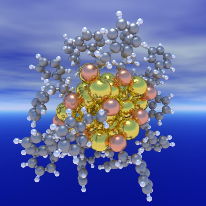
Caption: This is a structure of a ligand-protected Au25 nanocluster. Credit: Computer-Aided Nano and Energy Lab (C.A.N.E.LA.)

A July 10, 2017 University of Pittsburgh news release (also on EurekAlert), which originated the news item, expands on the theme (Note: A link has been removed),

“Even though there is extensive research into metal nanoparticle synthesis, there really isn’t a rational explanation why a nanoparticle is formed,” Dr. Mpourmpakis [Giannis Mpourmpakis, assistant professor of chemical and petroleum engineering] said. “We wanted to investigate not just the catalytic applications of nanoparticles, but to make a step further and understand nanoparticle stability and formation. This new thermodynamic stability theory explains why ligand-protected metal nanoclusters are stabilized at specific sizes.”

A ligand is a molecule that binds to metal atoms to form metal cores that are stabilized by a shell of ligands, and so understanding how they contribute to nanoparticle stabilization is essential to any process of nanoparticle application. Dr. Mpourmpakis explained that previous theories describing why nanoclusters stabilized at specific sizes were based on empirical electron counting rules – the number of electrons that form a closed shell electronic structure, but show limitations since there have been metal nanoclusters experimentally synthesized that do not necessarily follow these rules.

“The novelty of our contribution is that we revealed that for experimentally synthesizable nanoclusters there has to be a fine balance between the average bond strength of the nanocluster’s metal core, and the binding strength of the ligands to the metal core,” he said. “We could then relate this to the structural and compositional characteristic of the nanoclusters, like size, number of metal atoms, and number of ligands.

“Now that we have a more complete understanding of this stability, we can better tailor the nanoparticle morphologies and in turn properties, to applications from biolabeling of individual cells and targeted drug delivery to catalytic reactions, thereby creating more efficient and sustainable production processes.”

Here’s a link to and a citation for the paper,

Thermodynamic stability of ligand-protected metal nanoclusters by Michael G. Taylor & Giannis Mpourmpakis. Nature Communications 8, Article number: 15988 (2017) doi:10.1038/ncomms15988 Published online: 07 July 2017

This paper is open access.

‘Brewing up’ conductive inks for printable electronics

Scientists from Duke University aren’t exactly ‘brewing’ or ‘cooking up’ the inks but they do come close according to a Jan. 3, 2017 news item on ScienceDaily,

By suspending tiny metal nanoparticles in liquids, Duke University scientists are brewing up conductive ink-jet printer “inks” to print inexpensive, customizable circuit patterns on just about any surface.

A Jan. 3, 2017 Duke University news release (also on EurekAlert), which originated the news item, explains why this technique could lead to more accessible printed electronics,

Printed electronics, which are already being used on a wide scale in devices such as the anti-theft radio frequency identification (RFID) tags you might find on the back of new DVDs, currently have one major drawback: for the circuits to work, they first have to be heated to melt all the nanoparticles together into a single conductive wire, making it impossible to print circuits on inexpensive plastics or paper.

A new study by Duke researchers shows that tweaking the shape of the nanoparticles in the ink might just eliminate the need for heat.

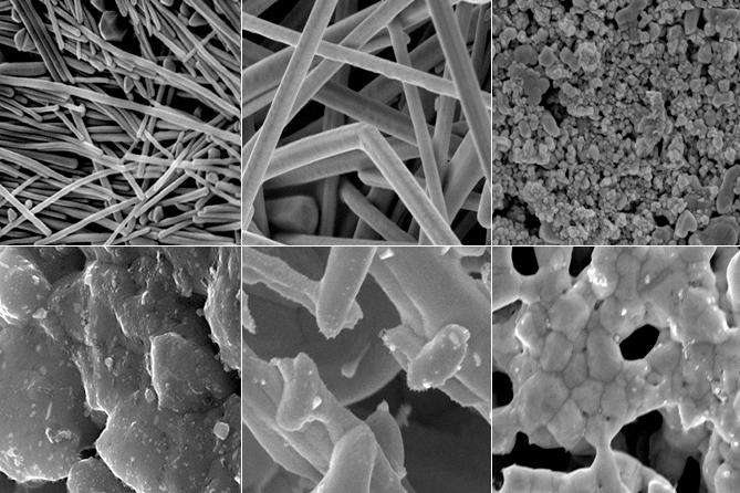
By comparing the conductivity of films made from different shapes of silver nanostructures, the researchers found that electrons zip through films made of silver nanowires much easier than films made from other shapes, like nanospheres or microflakes. In fact, electrons flowed so easily through the nanowire films that they could function in printed circuits without the need to melt them all together.

“The nanowires had a 4,000 times higher conductivity than the more commonly used silver nanoparticles that you would find in printed antennas for RFID tags,” said Benjamin Wiley, assistant professor of chemistry at Duke. “So if you use nanowires, then you don’t have to heat the printed circuits up to such high temperature and you can use cheaper plastics or paper.”

“There is really nothing else I can think of besides these silver nanowires that you can just print and it’s simply conductive, without any post-processing,” Wiley added.

These types of printed electronics could have applications far beyond smart packaging; researchers envision using the technology to make solar cells, printed displays, LEDS, touchscreens, amplifiers, batteries and even some implantable bio-electronic devices. The results appeared online Dec. 16 [2016] in ACS Applied Materials and Interfaces.

Silver has become a go-to material for making printed electronics, Wiley said, and a number of studies have recently appeared measuring the conductivity of films with different shapes of silver nanostructures. However, experimental variations make direct comparisons between the shapes difficult, and few reports have linked the conductivity of the films to the total mass of silver used, an important factor when working with a costly material.

“We wanted to eliminate any extra materials from the inks and simply hone in on the amount of silver in the films and the contacts between the nanostructures as the only source of variability,” said Ian Stewart, a recent graduate student in Wiley’s lab and first author on the ACS paper.

Stewart used known recipes to cook up silver nanostructures with different shapes, including nanoparticles, microflakes, and short and long nanowires, and mixed these nanostructures with distilled water to make simple “inks.” He then invented a quick and easy way to make thin films using equipment available in just about any lab — glass slides and double-sided tape.

“We used a hole punch to cut out wells from double-sided tape and stuck these to glass slides,” Stewart said. By adding a precise volume of ink into each tape “well” and then heating the wells — either to relatively low temperature to simply evaporate the water or to higher temperatures to begin melting the structures together — he created a variety of films to test.

The team say they weren’t surprised that the long nanowire films had the highest conductivity. Electrons usually flow easily through individual nanostructures but get stuck when they have to jump from one structure to the next, Wiley explained, and long nanowires greatly reduce the number of times the electrons have to make this “jump”.

But they were surprised at just how drastic the change was. “The resistivity of the long silver nanowire films is several orders of magnitude lower than silver nanoparticles and only 10 times greater than pure silver,” Stewart said.

The team is now experimenting with using aerosol jets to print silver nanowire inks in usable circuits. Wiley says they also want to explore whether silver-coated copper nanowires, which are significantly cheaper to produce than pure silver nanowires, will give the same effect.

Here’s a link to and a citation for the paper,

Effect of Morphology on the Electrical Resistivity of Silver Nanostructure Films by Ian E. Stewart, Myung Jun Kim, and Benjamin J. Wiley. ACS Appl. Mater. Interfaces, Article ASAP
DOI: 10.1021/acsami.6b12289 Publication Date (Web): December 16, 2016

Copyright © 2016 American Chemical Society

This paper is behind a paywall but there is an image of the silver nanowires, which is not exactly compensation but is interesting,

Caption: Duke University chemists have found that silver nanowire films like these conduct electricity well enough to form functioning circuits without applying high temperatures, enabling printable electronics on heat-sensitive materials like paper or plastic.
Credit: Ian Stewart and Benjamin Wiley

Generating clean fuel with individual gold atoms

A July 22, 2016 news item on Nanowerk highlights an international collaboration focused on producing clean fuel,

A combined experimental and theoretical study comprising researchers from the Chemistry Department and LCN [London Centre for Nanotechnology], along with groups in Argentina, China, Spain and Germany, has shed new light on the behaviour of individual gold atoms supported on defective thin cerium dioxide films – an important system for catalysis and the generation of clean hydrogen for fuel.

A July ??, 2016 LCN press release, which originated the news item, expands on the theme of catalysts, the research into individual gold atoms, and how all this could result in clean fuel,

Catalysis plays a vital role in our world; an estimated 80% of all chemical and materials are made via processes which involve catalysts, which are commonly a mixture of metals and oxides. The standard motif for these heterogeneous catalysts (where the catalysts are solid and the reactants are in the gas phase) is of a high surface area oxide support that is decorated with metal nanoparticles a few nanometres in diameter. Cerium dioxide (ceria, CeO2) is a widely used support material for many important industrial processes; metal nanoparticles supported on ceria have displayed high activities for applications including car catalytic converters, alcohol synthesis, and for hydrogen production. There are two key attributes of ceria which make it an excellent active support material: its oxygen storage and release ability, and its ability to stabilise small metal particles under reaction conditions. A recent system that has been the focus of much interest has been that of gold nanoparticles and single atoms with ceria, which has demonstrated high activity towards the water-gas-shift reaction, (CO + H2O —> CO2 + H2) a key stage in the generation of clean hydrogen for use in fuel cells.

The nature of the active sites of these catalysts and the role that defects play are still relatively poorly understood; in order to study them in a systematic fashion, the researchers prepared model systems which can be characterised on the atomic scale with a scanning tunnelling microscope.

Figure: STM images of CeO2-x(111) ultrathin films before and after the deposition of Au single atoms at 300 K. The bright lattice is from the oxygen atoms at the surface – vacancies appear as dark spots

These model systems comprised well-ordered, epitaxial ceria films less than 2 nm thick, prepared on a metal single crystal, upon which single atoms and small clusters of gold were evaporated onto under ultra-high-vacuum (essential to prevent contamination of the surfaces). Oxygen vacancy defects – missing oxygen atoms in the top layer of the ceria – are relatively common at the surface and appear as dark spots in the STM images. By mapping the surface before and after the deposition of gold, it is possible to analyse the binding of the metal atoms, in particular there does not appear to be any preference for binding in the vacancy sites at 300 K.

Publishing their results in Physical Review Letters, the researchers combined these experimental results with theoretical studies of the binding energies and diffusion rates across the surface. They showed that kinetic effects governed the behaviour of the gold atoms, prohibiting the expected occupation of the thermodynamically more stable oxygen vacancy sites. They also identified electron transfer between the gold atoms and the ceria, leading to a better understanding of the diffusion phenomena that occur at this scale, and demonstrated that the effect of individual surface defects may be more minor than is normally imagined.

Here’s a link to and a citation for the paper,

Diffusion Barriers Block Defect Occupation on Reduced CeO2(111) by P.G. Lustemberg, Y. Pan, B.-J. Shaw, D. Grinter, Chi Pang, G. Thornton, Rubén Pérez, M. V. Ganduglia-Pirovano, and N. Nilius. Phys. Rev. Lett. Vol. 116, Iss. 23 — 10 June 2016 2016DOI:http://dx.doi.org/10.1103/PhysRevLett.116.236101 Published 9 June 2016

This paper is behind a paywall.

Nanowalls (like waffles) for touchscreens

ETH Zurich has announced a new technique for creating transparent electrodes in a Jan. 6, 2016 news item on ScienceDaily,

Transparent electrodes have been manufactured for use in touchscreens using a novel nanoprinting process. The new electrodes are some of the most transparent and conductive that have ever been developed.

From smartphones to the operating interfaces of ticket machines and cash dispensers, every touchscreen we use requires transparent electrodes: The devices’ glass surface is coated with a barely visible pattern made of conductive material. It is because of this that the devices recognise whether and where exactly a finger is touching the surface.

Here’s an image illustrating the new electrodes,

With a special mode of electrohydrodynamic ink-jet printing scientists can create a grid of ultra fine gold walls. (Visualisations: Ben Newton / Digit Works)

With a special mode of electrohydrodynamic ink-jet printing scientists can create a grid of ultra fine gold walls. (Visualisations: Ben Newton / Digit Works)

I think these electrodes resemble waffles,

[downloaded from https://github.com/jhermann/Stack-O-Waffles] Credit: jherman

[downloaded from https://github.com/jhermann/Stack-O-Waffles] Credit: jherman

Getting back to the electrodes themselves, a Jan. 6, 2016 ETH Zurich press release (also on EurekAlert*)by Fabio Bergamin, which originated the news item, provides more details,

Researchers under the direction of Dimos Poulikakos, Professor of Thermodynamics, have now used 3D print technology to create a new type of transparent electrode, which takes the form of a grid made of gold or silver “nanowalls” on a glass surface. The walls are so thin that they can hardly be seen with the naked eye. It is the first time that scientists have created nanowalls like these using 3D printing. The new electrodes have a higher conductivity and are more transparent than those made of indium tin oxide, the standard material used in smartphones and tablets today. This is a clear advantage: The more transparent the electrodes, the better the screen quality. And the more conductive they are, the more quickly and precisely the touchscreen will work.

Third dimension

“Indium tin oxide is used because the material has a relatively high degree of transparency and the production of thin layers has been well researched, but it is only moderately conductive,” says Patrik Rohner, a PhD student in Poulikakos’ team. In order to produce more conductive electrodes, the ETH researchers opted for gold and silver, which conduct electricity much better. But because these metals are not transparent, the scientists had to make use of the third dimension. ETH professor Poulikakos explains: “If you want to achieve both high conductivity and transparency in wires made from these metals, you have a conflict of objectives. As the cross-sectional area of gold and silver wires grows, the conductivity increases, but the grid’s transparency decreases.”

The solution was to use metal walls only 80 to 500 nanometres thick, which are almost invisible when viewed from above. Because they are two to four times taller than they are wide, the cross-sectional area, and thus the conductivity, is sufficiently high.

Ink-jet printer with tiny print head

The researchers produced these tiny metal walls using a printing process known as Nanodrip, which Poulikakos and his colleagues developed three years ago. Its basic principle is a process called electrohydrodynamic ink-jet printing. In this process scientists use inks made from metal nanoparticles in a solvent; an electrical field draws ultra-small droplets of the metallic ink out of a glass capillary. The solvent evaporates quickly, allowing a three-dimensional structure to be built up drop by drop.

What is special about the Nanodrip process is that the droplets that come out of the glass capillary are about ten times smaller than the aperture itself. This allows for much smaller structures to be printed. “Imagine a water drop hanging from a tap that is turned off. And now imagine that another tiny droplet is hanging from this drop – we are only printing the tiny droplet,” Poulikakos explains. The researchers managed to create this special form of droplet by perfectly balancing the composition of metallic ink and the electromagnetic field used.

Cost-efficient production

The next big challenge will now be to upscale the method and develop the print process further so that it can be implemented on an industrial scale. To achieve this, the scientists are working with colleagues from ETH spin-off company Scrona.

Here’s a link to and a citation for the paper,

Electrohydrodynamic NanoDrip Printing of High Aspect Ratio Metal Grid Transparent Electrodes by Julian Schneider, Patrick Rohner, Deepankur Thureja, Martin Schmid, Patrick Galliker, Dimos Poulikalos. Advanced Functional Materials DOI: 10.1002/adfm.201503705 First published: 15 December 2015

This paper is behind a paywall.

*'(also on EurekAlert)’ added on Jan. 7, 2016.