Tag Archives: microscopy

Nanotech business news from Turkey and from Northern Ireland

I have two nanotech business news bits, one from Turkey and one from Northern Ireland.

Turkey

A Turkish company has sold one of its microscopes to the US National Aeronautics and Space Administration (NASA), according to a Jan. 20, 2017 news item on dailysabah.com,

Turkish nanotechnology company Nanomanyetik has begun selling a powerful microscope to the U.S. space agency NASA, the company’s general director told Anadolu Agency on Thursday [Jan. 19, 2017].

Dr. Ahmet Oral, who also teaches physics at Middle East Technical University, said Nanomanyetik developed a microscope that is able to map surfaces on the nanometric and atomic levels, or extremely small particles.

Nanomanyetik’s foreign customers are drawn to the microscope because of its higher quality yet cheaper price compared to its competitors.

“There are almost 30 firms doing this work,” according to Oral. “Ten of them are active and we are among these active firms. Our aim is to be in the top three,” he said, adding that Nanomanyetik jumps to the head of the line because of its after-sell service.

In addition to sales to NASA, the Ankara-based firm exports the microscope to Brazil, Chile, France, Iran, Israel, Italy, Japan, Poland, South Korea and Spain.

Electronics giant Samsung is also a customer.

“Where does Samsung use this product? There are pixels in the smartphones’ displays. These pixels are getting smaller each year. Now the smallest pixel is 15X10 microns,” he said. Human hair is between 10 and 100 microns in diameter.

“They are figuring inner sides of pixels so that these pixels can operate much better. These patterns are on the nanometer level. They are using these microscopes to see the results of their works,” Oral said.

Nanomanyetik’s microscopes produces good quality, high resolution images and can even display an object’s atoms and individual DNA fibers, according to Oral.

You can find the English language version of the Nanomanyetik (NanoMagnetics Instruments) website here . For those with the language skills there is the Turkish language version, here.

Northern Ireland

A Jan. 22, 2017 news article by Dominic Coyle for The Irish Times (Note: Links have been removed) shares this business news and mention of a world first,

MOF Technologies has raised £1.5 million (€1.73 million) from London-based venture capital group Excelsa Ventures and Queen’s University Belfast’s Qubis research commercialisation group.

MOF Technologies chief executive Paschal McCloskey welcomed the Excelsa investment.

Established in part by Qubis in 2012 in partnership with inventor Prof Stuart James, MOF Technologies began life in a lab at the School of Chemistry and Chemical Engineering at Queen’s.

Its metal organic framework (MOF) technology is seen as having significant potential in areas including gas storage, carbon capture, transport, drug delivery and heat transformation. Though still in its infancy, the market is forecast to grow to £2.2 billion by 2022, the company says.

MOF Technologies last year became the first company worldwide to successfully commercialise MOFs when it agreed a deal with US fruit and vegetable storage provider Decco Worldwide to commercialise MOFs for use in a food application.

TruPick, designed by Decco and using MOF Technologies’ environmentally friendly technology, enables nanomaterials control the effects of ethylene on fruit produce so it maintains freshness in storage or transport.

MOFs are crystalline, sponge-like materials composed of two components – metal ions and organic molecules known as linkers.

“We very quickly recognised the market potential of MOFs in terms of their unmatched ability for gas storage,” said Moritz Bolle from Excelsa Ventures. “This technology will revolutionise traditional applications and open countless new opportunities for industry. We are confident MOF Technologies is the company that will lead this seismic shift in materials science.

You can find MOF Technologies here.

Functional hybrid system that can connect human tissue with electronic devices

I’ve tagged this particular field of interest ‘machine/flesh’ because I find it more descriptive than ‘bio-hybrid system’ which was the term used in a Nov. 15, 2016 news item on phys.org,

One of the biggest challenges in cognitive or rehabilitation neurosciences is the ability to design a functional hybrid system that can connect and exchange information between biological systems, like neurons in the brain, and human-made electronic devices. A large multidisciplinary effort of researchers in Italy brought together physicists, chemists, biochemists, engineers, molecular biologists and physiologists to analyze the biocompatibility of the substrate used to connect these biological and human-made components, and investigate the functionality of the adhering cells, creating a living biohybrid system.

A Nov.15, 2016 American Institute of Physics news release on EurekAlert, which originated the news item, details the investigation,

In an article appearing this week in AIP Advances, from AIP Publishing, the research team used the interaction between light and matter to investigate the material properties at the molecular level using Raman spectroscopy, a technique that, until now, has been principally applied to material science. Thanks to the coupling of the Raman spectrometer with a microscope, spectroscopy becomes a useful tool for investigating micro-objects such as cells and tissues. Raman spectroscopy presents clear advantages for this type of investigation: The molecular composition and the modi?cation of subcellular compartments can be obtained in label-free conditions with non-invasive methods and under physiological conditions, allowing the investigation of a large variety of biological processes both in vitro and in vivo.

Once the biocompatibility of the substrate was analyzed and the functionality of the adhering cells investigated, the next part of this puzzle is connecting with the electronic component. In this case a memristor was used.

“Its name reveals its peculiarity (MEMory ResISTOR), it has a sort of “memory”: depending on the amount of voltage that has been applied to it in the past, it is able to vary its resistance, because of a change of its microscopic physical properties,” said Silvia Caponi, a physicist at the Italian National Research Council in Rome. By combining memristors, it is possible to create pathways within the electrical circuits that work similar to the natural synapses, which develop variable weight in their connections to reproduce the adaptive/learning mechanism. Layers of organic polymers, like polyaniline (PANI) a semiconductor polymer, also have memristive properties, allowing them to work directly with biological materials into a hybrid bio-electronic system.

“We applied the analysis on a hybrid bio-inspired device but in a prospective view, this work provides the proof of concept of an integrated study able to analyse the status of living cells in a large variety of applications that merges nanosciences, neurosciences and bioelectronics,” said Caponi. A natural long-term objective of this work would be interfacing machines and nervous systems as seamlessly as possible.

The multidisciplinary team is ready to build on this proof of principle to realize the potential of memristor networks.

“Once assured the biocompatibility of the materials on which neurons grow,” said Caponi, “we want to define the materials and their functionalization procedures to find the best configuration for the neuron-memristor interface to deliver a full working hybrid bio-memristive system.”

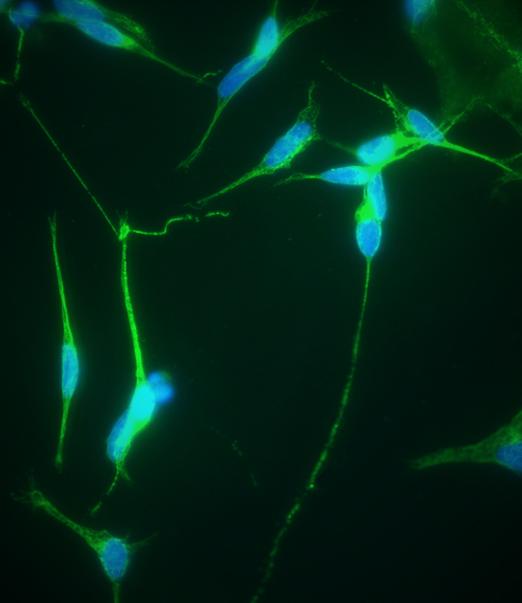
Caption: These are immunofluorescence analysis of SH-SY5Y cells treated for 5 days with 10uM Retinoic Acid and 50ng/ml BDNF for the next 3 days. The DAPI fluorescence stain is blue and Beta-tubulin is green. Credit: Caponi, et al.

Caption: These are immunofluorescence analysis of SH-SY5Y cells treated for 5 days with 10uM Retinoic Acid and 50ng/ml BDNF for the next 3 days. The DAPI fluorescence stain is blue and Beta-tubulin is green. Credit: Caponi, et al.

Here’s a link to and a citation for the paper,

A multidisciplinary approach to study the functional properties of neuron-like cell models constituting a living bio-hybrid system: SH-SY5Y cells adhering to PANI substrate by S. Caponi, S. Mattana, M. Ricci, K. Sagini, L. J. Juarez-Hernandez, A. M. Jimenez-Garduño, N. Cornella, L. Pasquardini, L. Urbanelli, P. Sassi, A. Morresi, C. Emiliani, D. Fioretto, M. Dalla Serra, C. Pederzolli, S. Iannotta, P. Macchi, and C. Musio. AIP Advances 6, 111303 (2016); http://dx.doi.org/10.1063/1.4966587

This paper appears to be open access.

Atomic force microscope with nanowire sensors

Measuring the size and direction of forces may become reality with a nanotechnology-enabled atomic force microscope designed by Swiss scientists, according to an Oct. 17, 2016 news item on phys.org,

A new type of atomic force microscope (AFM) uses nanowires as tiny sensors. Unlike standard AFM, the device with a nanowire sensor enables measurements of both the size and direction of forces. Physicists at the University of Basel and at the EPF Lausanne have described these results in the recent issue of Nature Nanotechnology.

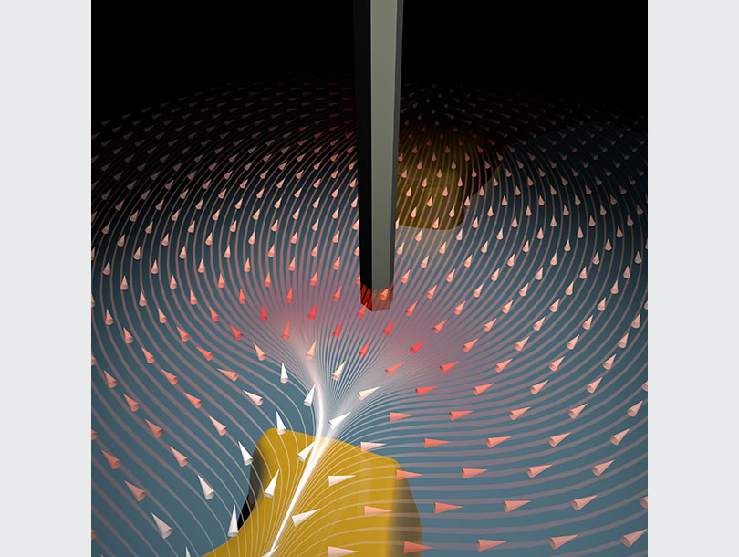
A nanowire sensor measures size and direction of forces (Image: University of Basel, Department of Physics)

A nanowire sensor measures size and direction of forces (Image: University of Basel, Department of Physics)

An Oct. 17, 2016 University of Basel press release (also on EurekAlert), which originated the news item, expands on the theme,

Nanowires are extremely tiny filamentary crystals which are built-up molecule by molecule from various materials and which are now being very actively studied by scientists all around the world because of their exceptional properties.

The wires normally have a diameter of 100 nanometers and therefore possess only about one thousandth of a hair thickness. Because of this tiny dimension, they have a very large surface in comparison to their volume. This fact, their small mass and flawless crystal lattice make them very attractive in a variety of nanometer-scale sensing applications, including as sensors of biological and chemical samples, and as pressure or charge sensors.

Measurement of direction and size

The team of Argovia Professor Martino Poggio from the Swiss Nanoscience Institute (SNI) and the Department of Physics at the University of Basel has now demonstrated that nanowires can also be used as force sensors in atomic force microscopes. Based on their special mechanical properties, nanowires vibrate along two perpendicular axes at nearly the same frequency. When they are integrated into an AFM, the researchers can measure changes in the perpendicular vibrations caused by different forces. Essentially, they use the nanowires like tiny mechanical compasses that point out both the direction and size of the surrounding forces.

Image of the two-dimensional force field

The scientists from Basel describe how they imaged a patterned sample surface using a nanowire sensor. Together with colleagues from the EPF Lausanne, who grew the nanowires, they mapped the two-dimensional force field above the sample surface using their nanowire “compass”. As a proof-of-principle, they also mapped out test force fields produced by tiny electrodes.

The most challenging technical aspect of the experiments was the realization of an apparatus that could simultaneously scan a nanowire above a surface and monitor its vibration along two perpendicular directions. With their study, the scientists have demonstrated a new type of AFM that could extend the technique’s numerous applications even further.

AFM – today widely used

The development of AFM 30 years ago was honored with the conferment of the Kavli-Prize [2016 Kavli Prize in Nanoscience] beginning of September this year. Professor Christoph Gerber of the SNI and Department of Physics at the University of Basel is one of the awardees, who has substantially contributed to the wide use of AFM in different fields, including solid-state physics, materials science, biology, and medicine.

The various different types of AFM are most often carried out using cantilevers made from crystalline Si as the mechanical sensor. “Moving to much smaller nanowire sensors may now allow for even further improvements on an already amazingly successful technique”, Martino Poggio comments his approach.

I featured an interview article with Christoph Gerber and Gerd Binnig about their shared Kavli prize and about inventing the AFM in a Sept. 20, 2016 posting.

As for the latest innovation, here’s a link to and a citation for the paper,

Vectorial scanning force microscopy using a nanowire sensor by Nicola Rossi, Floris R. Braakman, Davide Cadeddu, Denis Vasyukov, Gözde Tütüncüoglu, Anna Fontcuberta i Morral, & Martino Poggio. Nature Nanotechnology (2016) doi:10.1038/nnano.2016.189 Published online 17 October 2016

This paper is behind a paywall.

All about Atomic Force Microscopy (AFM) with Gerd Binnig and Christoph Gerber

Gerd Binnig, Christoph Gerber, and Calvin Quate invented the atomic force microscope in the 1980s and an Aug. 16, 2016 news item on Nanotechnology Now announces a discussion with two of the inventors, Binnig and Gerber (Note: Links have been removed),

The inventors of one of the most versatile tools in modern science – the atomic force microscope, or AFM – tell their story in an interview published online this week. The AFM was invented in the mid 1980s by Gerd Binnig, Christoph Gerber and Calvin Quate, three physicists who are sharing the 2016 Kavli Prize in Nanoscience.

Binnig and Gerber discuss their inspiration for the device, how they solved problems through sport, and why their invention continues to propel science at the nanoscale.

This charming Aug. 20, 2016 discussion for the Kavli Foundation focuses on more than the AFM although it is the main topic,

Our roundtable panelists were:

GERD BINNIG –is a physicist and Nobel Laureate for his invention (with Heinrich Rohrer and Christoph Gerber) of the scanning tunneling microscope while at IBM Zurich. He began development of the atomic force microscope in 1986 to overcome the limitations of his previous invention.
CHRISTOPH GERBER –is a physicist and director for scientific communication at the Swiss Nanoscience Institute at the University of Basel. While at IBM, Gerber worked closely with Binnig on bringing both the scanning tunneling microscope and atomic force microscope to fruition.

Calvin Quate was unable to participate in the roundtable. The transcript has been amended and edited by the laureates

THE KAVLI FOUNDATION [TKF]: You filed your first patent for the atomic force microscope (AFM) nearly 30 years ago. How has it changed the way we look at the world since then?

GERD BINNIG: It was like the first time people looked through an optical microscope and saw bacteria. That completely changed how we look at the world. Suddenly, we understood what was really going on in nature, and we used that knowledge to learn how diseases spread. The AFM is the next step. It lets us look at the molecules that make life possible in those bacteria – and everywhere else – and see things we could not see before. It teaches us how to make changes to surfaces or molecules that we attempted blindly in the past. And it has been used in so many different scientific studies, from looking at polymers and chemical reactions to modifying surfaces at the atomic level.

CHRISTOPH GERBER: As Gerd explained, seeing is believing, and now we can do that onthe atomic scale. AFM has turned into the most powerful and most versatile toolkit that we have for doing nanoscience. And it keeps evolving. In just the past few years, researchers have learned to pick up a molecule on the tip of an AFM, which we can think of as the needle on a record player, and reveal chemical bonds while imaging molecules on surfaces. Nobody thought that ever would be possible.

TKF: Has this changed how researchers think about the ways nanoscale interactions affect the things they study?

BINNIG: Very much so. Before AFM, people who wanted to model very small structures –molecules, cell walls, semiconductors – had to make indirect measurements of them. But those structures can be complex and disordered, and indirect measurements do not always capture that, so the models they came up with were often wrong. But now, we can look at those structures and adapt our models to match what we observe. We as scientists always have to connect our theories to reality. Atomic force microscopy lets us do this.

TKF: When you started thinking about the AFM, biology was one of the fields you had inmind. Yet even you must have been surprised at how it has revolutionized biology.

GERBER: Yes. AFM’s capabilities keep evolving, and researchers are always finding new ways to use it. For example, in recent years, researchers have made tremendous progress in taking AFM measurements in real time. It’s like watching a movie. They can now see biological interactions, such as how molecules degrade or how antimicrobials attack bacterial membranes as they occur – something nobody could have foreseen 20 years ago. It took 15 years to get there, but we can now see biology in action and compare that to our theories.

BINNIG: Exactly. In biology, the biggest and most important question is always whether a molecule will bind to another molecule, change it, and by changing it cause something important to happen. This is all about forces, and researchers can use AFM to bring two molecules or even two cells close together, or pull them apart, and measure those forces directly. We can learn how big those forces are and under what conditions they occur. We’re actually looking into the heart of biology when we do that.

GERBER: And atomic force microscopy can tell us about many different types of forces that determine the outcome of chemical reactions at the nanoscale. These range from chemical, mechanical and electrostatic through, most recently, to the very weak interactions between molecules.

BINNIG: A great example of this is how Hermann Gaub, a professor of biophysics at Ludwig Maximilians University of Munich, used AFM to unfold proteins. He actually attached one end of a protein to a surface and the other end to an AFM tip. When he pulled the tip up, the protein straightened out and he could create a fingerprint of the unfolding forces that he could compare with his model.

TKF: What about applications you could not have foreseen?

BINNIG: I could not have foreseen that we can image molecules with such a high resolution. It’s unbelievable. We can see the bonds between molecules. We can watch them change during a chemical reaction, and sometimes there are surprises. Some researchers have observed an intermediate state in a chemical reaction that should not have lasted long enough to see. So they have had to rethink their theories to take into account why this intermediate state lasted so long. That’s what happens when we can observe such high-resolution details.

GERBER: Another example is high-speed AFM, which biologists use to see the cellular machinery in action. No other technique can do that. It works by tapping a very, very thin cantilever up and down, taking one quick measurement after another.

BINNIG: It is amazing how many people use the AFM in so many different fields. We first thought, well, maybe biology or semiconductor research. But it was picked up everywhere, from studying friction to cosmetics.

GERBER: I recently looked it up, and AFM was mentioned in 353,000 peer-reviewed papers. Our original article was published in Physical Review Letters, the top journal in the field in which all the important theoretical work is published. Ours is the only experimental paper on its list of most-cited papers.

TKF: Amazing. And yet AFM was actually a follow-up to another technology you worked on, the scanning tunneling microscope, or STM. It was probably the first instrument to achieve nanoscale resolution without using electrons or other high-energy beams that can damage what you are observing, right?

BINNIG: Yes.

TKF: And where did that idea come from?

BINNIG: We were trying to solve a problem. IBM was working on a new type of semiconductor chip, and the insulator, which keeps the electric current from escaping the semiconductor, was leaking. But no one knew why. So Heinrich Rohrer, who was working at IBM Zurich, hired me. I looked to all the available instruments, and none of them could study materials on such a fine scale to find out.

So the two of us thought, well, okay, we’ll invent something. We thought we could take advantage of something called quantum tunneling. Quantum tunneling is when an electron tunnels through a conducting material and come out the other side. We developed STM to map the surface of the material by measuring where electrons emerged on the other side. Only later did we realize that we could move our probe from one spot to cover the entire surface.

TKF: Dr. Gerber, you quickly became part of the STM team. What convinced you to join?

GERBER: I felt this was such a crazy idea, and I’m always very fond of this sort of thing. I thought this was fantastic.

BINNIG: I can confirm this. Christoph always likes crazy things. That runs through his life.

GERBER: Actually, the development of STM was kind of an undercover project at the beginning, because Gerd and Heinrich were involved in other projects. I worked for a year or so on my own. When we started overcoming problems and we could see features on the surface of a material that were one-tenth of a nanometer, then it really took off.
I leave you to discover the discussion in its entirety: Aug. 20, 2016 discussion.

Spider silk as a bio super-lens

Bangor University (Wales, UK) is making quite the impact these days. I’d never heard of the institution until their breakthrough with nanobeads (Sept. 7, 2016 posting) to break through a resolution barrier and now there’s a second breakthrough with their partners at Oxford University (England, UK). From an Aug. 19, 2016 news item on ScienceDaily (Note: A link has been removed),

Scientists at the UK’s Bangor and Oxford universities have achieved a world first: using spider-silk as a superlens to increase the microscope’s potential.

Extending the limit of classical microscope’s resolution has been the ‘El Dorado’ or ‘Holy Grail’ of microscopy for over a century. Physical laws of light make it impossible to view objects smaller than 200 nm — the smallest size of bacteria, using a normal microscope alone. However, superlenses which enable us to see beyond the current magnification have been the goal since the turn of the millennium.

Hot on the heels of a paper (Sci. Adv. 2 e1600901,2016) revealing that a team at Bangor University’s School of Electronic Engineering has used a nanobead-derived superlens to break the perceived resolution barrier, the same team has achieved another world first.

Now the team, led by Dr Zengbo Wang and in colloboration with Prof. Fritz Vollrath’s silk group at Oxford University’s Department of Zoology, has used a naturally occurring material — dragline silk of the golden web spider, as an additional superlens, applied to the surface of the material to be viewed, to provide an additional 2-3 times magnification.

This is the first time that a naturally occurring biological material has been used as a superlens.

An Aug. 19, 2016 Bangor University press release (also on EurekAlert), which originated the news item, provides more information about the new work,

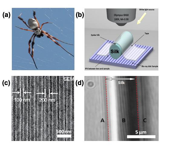
In the paper in Nano Letters (DOI: 10.1021/acs.nanolett.6b02641, Aug 17 2016), the joint team reveals how they used a cylindrical piece of spider silk from the thumb sized Nephila spider as a lens.

Dr Zengbo Wang said:

“We have proved that the resolution barrier of microscope can be broken using a superlens, but production of manufactured superlenses invovles some complex engineering processes which are not widely accessible to other reserchers. This is why we have been interested in looking for naturally occurring superlenses provided by ‘Mother Nature’, which may exist around us, so that everyone can access superlenses.”

Prof Fritz Vollrath adds:

“It is very exciting to find yet another cutting edge and totally novel use for a spider silk, which we have been studying for over two decades in my laboratory.”

These lenses could be used for seeing and viewing previously ‘invisible’ structures, including engineered nano-structures and biological micro-structures as well as, potentially, native germs and viruses.

The natural cylindrical structure at a micron- and submicron-scale make silks ideal candidates, in this case, the individual filaments had diameters of one tenth of a thin human hair.

The spider filament enabled the group to view details on a micro-chip and a blue- ray disk which would be invisible using the unmodified optical microscope.

In much the same was as when you look through a cylindrical glass or bottle, the clearest image only runs along the narrow strip directly opposite your line of vision, or resting on the surface being viewed, the single filament provides a one dimensional viewing image along its length.

Wang explains:

“The cylindrical silk lens has advantages in the larger field-of-view when compared to a microsphere superlens. Importantly for potential commercial applications, a spider silk nanoscope would be robust and economical, which in turn could provide excellent manufacturing platforms for a wide range of applications.”

James Monks, a co-author on the paper comments: “it has been an exciting time to be able to develop this project as part of my honours degree in electronic engineering at Bangor University and I am now very much looking forward to joining Dr Wang’s team as a PhD student in nano-photonics.”

The researchers have provided a close up image with details,

Caption: (a) Nephila edulis spider in its web. (b) Schematic drawing of reflection mode silk biosuperlens imaging. The spider silk was placed directly on top of the sample surface by using a soft tape, which magnify underlying nano objects 2-3 times (c) SEM image of Blu-ray disk with 200/100 nm groove and lines (d) Clear magnified image (2.1x) of Blu-ray disk under spider silk superlens. Credit: Bangor University/ University of Oxford

Caption: (a) Nephila edulis spider in its web. (b) Schematic drawing of reflection mode silk biosuperlens imaging. The spider silk was placed directly on top of the sample surface by using a soft tape, which magnify underlying nano objects 2-3 times (c) SEM image of Blu-ray disk with 200/100 nm groove and lines (d) Clear magnified image (2.1x) of Blu-ray disk under spider silk superlens. Credit: Bangor University/ University of Oxford

Here’s a link to and a citation for the ‘spider silk’ superlens paper,

Spider Silk: Mother Nature’s Bio-Superlens by James N. Monks, Bing Yan, Nicholas Hawkins, Fritz Vollrath, and Zengbo Wang. Nano Lett., Article ASAP DOI: 10.1021/acs.nanolett.6b02641 Publication Date (Web): August 17, 2016

Copyright © 2016 American Chemical Society

This paper is behind a paywall.

A new lens (made from nanobeads) for seeing subwavelength images at visible frequencies

The image which illustrates the research is quite intriguing but I don’t think it makes much sense until you read about the research. From an Aug. 12, 2016 news item on ScienceDaily,

Nanobeads are all around us- and are, some might argue, used too frequently in everything from sun-screen to white paint, but a new ground-breaking application is revealing hidden worlds.

A paper in Science Advances provides proof of a new concept, using new solid 3D superlenses to break through the scale of things previously visible through a microscope.

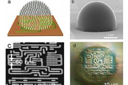
Illustrating the strength of the new superlens, the scientists describe seeing for the first time, the actual information on the surface of a Blue Ray DVD. That shiny surface is not as smooth as we think. Current microscopes cannot see the grooves containing the data- but now even the data itself is revealed.

Now the image,

(a) Conceptual drawing of nanoparticle-based metamaterial solid immersion lens (mSIL) (b) Lab made mSIL (c) SEM image of 60 nm sized imaging sample (d) corresponding superlens imaging of the 60 nm samples by the developed mSIL. Courtesy: Bangor University

(a) Conceptual drawing of nanoparticle-based metamaterial solid immersion lens (mSIL) (b) Lab made mSIL (c) SEM image of 60 nm sized imaging sample (d) corresponding superlens imaging of the 60 nm samples by the developed mSIL. Credit: ©BangorUniversity Fudan University

An Aug. 13, 2016 Bangor University press release (also on EurekAlert with an Aug. 12, 2016 publication date), which originated the news item, describes the work in more detail,

Led by Dr Zengbo Wang at Bangor University UK and Prof Limin Wu at Fudan University, China, the team created minute droplet-like lens structures on the surface to be examined. These act as an additional lens to magnify the surface features previously invisible to a normal lens.

Made of millions of nanobeads, the spheres break up the light beam. Each bead refracts the light, acting as individual torch-like minute beam. It is the very small size of each beam of light which illuminate the surface, extending the resolving ability of the microscope to record-breaking levels. The new superlens adds 5x magnification on top of existing microscopes.

Extending the limit of classical microscope’s resolution has been the ‘El Dorado’ or ‘Holy Grail’ of microscopy for over a century. Physical laws of light make it impossible to view objects smaller than 200 nm – the smallest size of bacteria, using a normal microscope alone. However, superlenses have been the new goal since the turn of the millennium, with various labs and teams researching different models and materials.

“We’ve used high-index titanium dioxide (TiO2) nanoparticles as the building element of the lens. These nanoparticles are able to bend light to a higher degree than water. To explain, when putting a spoon into a cup of this material, if it were possible, you’d see a larger bend where you spoon enters the material than you would looking at the same spoon in a glass of water,” Dr Wang says.

Nanoparticles splitting single incident beam into multiple=Nanoparticles splitting single incident beam into multiple beams which provides optical super-resolution in imaging.“Each sphere bends the light to a high magnitude and splits the light beam, creating millions of individual beams of light. It is these tiny light beams which enable us to view previously unseen detail.”

Wang believes that the results will be easily replicable and that other labs will soon be adopting the technology and using it for themselves.

The advantages of the technology is that the material, titanium dioxide, is cheap and readily available, and rather than buying a new microscope, the lenses are applied to the material to be viewed, rather than to the microscope.

“We have already viewed details to a far greater level than was previously possible. The next challenge is to adapt the technology for use in biology and medicine. This would not require the current use of a combination of dyes and stains and laser light- which change the samples being viewed. The new lens will be used to see germs and viruses not previously visible.”

Here’s a link to and a citation for the paper,

Three-dimensional all-dielectric metamaterial solid immersion lens for subwavelength imaging at visible frequencies by Wen Fan, Bing Yan, Zengbo Wang, and Limin Wu. Science Advances  12 Aug 2016: Vol. 2, no. 8, e1600901 DOI: 10.1126/sciadv.1600901

This paper is open access.

Nuclear magnetic resonance microscope breaks records

Dutch researchers have found a way to apply the principles underlying magnetic resonance imaging (MRI) to a microscope designed *for* examining matter and life at the nanoscale. From a July 15, 2016 news item on phys.org,

A new nuclear magnetic resonance (NMR) microscope gives researchers an improved instrument to study fundamental physical processes. It also offers new possibilities for medical science—for example, to better study proteins in Alzheimer’s patients’ brains. …

A Leiden Institute of Physics press release, which originated the news item, expands on the theme,

If you get a knee injury, physicians use an MRI machine to look right through the skin and see what exactly is the problem. For this trick, doctors make use of the fact that our body’s atomic nuclei are electrically charged and spin around their axis. Just like small electromagnets they induce their own magnetic field. By placing the knee in a uniform magnetic field, the nuclei line up with their axis pointing in the same direction. The MRI machine then sends a specific type of radio waves through the knee, causing some axes to flip. After turning off this signal, those nuclei flip back after some time, under excitation of a small radio wave. Those waves give away the atoms’ location, and provide physicians with an accurate image of the knee.

NMR

MRI is the medical application of Nuclear Magnetic Resonance (NMR), which is based on the same principle and was invented by physicists to conduct fundamental research on materials. One of the things they study with NMR is the so-called relaxation time. This is the time scale at which the nuclei flip back and it gives a lot of information about a material’s properties.

Microscope

To study materials on the smallest of scales as well, physicists go one step further and develop NMR microscopes, with which they study the mechanics behind physical processes at the level of a group of atoms. Now Leiden PhD students Jelmer Wagenaar and Arthur de Haan have built an NMR microscope, together with principal investigator Tjerk Oosterkamp, that operates at a record temperature of 42 milliKelvin—close to absolute zero. In their article in Physical Review Applied they prove it works by measuring the relaxation time of copper. They achieved a thousand times higher sensitivity than existing NMR microscopes—also a world record.

Alzheimer

With their microscope, they give physicists an instrument to conduct fundamental research on many physical phenomena, like systems displaying strange behavior in extreme cold. And like NMR eventually led to MRI machines in hospitals, NMR microscopes have great potential too. Wagenaar: ‘One example is that you might be able to use our technique to study Alzheimer patients’ brains at the molecular level, in order to find out how iron is locked up in proteins.’

Here’s a link to and a citation for the paper,

Probing the Nuclear Spin-Lattice Relaxation Time at the Nanoscale by J. J. T. Wagenaar, A. M. J. den Haan, J. M. de Voogd, L. Bossoni, T. A. de Jong, M. de Wit, K. M. Bastiaans, D. J. Thoen, A. Endo, T. M. Klapwijk, J. Zaanen, and T. H. Oosterkamp. Phys. Rev. Applied 6, 014007 DOI:http://dx.doi.org/10.1103/PhysRevApplied.6.014007 Published 15 July 2016

This paper is open access.

*’fro’ changed to ‘for’ on Aug. 3, 2016.

Making ordinary microscopes image objects at the nanoscale

The researchers believe this technique for making ordinary microscopes capable of nanoscale imaging will make research into diseases easier, especially in developing countries. A July 20, 2016 news item on phys.org announces the new technique,

Research completed through a collaboration with University of Missouri [MU] engineers, biologists, and chemists could transform how scientists study molecules and cells at sub-microscopic (nanoscale) levels. Shubra Gangopadhyay, an electrical and computer engineer and her team at MU recently published studies outlining a new, relatively inexpensive imaging platform that enables single molecule imaging. This patented method highlights Gangopadhyay’s more than 30 years of nanoscale research that has proven invaluable in biological research and battling diseases.

This diagram shows the difference between regular and plasmonic gratings in terms of fluorescent intensity. Credit: Shubhra Gangopadhyay/Nanoscale.

This diagram shows the difference between regular and plasmonic gratings in terms of fluorescent intensity. Credit: Shubhra Gangopadhyay/Nanoscale.

A July 19, 2016 University of Missouri news release (also received via email), which originated the news item, explains further,

“Usually, scientists have to use very expensive microscopes to image at the sub-microscopic level,” said Gangopadhyay, the C.W. LaPierre Endowed Chair of electrical and computer engineering in the MU College of Engineering. “The techniques we’ve established help to produce enhanced imaging results with ordinary microscopes. The relatively low production cost for the platform also means it could be used to detect a wide variety of diseases, particularly in developing countries.”

The team’s custom platform uses an interaction between light and the surface of the metal grating to generate surface plasmon resonance (SPR), a rapidly developing imaging technique that enables super-resolution imaging down to 65 nanometers—a resolution normally reserved for electron microscopes. Using HD-DVD and Blu-Ray discs as starting templates, a repeating grating pattern is transferred onto the microscope slides where the specimen will be placed. Since the patterns originate from a widely used technology, the manufacturing process remains relatively inexpensive.

“In previous studies, we’ve used plasmonic gratings to detect cortisol and even tuberculosis,” Gangopadhyay said. “Additionally, the relatively low production cost for the platform also means it could be used to further detect a wide variety of diseases, particularly in developing countries. Eventually, we might even be able to use smartphones to detect disease in the field.”

Here’s a link to and a citation for the paper,

Plasmonic gratings with nano-protrusions made by glancing angle deposition for single-molecule super-resolution imaging by B. Chen, A. Wood, A. Pathak, J. Mathai, S. Bok, H. Zheng, S. Hamm, S. Basuray, S. Grant, K. Gangopadhyay, P. V. Cornish, and S. Gangopadhyay. Nanoscale, 2016,8, 12189-12201 DOI: 10.1039/C5NR09165A First published online 24 May 2016

This paper is behind a paywall.

ETA July 22, 2016: Dexter Johnson’s July 21, 2016 posting provides both a neat summary and added detail from an engineer’s perspective.

Nano and a Unified Microbiome Initiative (UMI)

A Jan. 6, 2015 news item on Nanowerk features a proposal by US scientists for a Unified Microbiome Initiative (UMI),

In October [2015], an interdisciplinary group of scientists proposed forming a Unified Microbiome Initiative (UMI) to explore the world of microorganisms that are central to life on Earth and yet largely remain a mystery.

An article in the journal ACS Nano (“Tools for the Microbiome: Nano and Beyond”) describes the tools scientists will need to understand how microbes interact with each other and with us.

A Jan. 6, 2016 American Chemical Society (ACS) news release, which originated the news item, expands on the theme,

Microbes live just about everywhere: in the oceans, in the soil, in the atmosphere, in forests and in and on our bodies. Research has demonstrated that their influence ranges widely and profoundly, from affecting human health to the climate. But scientists don’t have the necessary tools to characterize communities of microbes, called microbiomes, and how they function. Rob Knight, Jeff F. Miller, Paul S. Weiss and colleagues detail what these technological needs are.

The researchers are seeking the development of advanced tools in bioinformatics, high-resolution imaging, and the sequencing of microbial macromolecules and metabolites. They say that such technology would enable scientists to gain a deeper understanding of microbiomes. Armed with new knowledge, they could then tackle related medical and other challenges with greater agility than what is possible today.

Here’s a link to and a citation for the paper,

Tools for the Microbiome: Nano and Beyond by Julie S. Biteen, Paul C. Blainey, Zoe G. Cardon, Miyoung Chun, George M. Church, Pieter C. Dorrestein, Scott E. Fraser, Jack A. Gilbert, Janet K. Jansson, Rob Knight, Jeff F. Miller, Aydogan Ozcan, Kimberly A. Prather, Stephen R. Quake, Edward G. Ruby, Pamela A. Silver, Sharif Taha, Ger van den Engh, Paul S. Weiss, Gerard C. L. Wong, Aaron T. Wright, and Thomas D. Young. ACS Nano, Article ASAP DOI: 10.1021/acsnano.5b07826 Publication Date (Web): December 22, 2015

Copyright © 2015 American Chemical Society

This is an open access paper.

I sped through very quickly and found a couple of references to ‘nano’,

Ocean Microbiomes and Nanobiomes

Life in the oceans is supported by a community of extremely small organisms that can be called a “nanobiome.” These nanoplankton particles, many of which measure less than 0.001× the volume of a white blood cell, harvest solar and chemical energy and channel essential elements into the food chain. A deep network of larger life forms (humans included) depends on these tiny microbes for its energy and chemical building blocks.

The importance of the oceanic nanobiome has only recently begun to be fully appreciated. Two dominant forms, Synechococcus and Prochlorococcus, were not discovered until the 1980s and 1990s.(32-34) Prochloroccus has now been demonstrated to be so abundant that it may account for as much as 10% of the world’s living organic carbon. The organism divides on a diel cycle while maintaining constant numbers, suggesting that about 5% of the world’s biomass flows through this species on a daily basis.(35-37)

Metagenomic studies show that many other less abundant life forms must exist but elude direct observation because they can neither be isolated nor grown in culture.

The small sizes of these organisms (and their genomes) indicate that they are highly specialized and optimized. Metagenome data indicate a large metabolic heterogeneity within the nanobiome. Rather than combining all life functions into a single organism, the nanobiome works as a network of specialists that can only exist as a community, therein explaining their resistance to being cultured. The detailed composition of the network is the result of interactions between the organisms themselves and the local physical and chemical environment. There is thus far little insight into how these networks are formed and how they maintain steady-state conditions in the turbulent natural ocean environment.

Rather than combining all life functions into a single organism, the nanobiome works as a network of specialists that can only exist as a community

The serendipitous discovery of Prochlorococcus happened by applying flow cytometry (developed as a medical technique for counting blood cells) to seawater.(34) With these medical instruments, the faint signals from nanoplankton can only be seen with great difficulty against noisy backgrounds. Currently, a small team is adapting flow cytometric technology to improve the capabilities for analyzing individual nanoplankton particles. The latest generation of flow cytometers enables researchers to count and to make quantitative observations of most of the small life forms (including some viruses) that comprise the nanobiome. To our knowledge, there are only two well-equipped mobile flow cytometry laboratories that are regularly taken to sea for real-time observations of the nanobiome. The laboratories include equipment for (meta)genome analysis and equipment to correlate the observations with the local physical parameters and (nutrient) chemistry in the ocean. Ultimately, integration of these measurements will be essential for understanding the complexity of the oceanic microbiome.

The ocean is tremendously undersampled. Ship time is costly and limited. Ultimately, inexpensive, automated, mobile biome observatories will require methods that integrate microbiome and nanobiome measurements, with (meta-) genomics analyses, with local geophysical and geochemical parameters.(38-42) To appreciate how the individual components of the ocean biome are related and work together, a more complete picture must be established.

The marine environment consists of stratified zones, each with a unique, characteristic biome.(43) The sunlit waters near the surface are mixed by wind action. Deeper waters may be mixed only occasionally by passing storms. The dark deepest layers are stabilized by temperature/salinity density gradients. Organic material from the photosynthetically active surface descends into the deep zone, where it decomposes into nutrients that are mixed with compounds that are released by volcanic and seismic action. These nutrients diffuse upward to replenish the depleted surface waters. The biome is stratified accordingly, sometimes with sudden transitions on small scales. Photo-autotrophs dominate near the surface. Chemo-heterotrophs populate the deep. The makeup of the microbial assemblages is dictated by the local nutrient and oxygen concentrations. The spatiotemporal interplay of these systems is highly relevant to such issues as the carbon budget of the planet but remains little understood.

And then, there was this,

Nanoscience and Nanotechnology Opportunities

The great advantage of nanoscience and nanotechnology in studying microbiomes is that the nanoscale is the scale of function in biology. It is this convergence of scales at which we can “see” and at which we can fabricate that heralds the contributions that can be made by developing new nanoscale analysis tools.(159-168) Microbiomes operate from the nanoscale up to much larger scales, even kilometers, so crossing these scales will pose significant challenges to the field, in terms of measurement, stimulation/response, informatics, and ultimately understanding.

Some progress has been made in creating model systems(143-145, 169-173) that can be used to develop tools and methods. In these cases, the tools can be brought to bear on more complex and real systems. Just as nanoscience began with the ability to image atoms and progressed to the ability to manipulate structures both directly and through guided interactions,(162, 163, 174-176) it has now become possible to control structure, materials, and chemical functionality from the submolecular to the centimeter scales simultaneously. Whereas substrates and surface functionalization have often been tailored to be resistant to bioadhesion, deliberate placement of chemical patterns can also be used for the growth and patterning of systems, such as biofilms, to be put into contact with nanoscale probes.(177-180) Such methods in combination with the tools of other fields (vide infra) will provide the means to probe and to understand microbiomes.

Key tools for the microbiome will need to be miniaturized and made parallel. These developments will leverage decades of work in nanotechnology in the areas of nanofabrication,(181) imaging systems,(182, 183) lab-on-a-chip systems,(184) control of biological interfaces,(185) and more. Commercialized and commoditized tools, such as smart phone cameras, can also be adapted for use (vide infra). By guiding the development and parallelization of these tools, increasingly complex microbiomes will be opened for study.(167)

Imaging and sensing, in general, have been enjoying a Renaissance over the past decades, and there are various powerful measurement techniques that are currently available, making the Microbiome Initiative timely and exciting from the broad perspective of advanced analysis techniques. Recent advances in various -omics technologies, electron microscopy, optical microscopy/nanoscopy and spectroscopy, cytometry, mass spectroscopy, atomic force microscopy, nuclear imaging, and other techniques, create unique opportunities for researchers to investigate a wide range of questions related to microbiome interactions, function, and diversity. We anticipate that some of these advanced imaging, spectroscopy, and sensing techniques, coupled with big data analytics, will be used to create multimodal and integrated smart systems that can shed light onto some of the most important needs in microbiome research, including (1) analyzing microbial interactions specifically and sensitively at the relevant spatial and temporal scales; (2) determining and analyzing the diversity covered by the microbial genome, transcriptome, proteome, and metabolome; (3) managing and manipulating microbiomes to probe their function, evaluating the impact of interventions and ultimately harnessing their activities; and (4) helping us identify and track microbial dark matter (referring to 99% of micro-organisms that cannot be cultured).

In this broad quest for creating next-generation imaging and sensing instrumentation to address the needs and challenges of microbiome-related research activities comprehensively, there are important issues that need to be considered, as discussed below.

The piece is extensive and quite interesting, if you have the time.

Developing optical microscopes that measure features down to 10 nanometer level on computer chips

The US National Institute of Standards and Technology (NIST) issued a Dec. 2, 2015 news release (also on EurekAlert) announcing a new kind of optical microscope and its possible impact on the semiconductor industry,

National Institute of Standards and Technology (NIST) researchers are seeing the light, but in an altogether different way. And how they are doing it just might be the semiconductor industry’s ticket for extending its use of optical microscopes to measure computer chip features that are approaching 10 nanometers, tiny fractions of the wavelength of light.

The news release goes on to provide details and an explanation of scatterfield imaging,

Using a novel microscope that combines standard through-the-lens viewing with a technique called scatterfield imaging, the NIST team accurately measured patterned features on a silicon wafer that were 30 times smaller than the wavelength of light (450 nanometers) used to examine them. They report* that measurements of the etched lines–as thin as 16 nanometers wide–on the SEMATECH-fabricated wafer were accurate to one nanometer. With the technique, they spotted variations in feature dimensions amounting to differences of a few atoms.

Measurements were confirmed by those made with an atomic force microscope, which achieves sub-nanometer resolution, but is considered too slow for online quality-control measurements. Combined with earlier results, the NIST researchers write, the new proof-of-concept study* suggests that the innovative optical approach could be a “realistic solution to a very challenging problem” facing chip makers and others aiming to harness advances in nanotechnology. All need the means for “nondestructive measurement of nanometer-scale structures with sub-nanometer sensitivity while still having high throughput.

“Light-based, or optical, microscopes can’t “see” features smaller than the wavelength of light, at least not in the crisp detail necessary for making accurate measurements. However, light does scatter when it strikes so-called subwavelength features and patterned arrangements of such features. “Historically, we would ignore this scattered light because it did not yield sufficient resolution,” explains Richard Silver, the physicist who initiated NIST’s scatterfield imaging effort. “Now we know it contains helpful information that provides signatures telling us something about where the light came from.”

With scatterfield imaging, Silver and colleagues methodically illuminate a sample with polarized light from different angles. From this collection of scattered light–nothing more than a sea of wiggly lines to the untrained eye–the NIST team can extract characteristics of the bounced lightwaves that, together, reveal the geometry of features on the specimen.

Light-scattering data are gathered in slices, which together image the volume of scattered light above and into the sample. These slices are analyzed and reconstructed to create a three-dimensional representation. The process is akin to a CT scan, except that the slices are collections of interfering waves, not cross-sectional pictures.

“It’s the ensemble of data that tells us what we’re after,” says project leader Bryan Barnes.” We may not be able see the lines on the wafer, but we can tell you what you need to know about them–their size, their shape, their spacing.”

Scatterfield imaging has critical prerequisites that must be met before it can yield useful data for high-accuracy measurements of exceedingly small features. Key steps entail detailed evaluation of the path light takes as it beams through lenses, apertures and other system elements before reaching the sample. The path traversed by light scattering from the specimen undergoes the same level of scrutiny. Fortunately, scatterfield imaging lends itself to thorough characterization of both sequences of optical devices, according to the researchers. These preliminary steps are akin to error mapping so that recognized sources of inaccuracy are factored out of the data.

The method also benefits from a little advance intelligence–the as-designed arrangement of circuit lines on a chip, down to the size of individual features. Knowing what is expected to be the result of the complex chip-making process sets up a classic matchup of theory vs. experiment.

The NIST researchers can use standard equations to simulate light scattering from an ideal, defect-free pattern and, in fact, any variation thereof. Using wave analysis software they developed, the team has assembled an indexed library of light-scattering reference models. So once a specimen is scanned, the team relies on computers to compare their real-world data to models and to find close matches.

From there, succeeding rounds of analysis homes in on the remaining differences, reducing them until the only ones that remain are due to variations in geometry such as irregularities in the height, width, or shape of a line.

Measurement results achieved with the NIST approach might be said to cast light itself in an entirely new light. Their new study, the researchers say, shows that once disregarded scattered light “contains a wealth of accessible optical information.”

Next steps include extending the technique to even shorter wavelengths of light, down to ultraviolet, or 193 nanometers. The aim is to accurately measure features as small as 5 nanometers.

This work is part of a larger NIST effort to supply measurement tools that enable the semiconductor industry to continue doubling the number of devices on a chip about every two years and to help other industries make products with nanoscale features. Recently, NIST and Intel researchers reported using an X-ray technique to accurately measure features on a silicon chip to within fractions of a nanometer.

Here’s a link to and a citation for a PDF of the paper,

Deep-subwavelength Nanometric Image Reconstruction using Fourier Domain Optical Normalization by Jing  Qin, Richard  M Silver, Bryan  M  Barnes, Hui Zhou, Ronald G Dixson, and Mark Alexander Hen. Light: Science & Applications accepted article preview 5 November 2015; e16038 doi: 10.1038/lsa.2016.38

[Note:] This is a PDF file of an unedited peer-reviewed manuscript that has been accepted for publication. NPG are providing this early version of the manuscript as a service to our customers. The manuscript will undergo copy editing, typesetting and a proof review before it is published in its final form. Please note that during the production process errors may be discovered which could affect the content, and all legal disclaimers apply.

This seems to be an open access paper but it is an early version.