This development could be looked at as a form of synthetic biology without the genetic engineering. From a July 1, 2016 news item on ScienceDaily,
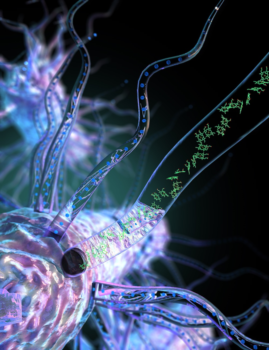
Ideally, injectable or implantable medical devices should not only be small and electrically functional, they should be soft, like the body tissues with which they interact. Scientists from two UChicago labs set out to see if they could design a material with all three of those properties.
The material they came up with, published online June 27, 2016, in Nature Materials, forms the basis of an ingenious light-activated injectable device that could eventually be used to stimulate nerve cells and manipulate the behavior of muscles and organs.
“Most traditional materials for implants are very rigid and bulky, especially if you want to do electrical stimulation,” said Bozhi Tian, an assistant professor in chemistry whose lab collaborated with that of neuroscientist Francisco Bezanilla on the research.
The new material, in contrast, is soft and tiny — particles just a few micrometers in diameter (far less than the width of a human hair) that disperse easily in a saline solution so they can be injected. The particles also degrade naturally inside the body after a few months, so no surgery would be needed to remove them.
A July 1, 2016 University of Chicago news release (also on EurekAlert) by , which originated the news item, provides more detail,
Each particle is built of two types of silicon that together form a structure full of nano-scale pores, like a tiny sponge. And like a sponge, it is squishy — a hundred to a thousand times less rigid than the familiar crystalline silicon used in transistors and solar cells. “It is comparable to the rigidity of the collagen fibers in our bodies,” said Yuanwen Jiang, Tian’s graduate student. “So we’re creating a material that matches the rigidity of real tissue.”
The material constitutes half of an electrical device that creates itself spontaneously when one of the silicon particles is injected into a cell culture, or, eventually, a human body. The particle attaches to a cell, making an interface with the cell’s plasma membrane. Those two elements together — cell membrane plus particle — form a unit that generates current when light is shined on the silicon particle.
“You don’t need to inject the entire device; you just need to inject one component,” João L. Carvalho-de-Souza , Bezanilla’s postdoc said. “This single particle connection with the cell membrane allows sufficient generation of current that could be used to stimulate the cell and change its activity. After you achieve your therapeutic goal, the material degrades naturally. And if you want to do therapy again, you do another injection.”
The scientists built the particles using a process they call nano-casting. They fabricate a silicon dioxide mold composed of tiny channels — “nano-wires” — about seven nanometers in diameter (less than 10,000 times smaller than the width of a human hair) connected by much smaller “micro-bridges.” Into the mold they inject silane gas, which fills the pores and channels and decomposes into silicon.
And this is where things get particularly cunning. The scientists exploit the fact the smaller an object is, the more the atoms on its surface dominate its reactions to what is around it. The micro-bridges are minute, so most of their atoms are on the surface. These interact with oxygen that is present in the silicon dioxide mold, creating micro-bridges made of oxidized silicon gleaned from materials at hand. The much larger nano-wires have proportionately fewer surface atoms, are much less interactive, and remain mostly pure silicon. [I have a note regarding ‘micro’ and ‘nano’ later in this posting.]
“This is the beauty of nanoscience,” Jiang said. “It allows you to engineer chemical compositions just by manipulating the size of things.”
Web-like nanostructure
Finally, the mold is dissolved. What remains is a web-like structure of silicon nano-wires connected by micro-bridges of oxidized silicon that can absorb water and help increase the structure’s softness. The pure silicon retains its ability to absorb light.
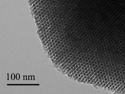
Transmission electron microscopy image shows an ordered nanowire array. The 100-nanometer scale bar is 1,000 times narrower than a hair. Courtesy of
Tian Lab
The scientists have added the particles onto neurons in culture in the lab, shone light on the particles, and seen current flow into the neurons which activates the cells. The next step is to see what happens in living animals. They are particularly interested in stimulating nerves in the peripheral nervous system that connect to organs. These nerves are relatively close to the surface of the body, so near-infra-red wavelength light can reach them through the skin.
Tian imagines using the light-activated devices to engineer human tissue and create artificial organs to replace damaged ones. Currently, scientists can make engineered organs with the correct form but not the ideal function.
To get a lab-built organ to function properly, they will need to be able to manipulate individual cells in the engineered tissue. The injectable device would allow a scientist to do that, tweaking an individual cell using a tightly focused beam of light like a mechanic reaching into an engine and turning a single bolt. The possibility of doing this kind of synthetic biology without genetic engineering [emphasis mine] is enticing.
“No one wants their genetics to be altered,” Tian said. “It can be risky. There’s a need for a non-genetic system that can still manipulate cell behavior. This could be that kind of system.”
Tian’s graduate student Yuanwen Jiang did the material development and characterization on the project. The biological part of the collaboration was done in the lab of Francisco Bezanilla, the Lillian Eichelberger Cannon Professor of Biochemistry and Molecular Biology, by postdoc João L. Carvalho-de-Souza. They were, said Tian, the “heroes” of the work.
I was a little puzzled about the use of the word ‘micro’ in a context suggesting it was smaller than something measured at the nanoscale. Dr. Tian very kindly cleared up my confusion with this response in a July 4, 2016 email,
In fact, the definition of ‘micro’ and ’nano’ have been quite ambiguous in literature. For example, microporous materials (e.g., zeolite) usually refer to materials with pore sizes of less than 2 nm — this is defined based on IUPAC [International Union of Pure and Applied Chemistry] definition (http://goldbook.iupac.org/M03853.html). We used ‘micro-bridges’ because they come from the ‘micropores’ in the original template.
Thank you Dr. Tian for that very clear reply and Steve Koppes for forwarding my request to Dr. Tian!
Here’s a link to and a citation for the paper,
Heterogeneous silicon mesostructures for lipid-supported bioelectric interfaces by Yuanwen Jiang, João L. Carvalho-de-Souza, Raymond C. S. Wong, Zhiqiang Luo, Dieter Isheim, Xiaobing Zuo, Alan W. Nicholls, Il Woong Jung, Jiping Yue, Di-Jia Liu, Yucai Wang, Vincent De Andrade, Xianghui Xiao, Luizetta Navrazhnykh, Dara E. Weiss, Xiaoyang Wu, David N. Seidman, Francisco Bezanilla, & Bozhi Tian. Nature Materials (2016) doi:10.1038/nmat4673 Published online 27 June 2016
This paper is behind a paywall.
I gather animal testing will be the next step as they continue to develop this exciting technology. Good luck!