Tag Archives: Nathaniel M. Gabor

Better performing solar cells with newly discovered property of pristine graphene

Light-harvesting devices—I like that better than solar cells or the like but I think that the term serves as a category rather than a name/label for a specific device. Enough musing. A December 17, 2018 news item on Nanowerk describes the latest about graphene and light-harvesting devices (Note: A link has been removed,

An international research team, co-led by a physicist at the University of California, Riverside, has discovered a new mechanism for ultra-efficient charge and energy flow in graphene, opening up opportunities for developing new types of light-harvesting devices.

The researchers fabricated pristine graphene — graphene with no impurities — into different geometric shapes, connecting narrow ribbons and crosses to wide open rectangular regions. They found that when light illuminated constricted areas, such as the region where a narrow ribbon connected two wide regions, they detected a large light-induced current, or photocurrent.

The finding that pristine graphene can very efficiently convert light into electricity could lead to the development of efficient and ultrafast photodetectors — and potentially more efficient solar panels.

A December 14, 2018 University of California at Riverside (UCR) news release by Iqbal Pittalwala (also on EurekAlert but published Dec. 17, 2018), which originated the news item,gives a brief description of graphene while adding context for this research,


Graphene, a 1-atom thick sheet of carbon atoms arranged in a hexagonal lattice, has many desirable material properties, such as high current-carrying capacity and thermal conductivity. In principle, graphene can absorb light at any frequency, making it ideal material for infrared and other types of photodetection, with wide applications in bio-sensing, imaging, and night vision.

In most solar energy harvesting devices, a photocurrent arises only in the presence of a junction between two dissimilar materials, such as “p-n” junctions, the boundary between two types of semiconductor materials. The electrical current is generated in the junction region and moves through the distinct regions of the two materials.

“But in graphene, everything changes,” said Nathaniel Gabor, an associate professor of physics at UCR, who co-led the research project. “We found that photocurrents may arise in pristine graphene under a special condition in which the entire sheet of graphene is completely free of excess electronic charge. Generating the photocurrent requires no special junctions and can instead be controlled, surprisingly, by simply cutting and shaping the graphene sheet into unusual configurations, from ladder-like linear arrays of contacts, to narrowly constricted rectangles, to tapered and terraced edges.”

Pristine graphene is completely charge neutral, meaning there is no excess electronic charge in the material. When wired into a device, however, an electronic charge can be introduced by applying a voltage to a nearby metal. This voltage can induce positive charge, negative charge, or perfectly balance negative and positive charges so the graphene sheet is perfectly charge neutral.

“The light-harvesting device we fabricated is only as thick as a single atom,” Gabor said. “We could use it to engineer devices that are semi-transparent. These could be embedded in unusual environments, such as windows, or they could be combined with other more conventional light-harvesting devices to harvest excess energy that is usually not absorbed. Depending on how the edges are cut to shape, the device can give extraordinarily different signals.”

The research team reports this first observation of an entirely new physical mechanism — a photocurrent generated in charge-neutral graphene with no need for p-n junctions — in Nature Nanotechnology today [Dec. 17, 2018].

Previous work by the Gabor lab showed a photocurrent in graphene results from highly excited “hot” charge carriers. When light hits graphene, high-energy electrons relax to form a population of many relatively cooler electrons, Gabor explained, which are subsequently collected as current. Even though graphene is not a semiconductor, this light-induced hot electron population can be used to generate very large currents.

“All of this behavior is due to graphene’s unique electronic structure,” he said. “In this ‘wonder material,’ light energy is efficiently converted into electronic energy, which can subsequently be transported within the material over remarkably long distances.”

He explained that, about a decade ago, pristine graphene was predicted to exhibit very unusual electronic behavior: electrons should behave like a liquid, allowing energy to be transferred through the electronic medium rather than by moving charges around physically.
“But despite this prediction, no photocurrent measurements had been done on pristine graphene devices — until now,” he said.

The new work on pristine graphene shows electronic energy travels great distances in the absence of excess electronic charge.

The research team has found evidence that the new mechanism results in a greatly enhanced photoresponse in the infrared regime with an ultrafast operation speed.
“We plan to further study this effect in a broad range of infrared and other frequencies, and measure its response speed,” said first author Qiong Ma, a postdoctoral associate in physics at the Massachusetts Institute of Technology, or MIT.

The researchers have provided an image illustrating their work,
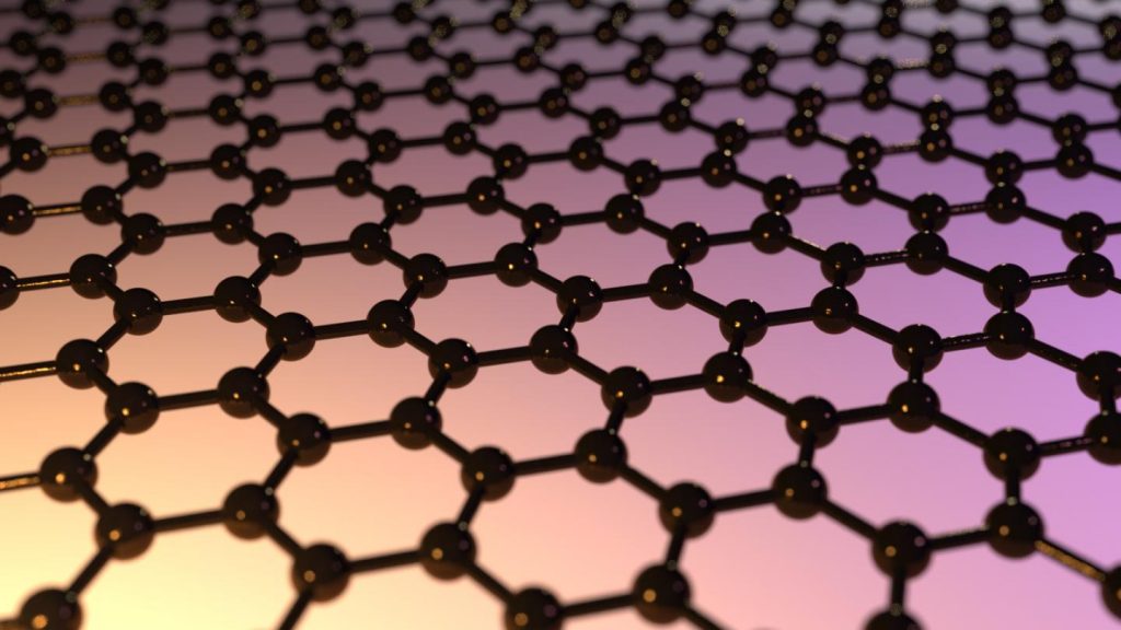
Caption: Shining light on graphene: Although graphene has been studied vigorously for more than a decade, new measurements on high-performance graphene devices have revealed yet another unusual property. In ultra-clean graphene sheets, energy can flow over great distances, giving rise to an unprecedented response to light. Credit: Max Grossnickle and QMO Labs, UC Riverside.

Here’s a link to and a citation for the paper,

Giant intrinsic photoresponse in pristine graphene by Qiong Ma, Chun Hung Lui, Justin C. W. Song, Yuxuan Lin, Jian Feng Kong, Yuan Cao, Thao H. Dinh, Nityan L. Nair, Wenjing Fang, Kenji Watanabe, Takashi Taniguchi, Su-Yang Xu, Jing Kong, Tomás Palacios, Nuh Gedik, Nathaniel M. Gabor, & Pablo Jarillo-Herrero. Nature Nanotechnology (2018) Published 17 December 2018 DOI: https://doi.org/10.1038/s41565-018-0323-8

This paper is behind a paywall.

Electron quantum materials, a new field in nanotechnology?

Physicists name and codify new field in nanotechnology: ‘electron quantum metamaterials’

UC Riverside’s Nathaniel Gabor and colleague formulate a vision for the field in a perspective article

Courtesy: University of California at Riverside

Bravo to whomever put the image of a field together together with a subhead that includes the phrases ‘vision for a field’ and ‘perspective article’. It’s even better if you go to the November 5, 2018 University of California at Riverside (UCR) news release (also on EurekAlert) by Iqbal Pittalwala to see the original format,

When two atomically thin two-dimensional layers are stacked on top of each other and one layer is made to rotate against the second layer, they begin to produce patterns — the familiar moiré patterns — that neither layer can generate on its own and that facilitate the passage of light and electrons, allowing for materials that exhibit unusual phenomena. For example, when two graphene layers are overlaid and the angle between them is 1.1 degrees, the material becomes a superconductor.

“It’s a bit like driving past a vineyard and looking out the window at the vineyard rows. Every now and then, you see no rows because you’re looking directly along a row,” said Nathaniel Gabor, an associate professor in the Department of Physics and Astronomy at the University of California, Riverside. “This is akin to what happens when two atomic layers are stacked on top of each other. At certain angles of twist, everything is energetically allowed. It adds up just right to allow for interesting possibilities of energy transfer.”

This is the future of new materials being synthesized by twisting and stacking atomically thin layers, and is still in the “alchemy” stage, Gabor added. To bring it all under one roof, he and physicist Justin C. W. Song of Nanyang Technological University, Singapore, have proposed this field of research be called “electron quantum metamaterials” and have just published a perspective article in Nature Nanotechnology.

“We highlight the potential of engineering synthetic periodic arrays with feature sizes below the wavelength of an electron. Such engineering allows the electrons to be manipulated in unusual ways, resulting in a new range of synthetic quantum metamaterials with unconventional responses,” Gabor said.

Metamaterials are a class of material engineered to produce properties that do not occur naturally. Examples include optical cloaking devices and super-lenses akin to the Fresnel lens that lighthouses use. Nature, too, has adopted such techniques – for example, in the unique coloring of butterfly wings – to manipulate photons as they move through nanoscale structures.

“Unlike photons that scarcely interact with each other, however, electrons in subwavelength structured metamaterials are charged, and they strongly interact,” Gabor said. “The result is an enormous variety of emergent phenomena and radically new classes of interacting quantum metamaterials.”

Gabor and Song were invited by Nature Nanotechnology to write a review paper. But the pair chose to delve deeper and lay out the fundamental physics that may explain much of the research in electron quantum metamaterials. They wrote a perspective paper instead that envisions the current status of the field and discusses its future.

“Researchers, including in our own labs, were exploring a variety of metamaterials but no one had given the field even a name,” said Gabor, who directs the Quantum Materials Optoelectronics lab at UCR. “That was our intent in writing the perspective. We are the first to codify the underlying physics. In a way, we are expressing the periodic table of this new and exciting field. It has been a herculean task to codify all the work that has been done so far and to present a unifying picture. The ideas and experiments have matured, and the literature shows there has been rapid progress in creating quantum materials for electrons. It was time to rein it all in under one umbrella and offer a road map to researchers for categorizing future work.”

In the perspective, Gabor and Song collect early examples in electron metamaterials and distil emerging design strategies for electronic control from them. They write that one of the most promising aspects of the new field occurs when electrons in subwavelength-structure samples interact to exhibit unexpected emergent behavior.

“The behavior of superconductivity in twisted bilayer graphene that emerged was a surprise,” Gabor said. “It shows, remarkably, how electron interactions and subwavelength features could be made to work together in quantum metamaterials to produce radically new phenomena. It is examples like this that paint an exciting future for electronic metamaterials. Thus far, we have only set the stage for a lot of new work to come.”

Gabor, a recipient of a Cottrell Scholar Award and a Canadian Institute for Advanced Research Azrieli Global Scholar Award, was supported by the Air Force Office of Scientific Research Young Investigator Program and a National Science Foundation Division of Materials Research CAREER award.

There is a video illustrating the ideas which is embedded in a November 5, 2018 news item on phys.oirg,


Here’s a link to and a citation for the ‘perspective’ paper,

Electron quantum metamaterials in van der Waals heterostructures by Justin C. W. Song & Nathaniel M. Gabor. Nature Nanotechnology, volume 13, pages986–993 (2018) DOI: https://doi.org/10.1038/s41565-018-0294-9 Published: 05 November 2018

This paper is behind a paywall.