Tag Archives: nickel

Replacing nanotechnology-enabled oil spill solutions with dog fur?

Coincidentally or not, this research from Australia was announced a little more than a month after reports of a major oil spill in the Russian Arctic. A July 10, 2020 news item on phys.org announces a new technology for mopping up oil spills (Note: Links have been removed),

Oil spill disasters on land cause long-term damage for communities and the natural environment, polluting soils and sediments and contaminating groundwater.

Current methods using synthetic sorbent materials can be effective for cleaning up oil spills, but these materials are often expensive and generate large volumes of non-biodegradable plastic wastes. Now the first comparison of natural-origin sorbent materials for land-based oil spills, including peat moss, recycled human hair, and dog fur, shows that sustainable, cheaper and biodegradable options can be developed.

The University of Technology Sydney (UTS) project found that dog fur and human hair products—recycled from salon wastes and dog groomers—can be just as good as synthetic fabrics at cleaning up crude oil spills on hard land surfaces like highway roads, pavement, and sealed concrete floors. Polypropylene, a plastic, is a widely-used fabric used to clean up oil spills in aquatic environments.

A July 9, 2020 Univesity of Technology Sydney press release on EurekAlert completes the story,

“Dog fur in particular was surprisingly good at oil spill clean-up, and felted mats from human hair and fur were very easy to apply and remove from the spills.” lead author of the study, UTS Environmental Scientist Dr Megan Murray, said. Dr Murray investigates environmentally-friendly solutions for contamination and leads The Phyto Lab research group at UTS School of Life Sciences.

“This is a very exciting finding for land managers who respond to spilled oil from trucks, storage tanks, or leaking oil pipelines. All of these land scenarios can be treated effectively with sustainable-origin sorbents,” she said.

The sorbents tested included two commercially-available products, propylene and loose peat moss, as well as sustainable-origin prototypes including felted mats made of dog fur and human hair. Prototype oil-spill sorbent booms filled with dog fur and human hair were also tested. Crude oil was used to replicate an oil spill. The results of the study are published in Environments.

The research team simulated three types of land surfaces; non-porous hard surfaces, semi-porous surfaces, and sand, to recreate common oil-spill scenarios.

“We found that loose peat moss is not as effective at cleaning up oil spills on land compared to dog fur and hair products, and it is not useful at all for sandy environments.” Dr Murray said.

“Based on this research, we recommend peat moss is no longer used for this purpose. Given that peat moss is a limited resource and harvesting it requires degrading wetland ecosystems, we think this is a very important finding.” she said.

The research concluded that, for now, sandy environments like coastal beaches can still benefit from the use of polypropylene sorbents, but further exploration of sustainable-origin sorbents is planned.

The researchers say that future applications from the research include investigating felted mats of sustainable-origin sorbents for river bank stabilisation, [emphases mine] as well as the removal of pollutants from flowing polluted waters, similar to existing membrane technology.

Here’s a link to and a citation for the study,

Decontaminating Terrestrial Oil Spills: A Comparative Assessment of Dog Fur, Human Hair, Peat Moss and Polypropylene Sorbents by Megan L. Murray, Soeren M. Poulsen and Brad R. Murray. Environments 2020, 7(7), 52; DOI: https://doi.org/10.3390/environments7070052 Published: 8 July 2020 (This article belongs to the Special Issue Pollution Prevention/Environmental Sustainability for Industry)

This paper is open access.

As for the Russian oil spill

A June 4, 2020 British Broadcasting Corporation (BBC) news online article outlines the situation regarding the oil spill and the steps being taken to deal with it,

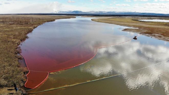
Russia’s President Vladimir Putin has declared a state of emergency after 20,000 tonnes of diesel oil leaked into a river within the Arctic Circle.

The spill happened when a fuel tank at a power plant near the Siberian city of Norilsk collapsed last Friday [May 29, 2020].

The power plant’s director Vyacheslav Starostin has been taken into custody until 31 July, but not yet charged.

The plant is owned by a subsidiary of Norilsk Nickel, which is the world’s leading nickel and palladium producer.

The Russian Investigative Committee (SK) has launched a criminal case over the pollution and alleged negligence, as there was reportedly a two-day delay in informing the Moscow authorities about the spill.

Ground subsidence beneath the fuel storage tanks is believed to have caused the spill. Arctic permafrost has been melting in exceptionally warm weather [more information about the weather towards the end of this posting] for this time of year.

Russian Minister for Emergencies Yevgeny Zinichev told Mr Putin that the Norilsk plant had spent two days trying to contain the spill, before alerting his ministry.

The leaked oil drifted some 12km (7.5 miles) from the accident site, turning long stretches of the Ambarnaya river crimson red.

The leaked diesel oil drifted some 12km (7.5 miles) from the site of the accident [downloaded from https://www.bbc.com/news/world-europe-52915807]

Getting back to the June 4, 2020 British Broadcasting Corporation (BBC) news online article,

“Why did government agencies only find out about this two days [May 29, 2020?) after the fact?” he asked the subsidiary’s chief, Sergei Lipin. “Are we going to learn about emergency situations from social media?”

The region’s governor, Alexander Uss, had earlier told President Putin that he became aware of the oil spill on Sunday [May 31, 2020] after “alarming information appeared in social media”.

The spill has contaminated a 350 sq km (135 sq mile) area, state media report.

The state of emergency means extra forces are going to the area to assist with the clean-up operation.

The accident is believed to be the second largest in modern Russian history in terms of volume, an expert from the World Wildlife Fund, Alexei Knizhnikov, told the AFP [Agence France Presse] news agency.

The incident has prompted stark warnings from environmental groups, who say the scale of the spill and geography of the river mean it will be difficult to clean up.

Greenpeace has compared it to the 1989 Exxon Valdez disaster in Alaska.

Oleg Mitvol, former deputy head of Russia’s environmental watchdog Rosprirodnadzor, said there had “never been such an accident in the Arctic zone”.

He said the clean-up could cost 100bn roubles (£1.2bn; $1.5bn) and take between five and 10 years.

Minister of Natural Resources Dmitry Kobylkin warned against trying to burn off such a vast quantity of fuel oil.

He proposed trying to dilute the oil with reagents. Only the emergencies ministry with military support could deal with the pollution, he said.

Barges with booms could not contain the slick because the Ambarnaya river was too shallow, he warned.

He suggested pumping the oil on to the adjacent tundra, although President Putin added: “The soil there is probably saturated [with oil] already.”

An update of the situation can be found in a July 8, 2020 Canadian Broadcasting Corporation (CBC) article (issued by Thomson Reuters),

Russia’s environmental watchdog has asked a power subsidiary of Russian mining giant Norilsk Nickel to pay almost 148 billion rubles, or $2.8 billion Cdn, in damages over an Arctic fuel spill in Siberia.

Rosprirodnadzor, the Federal Service for Supervision of Use of Natural Resources, said in a statement on Monday [July 8, 2020] that it had already sent a request for “voluntary compensation” to the subsidiary, NTEK, after calculating the damage caused by the May 29 [2020] fuel spill.

Norilsk Nickel’s Moscow-listed shares fell by 3 per cent after the watchdog’s statement.

A fuel tank at the power plant lost pressure and released 21,000 tonnes of diesel into rivers and subsoil near the city of Norilsk, 2,900 kilometres northeast of Moscow. Russian President Vladimir Putin subsequently declared a state of emergency in the region, and investigators detained three staff at the power plant.

Norilsk, a remote city of 180,000 people situated 300 kilometres inside the Arctic Circle, is built around Norilsk Nickel, the world’s leading nickel and palladium producer, and has a reputation for its pollution.

Rosprirodnadzor said the damages included the cost for nearby water bodies, estimated at 147.05 billion rubles, $2.8 billion Cdn, and for subsoil, estimated at 738.62 million roubles, $14 million Cdn.

I can’t find any August 2020 updates for the oil spill situation in Russia. (Note: There is now an oil spill in a ecologically sensitive region near Mauritius; see August 13, 2020 news item on CBC news online website.)

Exceptionally warm weather

The oil spill isn’t the only problem in the Arctic.Here’s more from a June 23, 2020 article by Matt Simon for Wired magazine (Note: A link has been removed),

On Saturday [June 20, 2020], the residents of Verkhoyansk, Russia, marked the first day of summer with 100 degree Fahrenheit temperatures. Not that they could enjoy it, really, as Verkhoyansk is in Siberia, hundreds of miles from the nearest beach. That’s much, much hotter than towns inside the Arctic Circle usually get. That 100 degrees appears to be a record, well above the average June high temperature of 68 degrees. Yet it’s likely the people of Verkhoyansk will see that record broken again in their lifetimes: The Arctic is warming twice as fast as the rest of the planet—if not faster—creating ecological chaos for the plants and animals that populate the north.

“The events over the weekend—in the last few weeks, really—with the heatwave in Siberia, all are unprecedented in terms of the magnitude of the extremes in temperature,” says Sophie Wilkinson, a wildfire scientist at McMaster University who studies northern peat fires, which themselves have grown unusually frequent in recent years as temperatures climb.

The Arctic’s extreme warming, known as Arctic amplification or polar amplification, may be due to three factors. One, the region’s reflectivity, or albedo—how much light it bounces back into space—is changing as the world warms. “What we’ve been seeing over the last 30 years is some relatively dramatic declines in sea ice in the summertime,” says University of Edinburgh global change ecologist Isla Myers-Smith, who studies the Arctic.

Since ice is white, it reflects the sun’s energy, something you’re already probably familiar with when it comes to staying cool in the summer. If you had to pick the color of T-shirt to wear when going hiking on a hot day, she says, “most of us would pick the white T-shirt, because that’s going to reflect the sun’s heat off of our back.” Similarly, Myers-Smith says, “If the sea ice melts in the Arctic, that will remove that white surface off of the ocean, and what will be exposed is this darker ocean surface that will absorb more of the sun’s heat.”

If you’re interested in the environmental consequences of the warming of the Arctic, this is a very good article.

Finishing up, I wish the clean-up crews (in Russia and near Mauritius) all the best as they work in the midst of a pandemic, as well as, an environmental disaster (both the oil spill and the warming of the Arctic).

Make electricity by flowing water over nanolayers of metal

Scientists at Northwestern University (Chicago, Illinois) and the California Institute of Technology (CalTech) have developed what could be a more sustainable way to produce electricity. From a July 31, 2019 news item on Nanowerk,

Scientists from Northwestern University and Caltech have produced electricity by simply flowing water over extremely thin layers of inexpensive metals, including iron, that have oxidized. These films represent an entirely new way of generating electricity and could be used to develop new forms of sustainable power production.

A July 31, 2019 Northwester University news release (also on EurekAlert) by Megan Fellman, which originated the news item, provides details that suggest this discovery could prove beneficial in medical implants, as well as, in solar cells,

The films have a conducting metal nanolayer (10 to 20 nanometers thick) that is insulated with an oxide layer (2 nanometers thick). Current is generated when pulses of rainwater and ocean water alternate and move across the nanolayers. The difference in salinity drags the electrons along in the metal below.

“It’s the oxide layer over the nanometal that really makes this device go,” said Franz M. Geiger, the Dow Professor of Chemistry in Northwestern’s Weinberg College of Arts and Sciences. “Instead of corrosion, the presence of the oxides on the right metals leads to a mechanism that shuttles electrons.”

The films are transparent, a feature that could be taken advantage of in solar cells. The researchers intend to study the method using other ionic liquids, including blood. Developments in this area could lead to use in stents and other implantable devices.

“The ease of scaling up the metal nanolayer to large areas and the ease with which plastics can be coated gets us to three-dimensional structures where large volumes of liquids can be used,” Geiger said. “Foldable designs that fit, for instance, into a backpack are a possibility as well. Given how transparent the films are, it’s exciting to think about coupling the metal nanolayers to a solar cell or coating the outside of building windows with metal nanolayers to obtain energy when it rains.”

The study, titled “Energy Conversion via Metal Nanolayers,” was published this week [on July 29, 2019] in the journal Proceedings of the National Academy of Sciences (PNAS).

Geiger is the study’s corresponding author; his Northwestern team conducted the experiments. Co-author Thomas Miller, professor of chemistry at Caltech, led a team that conducted atomistic simulations to study the device’s behavior at the atomic level.

The new method produces voltages and currents comparable to graphene-based devices reported to have efficiencies of around 30% — similar to other approaches under investigation (carbon nanotubes and graphene) but with a single-step fabrication from earth-abundant elements instead of multistep fabrication. This simplicity allows for scalability, rapid implementation and low cost. Northwestern has filed for a provisional patent.

Of the metals studied, the researchers found that iron, nickel and vanadium worked best. They tested a pure rust sample as a control experiment; it did not produce a current.

The mechanism behind the electricity generation is complex, involving ion adsorption and desorption, but it essentially works like this: The ions present in the rainwater/saltwater attract electrons in the metal beneath the oxide layer; as the water flows, so do those ions, and through that attractive force, they drag the electrons in the metal along with them, generating an electrical current.

“There are interesting prospects for a variety of energy and sustainability applications, but the real value is the new mechanism of oxide-metal electron transfer,” Geiger said. “The underlying mechanism appears to involve various oxidation states.”

The team used a process called physical vapor deposition (PVD), which turns normally solid materials into a vapor that condenses on a desired surface. PVD allowed them to deposit onto glass metal layers only 10 to 20 nanometers thick. An oxide layer then forms spontaneously in air. It grows to a thickness of 2 nanometers and then stops growing.

“Thicker films of metal don’t succeed — it’s a nano-confinement effect,” Geiger said. “We have discovered the sweet spot.”

When tested, the devices generated several tens of millivolts and several microamps per centimeter squared.

“For perspective, plates having an area of 10 square meters each would generate a few kilowatts per hour — enough for a standard U.S. home,” Miller said. “Of course, less demanding applications, including low-power devices in remote locations, are more promising in the near term.”

Here’s a link to and a citation for the paper,

Energy conversion via metal nanolayers by Mavis D. Boamah, Emilie H. Lozier, Jeongmin Kim, Paul E. Ohno, Catherine E. Walker, Thomas F. Miller III, and Franz M. Geiger. PNAS DOI: https://doi.org/10.1073/pnas.1906601116 First published July 29, 2019

This paper is behind a paywall.

Bristly hybrid materials

Caption: [Image 1] A carbon fiber covered with a spiky forest of NiCoHC nanowires. Credit: All images reproduced from reference 1 under a Creative Commons Attribution 4.0 International License© 2018 KAUST

It makes me think of small, cuddly things like cats and dogs but it’s not. From an August 7, 2018 King Abdullah University of Science and Technology (KAUST; Saudi Arabia) news release (also published on August 12, 2018 on EurekAlert),

By combining multiple nanomaterials into a single structure, scientists can create hybrid materials that incorporate the best properties of each component and outperform any single substance. A controlled method for making triple-layered hollow nanostructures has now been developed at KAUST. The hybrid structures consist of a conductive organic core sandwiched between layers of electrocatalytically active metals: their potential uses range from better battery electrodes to renewable fuel production.

Although several methods exist to create two-layer materials, making three-layered structures has proven much more difficult, says Peng Wang from the Water Desalination and Reuse Center who co-led the current research with Professor Yu Han, member of the Advanced Membranes and Porous Materials Center at KAUST. The researchers developed a new, dual-template approach, explains Sifei Zhuo, a postdoctoral member of Wang’s team.

The researchers grew their hybrid nanomaterial directly on carbon paper–a mat of electrically conductive carbon fibers. They first produced a bristling forest of nickel cobalt hydroxyl carbonate (NiCoHC) nanowires onto the surface of each carbon fiber (image 1). Each tiny inorganic bristle was coated with an organic layer called hydrogen substituted graphdiyne (HsGDY) (image 2 [not included here]).

Next was the key dual-template step. When the team added a chemical mixture that reacts with the inner NiCoHC, the HsGDY acted as a partial barrier. Some nickel and cobalt ions from the inner layer diffused outward, where they reacted with thiomolybdate from the surrounding solution to form the outer nickel-, cobalt-co-doped MoS2 (Ni,Co-MoS2) layer. Meanwhile, some sulfur ions from the added chemicals diffused inwards to react with the remaining nickel and cobalt. The resulting substance (image 3 [not included here]) had the structure Co9S8, Ni3S2@HsGDY@Ni,Co-MoS2, in which the conductive organic HsGDY layer is sandwiched between two inorganic layers (image 4 [not included here]).

The triple layer material showed good performance at electrocatalytically breaking up water molecules to generate hydrogen, a potential renewable fuel. The researchers also created other triple-layer materials using the dual-template approach

“These triple-layered nanostructures hold great potential in energy conversion and storage,” says Zhuo. “We believe it could be extended to serve as a promising electrode in many electrochemical applications, such as in supercapacitors and sodium-/lithium-ion batteries, and for use in water desalination.”

Here’s a link to and a citation for the paper,

Dual-template engineering of triple-layered nanoarray electrode of metal chalcogenides sandwiched with hydrogen-substituted graphdiyne by Sifei Zhuo, Yusuf Shi, Lingmei Liu, Renyuan Li, Le Shi, Dalaver H. Anjum, Yu Han, & Peng Wang. Nature Communicationsvolume 9, Article number: 3132 (2018) DOI: https://doi.org/10.1038/s41467-018-05474-0 Published 07 August 2018

This paper is open access.


Thin-film electronic stickers for the Internet of Things (IoT)

This research is from Purdue University (Indiana, US) and the University of Virginia (US) increases and improves the interactivity between objects in what’s called the Internet of Things (IoT).

Caption: Electronic stickers can turn ordinary toy blocks into high-tech sensors within the ‘internet of things.’ Credit: Purdue University image/Chi Hwan Lee

From a July 16, 2018 news item on ScienceDaily,

Billions of objects ranging from smartphones and watches to buildings, machine parts and medical devices have become wireless sensors of their environments, expanding a network called the “internet of things.”

As society moves toward connecting all objects to the internet — even furniture and office supplies — the technology that enables these objects to communicate and sense each other will need to scale up.

Researchers at Purdue University and the University of Virginia have developed a new fabrication method that makes tiny, thin-film electronic circuits peelable from a surface. The technique not only eliminates several manufacturing steps and the associated costs, but also allows any object to sense its environment or be controlled through the application of a high-tech sticker.

Eventually, these stickers could also facilitate wireless communication. …

A July 16, 2018 University of Purdue news release (also on EurekAlert), which originated the news item, explains more,

“We could customize a sensor, stick it onto a drone, and send the drone to dangerous areas to detect gas leaks, for example,” said Chi Hwan Lee, Purdue assistant professor of biomedical engineering and mechanical engineering.

Most of today’s electronic circuits are individually built on their own silicon “wafer,” a flat and rigid substrate. The silicon wafer can then withstand the high temperatures and chemical etching that are used to remove the circuits from the wafer.

But high temperatures and etching damage the silicon wafer, forcing the manufacturing process to accommodate an entirely new wafer each time.

Lee’s new fabrication technique, called “transfer printing,” cuts down manufacturing costs by using a single wafer to build a nearly infinite number of thin films holding electronic circuits. Instead of high temperatures and chemicals, the film can peel off at room temperature with the energy-saving help of simply water.

“It’s like the red paint on San Francisco’s Golden Gate Bridge – paint peels because the environment is very wet,” Lee said. “So in our case, submerging the wafer and completed circuit in water significantly reduces the mechanical peeling stress and is environmentally-friendly.”

A ductile metal layer, such as nickel, inserted between the electronic film and the silicon wafer, makes the peeling possible in water. These thin-film electronics can then be trimmed and pasted onto any surface, granting that object electronic features.

Putting one of the stickers on a flower pot, for example, made that flower pot capable of sensing temperature changes that could affect the plant’s growth.

Lee’s lab also demonstrated that the components of electronic integrated circuits work just as well before and after they were made into a thin film peeled from a silicon wafer. The researchers used one film to turn on and off an LED light display.

“We’ve optimized this process so that we can delaminate electronic films from wafers in a defect-free manner,” Lee said.

This technology holds a non-provisional U.S. patent. The work was supported by the Purdue Research Foundation, the Air Force Research Laboratory (AFRL-S-114-054-002), the National Science Foundation (NSF-CMMI-1728149) and the University of Virginia.

The researchers have provided a video,

Here’s a link to and a citation for the paper,

Wafer-recyclable, environment-friendly transfer printing for large-scale thin-film nanoelectronics by Dae Seung Wie, Yue Zhang, Min Ku Kim, Bongjoong Kim, Sangwook Park, Young-Joon Kim, Pedro P. Irazoqui, Xiaolin Zheng, Baoxing Xu, and Chi Hwan Lee.
PNAS July 16, 2018 201806640 DOI: https://doi.org/10.1073/pnas.1806640115
published ahead of print July 16, 2018

This paper is behind a paywall.

Dexter Johnson provides some context in his July 25, 2018 posting on the Nanoclast blog (on the IEEE [Institute of Electronic and Electrical Engineers] website), Note: A link has been removed,

The Internet of Things (IoT), the interconnection of billions of objects and devices that will be communicating with each other, has been the topic of many futurists’ projections. However, getting the engineering sorted out with the aim of fully realizing the myriad visions for IoT is another story. One key issue to address: How do you get the electronics onto these devices efficiently and economically?

A team of researchers from Purdue University and the University of Virginia has developed a new manufacturing process that could make equipping a device with all the sensors and other electronics that will make it Internet capable as easily as putting a piece of tape on it.

… this new approach makes use of a water environment at room temperature to control the interfacial debonding process. This allows clean, intact delamination of prefabricated thin film devices when they’re pulled away from the original wafer.

The use of mechanical peeling in water rather than etching solution provides a number of benefits in the manufacturing scheme. Among them are simplicity, controllability, and cost effectiveness, says Chi Hwan Lee, assistant professor at Purdue University and coauthor of the paper chronicling the research.

If you have the time, do read Dexter’s piece. He always adds something that seems obvious in retrospect but wasn’t until he wrote it.

Golden nanoglue

This starts out as a graphene story before taking an abrupt turn. From a June 5, 2018 news item on Nanowerk,

Graphene has undoubtedly been the most popular research subject of nanotechnology during recent years. Made of pure carbon, this material is in principle easy to manufacture: take ordinary graphite and peel one layer off with Scotch tape. The material thus obtained is two-dimensional, yielding unique properties, different from those in three-dimensional materials.

Graphene, however, lacks one important property, semiconductivity, which complicates its usage in electronics applications. Scientists have therefore started the quest of other two-dimensional materials with this desired property.

Molybdenum disulfide, MoS2 is among the most promising candidates. Like graphene, MoS2 consists of layers, interacting weakly with one another. In addition to being a semiconductor, the semiconducting properties of MoS2 change depending on the number of atomic layers.

A June 5, 2018 University of Oulu press release, which originated the news item,  gives more detail about the work,

For the one or few layer MoS2 to be useful in applications, one must be able to join it to other components. What is thus needed is such a metallic conductor that electric current can easily flow between the conductor and the semiconductor. In the case of MoS2, a promising conductor is provided by nickel, which also has other desired properties from the applications point of view.

However, an international collaboration, led by the Nano and molecular systems research unit at the University of Oulu has recently discovered that nanoparticles made of nickel do not attach to MoS2. One needs gold, which ‘glues’ the conductor and the component together. Says docent Wei Cao of NANOMO: “The synthesis is performed through a sonochemical method.” Sonochemistry is a method where chemical reactions are established using ultrasound. NANOMO scientist Xinying Shi adds: “The semiconductor and metal can be bridged either by the crystallized gold nanoparticles, or by the newly formed MoS2-Au-Ni ternary alloy.”

The nanojunction so established has a very small electrical resistivity. It also preserves the semiconducting and magnetic properties of MoS2. In addition, the new material has desirable properties beyond those of the original constituents. For example, it acts as a photocatalyst, which works much more efficiently than pure MoS2. Manufacturing the golden nanojunction is easy and cheap, which makes the new material attractive from the applications point of view.

Here’s a link to and a citation for the paper,

Metallic Contact between MoS2 and Ni via Au Nanoglue by Xinying Shi, Sergei Posysaev, Marko Huttula, Vladimir Pankratov, Joanna Hoszowska, Jean‐Claude Dousse, Faisal Zeeshan, Yuran Niu, Alexei Zakharov, Taohai Li. Small Volume 14, Issue22 May 29, 2018 1704526 First published online: 24 April 2018 https://doi.org/10.1002/smll.201704526

This paper is behind a paywall.

There is a pretty illustration of the ‘golden nanojunctions’,

Golden nanoglue (Courtesy of the University of Oulu)

Mixing the unmixable for all new nanoparticles

This news comes out of the University of Maryland and the discovery could led to nanoparticles that have never before been imagined. From a March 29, 2018 news item on ScienceDaily,

Making a giant leap in the ‘tiny’ field of nanoscience, a multi-institutional team of researchers is the first to create nanoscale particles composed of up to eight distinct elements generally known to be immiscible, or incapable of being mixed or blended together. The blending of multiple, unmixable elements into a unified, homogenous nanostructure, called a high entropy alloy nanoparticle, greatly expands the landscape of nanomaterials — and what we can do with them.

This research makes a significant advance on previous efforts that have typically produced nanoparticles limited to only three different elements and to structures that do not mix evenly. Essentially, it is extremely difficult to squeeze and blend different elements into individual particles at the nanoscale. The team, which includes lead researchers at University of Maryland, College Park (UMD)’s A. James Clark School of Engineering, published a peer-reviewed paper based on the research featured on the March 30 [2018] cover of Science.

A March 29, 2018 University of Maryland press release (also on EurekAlert), which originated the news item, delves further (Note: Links have been removed),

“Imagine the elements that combine to make nanoparticles as Lego building blocks. If you have only one to three colors and sizes, then you are limited by what combinations you can use and what structures you can assemble,” explains Liangbing Hu, associate professor of materials science and engineering at UMD and one of the corresponding authors of the paper. “What our team has done is essentially enlarged the toy chest in nanoparticle synthesis; now, we are able to build nanomaterials with nearly all metallic and semiconductor elements.”

The researchers say this advance in nanoscience opens vast opportunities for a wide range of applications that includes catalysis (the acceleration of a chemical reaction by a catalyst), energy storage (batteries or supercapacitors), and bio/plasmonic imaging, among others.

To create the high entropy alloy nanoparticles, the researchers employed a two-step method of flash heating followed by flash cooling. Metallic elements such as platinum, nickel, iron, cobalt, gold, copper, and others were exposed to a rapid thermal shock of approximately 3,000 degrees Fahrenheit, or about half the temperature of the sun, for 0.055 seconds. The extremely high temperature resulted in uniform mixtures of the multiple elements. The subsequent rapid cooling (more than 100,000 degrees Fahrenheit per second) stabilized the newly mixed elements into the uniform nanomaterial.

“Our method is simple, but one that nobody else has applied to the creation of nanoparticles. By using a physical science approach, rather than a traditional chemistry approach, we have achieved something unprecedented,” says Yonggang Yao, a Ph.D. student at UMD and one of the lead authors of the paper.

To demonstrate one potential use of the nanoparticles, the research team used them as advanced catalysts for ammonia oxidation, which is a key step in the production of nitric acid (a liquid acid that is used in the production of ammonium nitrate for fertilizers, making plastics, and in the manufacturing of dyes). They were able to achieve 100 percent oxidation of ammonia and 99 percent selectivity toward desired products with the high entropy alloy nanoparticles, proving their ability as highly efficient catalysts.

Yao says another potential use of the nanoparticles as catalysts could be the generation of chemicals or fuels from carbon dioxide.

“The potential applications for high entropy alloy nanoparticles are not limited to the field of catalysis. With cross-discipline curiosity, the demonstrated applications of these particles will become even more widespread,” says Steven D. Lacey, a Ph.D. student at UMD and also one of the lead authors of the paper.

This research was performed through a multi-institutional collaboration of Prof. Liangbing Hu’s group at the University of Maryland, College Park; Prof. Reza Shahbazian-Yassar’s group at University of Illinois at Chicago; Prof. Ju Li’s group at the Massachusetts Institute of Technology; Prof. Chao Wang’s group at Johns Hopkins University; and Prof. Michael Zachariah’s group at the University of Maryland, College Park.

What outside experts are saying about this research:

“This is quite amazing; Dr. Hu creatively came up with this powerful technique, carbo-thermal shock synthesis, to produce high entropy alloys of up to eight different elements in a single nanoparticle. This is indeed unthinkable for bulk materials synthesis. This is yet another beautiful example of nanoscience!,” says Peidong Yang, the S.K. and Angela Chan Distinguished Professor of Energy and professor of chemistry at the University of California, Berkeley and member of the American Academy of Arts and Sciences.

“This discovery opens many new directions. There are simulation opportunities to understand the electronic structure of the various compositions and phases that are important for the next generation of catalyst design. Also, finding correlations among synthesis routes, composition, and phase structure and performance enables a paradigm shift toward guided synthesis,” says George Crabtree, Argonne Distinguished Fellow and director of the Joint Center for Energy Storage Research at Argonne National Laboratory.

More from the research coauthors:

“Understanding the atomic order and crystalline structure in these multi-element nanoparticles reveals how the synthesis can be tuned to optimize their performance. It would be quite interesting to further explore the underlying atomistic mechanisms of the nucleation and growth of high entropy alloy nanoparticle,” says Reza Shahbazian-Yassar, associate professor at the University of Illinois at Chicago and a corresponding author of the paper.

“Carbon metabolism drives ‘living’ metal catalysts that frequently move around, split, or merge, resulting in a nanoparticle size distribution that’s far from the ordinary, and highly tunable,” says Ju Li, professor at the Massachusetts Institute of Technology and a corresponding author of the paper.

“This method enables new combinations of metals that do not exist in nature and do not otherwise go together. It enables robust tuning of the composition of catalytic materials to optimize the activity, selectivity, and stability, and the application will be very broad in energy conversions and chemical transformations,” says Chao Wang, assistant professor of chemical and biomolecular engineering at Johns Hopkins University and one of the study’s authors.

Here’s a link to and a citation for the paper,

Carbothermal shock synthesis of high-entropy-alloy nanoparticles by Yonggang Yao, Zhennan Huang, Pengfei Xie, Steven D. Lacey, Rohit Jiji Jacob, Hua Xie, Fengjuan Chen, Anmin Nie, Tiancheng Pu, Miles Rehwoldt, Daiwei Yu, Michael R. Zachariah, Chao Wang, Reza Shahbazian-Yassar, Ju Li, Liangbing Hu. Science 30 Mar 2018: Vol. 359, Issue 6383, pp. 1489-1494 DOI: 10.1126/science.aan5412

This paper is behind a paywall.

Flat gallium (gallenene) and nanoelectronics

Another day, another 2D material. A March 9, 2018 news item on ScienceDaily announced the latest thin material from Rice university,

Scientists at Rice University and the Indian Institute of Science, Bangalore, have discovered a method to make atomically flat gallium that shows promise for nanoscale electronics.

The Rice lab of materials scientist Pulickel Ajayan and colleagues in India created two-dimensional gallenene, a thin film of conductive material that is to gallium what graphene is to carbon.

Extracted into a two-dimensional form, the novel material appears to have an affinity for binding with semiconductors like silicon and could make an efficient metal contact in two-dimensional electronic devices, the researchers said.

A March 9, 2018 Rice University news release (also on EurekAlert), which originated the news item, describes the process for creating gallenene,

Gallium is a metal with a low melting point; unlike graphene and many other 2-D structures, it cannot yet be grown with vapor phase deposition methods. Moreover, gallium also has a tendency to oxidize quickly. And while early samples of graphene were removed from graphite with adhesive tape, the bonds between gallium layers are too strong for such a simple approach.

So the Rice team led by co-authors Vidya Kochat, a former postdoctoral researcher at Rice, and Atanu Samanta, a student at the Indian Institute of Science, used heat instead of force.

Rather than a bottom-up approach, the researchers worked their way down from bulk gallium by heating it to 29.7 degrees Celsius (about 85 degrees Fahrenheit), just below the element’s melting point. That was enough to drip gallium onto a glass slide. As a drop cooled just a bit, the researchers pressed a flat piece of silicon dioxide on top to lift just a few flat layers of gallenene.

They successfully exfoliated gallenene onto other substrates, including gallium nitride, gallium arsenide, silicone and nickel. That allowed them to confirm that particular gallenene-substrate combinations have different electronic properties and to suggest that these properties can be tuned for applications.

“The current work utilizes the weak interfaces of solids and liquids to separate thin 2-D sheets of gallium,” said Chandra Sekhar Tiwary, principal investigator on the project he completed at Rice before becoming an assistant professor at the Indian Institute of Technology in Gandhinagar, India. “The same method can be explored for other metals and compounds with low melting points.”

Gallenene’s plasmonic and other properties are being investigated, according to Ajayan. “Near 2-D metals are difficult to extract, since these are mostly high-strength, nonlayered structures, so gallenene is an exception that could bridge the need for metals in the 2-D world,” he said.

Co-authors of the paper are graduate student Yuan Zhang and Associate Research Professor Robert Vajtai of Rice; Anthony Stender, a former Rice postdoctoral researcher and now an assistant professor at Ohio University; Sanjit Bhowmick, Praveena Manimunda and Syed Asif of Bruker Nano Surfaces, Minneapolis; and Rice alumnus Abhishek Singh of the Indian Institute of Science. Ajayan is chair of Rice’s Department of Materials Science and NanoEngineering, the Benjamin M. and Mary Greenwood Anderson Professor in Engineering and a professor of chemistry.

The Air Force Office of Scientific Research sponsored the research, with additional support from the Indo-US Science and Technology Forum, the government of India and a Rice Center for Quantum Materials/Smalley-Curl Postdoctoral Fellowship in Quantum Materials.

Here’s a link to and a citation for the paper,

Atomically thin gallium layers from solid-melt exfoliation by Vidya Kochat, Atanu Samanta, Yuan Zhang, Sanjit Bhowmick, Praveena Manimunda, Syed Asif S. Asif, Anthony S. Stender, Robert Vajtai, Abhishek K. Singh, Chandra S. Tiwary, and Pulickel M. Ajayan. Science Advances 09 Mar 2018: Vol. 4, no. 3, e1701373 DOI: 10.1126/sciadv.1701373

This paper appears to be open access.

Nanoparticles from tattoo inks circulate through your body

English: Tattoo of Hand of Fatima,. Model: Casini. Date: 4 July 2017, 18:13:41. Source : Own work. Author: Stephencdickson.

For those who like their news in video format, there’s this Canadian Broadcasting Corporation (CBC) news item broadcast on Sep. 11, 2017 (after the commercials),

For those who like text and more detail, scientists at the European Synchrotron Radiation Facility (ESRF) have produced a study of the (at the nanoparticle scale) inks in tattoos. From a Sept. 12, 2017 news item on phys.org,

The elements that make up the ink in tattoos travel inside the body in micro and nanoparticle forms and reach the lymph nodes, according to a study published in Scientific Reports on 12 September [2017] by scientists from Germany and the ESRF, the European Synchrotron, Grenoble (France). It is the first time researchers have found analytical evidence of the transport of organic and inorganic pigments and toxic element impurities as well as in depth characterization of the pigments ex vivo in tattooed tissues. Two ESRF beamlines were crucial in this breakthrough.

A Sept. 12, 2017 ESRF press release (also on EurkeAlert), which originated the news item, explains further,

The reality is that little is known about the potential impurities in the colour mixture applied to the skin. Most tattoo inks contain organic pigments, but also include preservatives and contaminants like nickel, chromium, manganese or cobalt. Besides carbon black, the second most common ingredient used in tattoo inks is titanium dioxide (TiO2), a white pigment usually applied to create certain shades when mixed with colorants. Delayed healing, along with skin elevation and itching, are often associated with white tattoos, and by consequence with the use of TiO2. TiO2 is also commonly used in food additives, sun screens and paints. Scientists from the ESRF, the German Federal Institute for Risk Assessment, Ludwig-Maximilians University, and the Physikalisch-Technische Bundesanstalt have managed to get a very clear picture on the location of titanium dioxide once it gets in the tissue. This work was done on the ESRF beamlines ID21 and ID16B.

drawing tattookinetics.jpg

Translocation of tattoo particles from skin to lymph nodes. Upon injection of tattoo inks, particles can be either passively transported via blood and lymph fluids or phagocytized by immune cells and subsequently deposited in regional lymph nodes. After healing, particles are present in the dermis and in the sinusoids of the draining lymph nodes. Credits: C. Seim.

The hazards that potentially derive from tattoos were, until now, only investigated by chemical analysis of the inks and their degradation products in vitro. “We already knew that pigments from tattoos would travel to the lymph nodes because of visual evidence: the lymph nodes become tinted with the colour of the tattoo. It is the response of the body to clean the site of entrance of the tattoo. What we didn’t know is that they do it in a nano form, which implies that they may not have the same behaviour as the particles at a micro level. And that is the problem: we don’t know how nanoparticles react”, explains Bernhard Hesse, one of the two first authors of the study (together with Ines Schreiver, from the German Federal Institute for Risk Assessment) and ESRF visiting scientist.

titaniumdistribution.jpg

Particle mapping and size distribution of different tattoo pigment elements.  a, d) Ti and the Br containing pigment phthalocyanine green 36 are located next to each other. b, e) Log scale mappings of Ti, Br and Fe in the same areas as displayed in a) and d) reveal primary particle sizes of different pigment species. c, f) Magnifications of the indicated areas in b) and e), respectively. Credits: C. Seim.

X-ray fluorescence measurements on ID21 allowed the team to locate titanium dioxide at the micro and nano range in the skin and the lymphatic environment. They found a broad range of particles with up to several micrometres in size in human skin, but only smaller (nano) particles transported to the lymph nodes. This can lead to the chronic enlargement of the lymph nodes and lifelong exposure. Scientists also used the technique of Fourier transform infrared spectroscopy to assess biomolecular changes in the tissues in the proximity of the tattoo particles.

ESRF16_Tattoo-1low.jpg

Ines Schreiver doing experiments on ID16B with Julie Villanova. Credits: B. Hesse.

Altogether the scientists report strong evidence for both migration and long-term deposition of toxic elements and tattoo pigments as well as for conformational alterations of biomolecules that are sometimes linked to cutaneous adversities upon tattooing.

Then next step for the team is to inspect further samples of patients with adverse effects in their tattoos in order to find links with chemical and structural properties of the pigments used to create these tattoos.

Here’s a link to and  a citation for the paper,

Synchrotron-based ν-XRF mapping and μ-FTIR microscopy enable to look into the fate and effects of tattoo pigments in human skin by Ines Schreiver, Bernhard Hesse, Christian Seim, Hiram Castillo-Michel, Julie Villanova, Peter Laux, Nadine Dreiack, Randolf Penning, Remi Tucoulou, Marine Cotte, & Andreas Luch. Scientific Reports 7, Article number: 11395 (2017) doi:10.1038/s41598-017-11721-z Published online: 12 September 2017

This paper is open access.

Ultimate discovery tool?

For anyone familiar with the US nanomedicine scene, Chad Mirkin’s appearance in this announcement from Northwestern University isn’t much of a surprise.  From a June 23, 2016 news item on ScienceDaily,

The discovery power of the gene chip is coming to nanotechnology. A Northwestern University research team is developing a tool to rapidly test millions and perhaps even billions or more different nanoparticles at one time to zero in on the best particle for a specific use.

When materials are miniaturized, their properties—optical, structural, electrical, mechanical and chemical—change, offering new possibilities. But determining what nanoparticle size and composition are best for a given application, such as catalysts, biodiagnostic labels, pharmaceuticals and electronic devices, is a daunting task.

“As scientists, we’ve only just begun to investigate what materials can be made on the nanoscale,” said Northwestern’s Chad A. Mirkin, a world leader in nanotechnology research and its application, who led the study. “Screening a million potentially useful nanoparticles, for example, could take several lifetimes. Once optimized, our tool will enable researchers to pick the winner much faster than conventional methods. We have the ultimate discovery tool.”

A June 23, 2016 Northwestern University news release (also on EurekAlert), which originated the news item, describes the work in more detail,

Using a Northwestern technique that deposits materials on a surface, Mirkin and his team figured out how to make combinatorial libraries of nanoparticles in a very controlled way. (A combinatorial library is a collection of systematically varied structures encoded at specific sites on a surface.) Their study will be published June 24 by the journal Science.

The nanoparticle libraries are much like a gene chip, Mirkin says, where thousands of different spots of DNA are used to identify the presence of a disease or toxin. Thousands of reactions can be done simultaneously, providing results in just a few hours. Similarly, Mirkin and his team’s libraries will enable scientists to rapidly make and screen millions to billions of nanoparticles of different compositions and sizes for desirable physical and chemical properties.

“The ability to make libraries of nanoparticles will open a new field of nanocombinatorics, where size — on a scale that matters — and composition become tunable parameters,” Mirkin said. “This is a powerful approach to discovery science.”

“I liken our combinatorial nanopatterning approach to providing a broad palette of bold colors to an artist who previously had been working with a handful of dull and pale black, white and grey pastels,” said co-author Vinayak P. Dravid, the Abraham Harris Professor of Materials Science and Engineering in the McCormick School of Engineering.

Using five metallic elements — gold, silver, cobalt, copper and nickel — Mirkin and his team developed an array of unique structures by varying every elemental combination. In previous work, the researchers had shown that particle diameter also can be varied deliberately on the 1- to 100-nanometer length scale.

Some of the compositions can be found in nature, but more than half of them have never existed before on Earth. And when pictured using high-powered imaging techniques, the nanoparticles appear like an array of colorful Easter eggs, each compositional element contributing to the palette.

To build the combinatorial libraries, Mirkin and his team used Dip-Pen Nanolithography, a technique developed at Northwestern in 1999, to deposit onto a surface individual polymer “dots,” each loaded with different metal salts of interest. The researchers then heated the polymer dots, reducing the salts to metal atoms and forming a single nanoparticle. The size of the polymer dot can be varied to change the size of the final nanoparticle.

This control of both size and composition of nanoparticles is very important, Mirkin stressed. Having demonstrated control, the researchers used the tool to systematically generate a library of 31 nanostructures using the five different metals.

To help analyze the complex elemental compositions and size/shape of the nanoparticles down to the sub-nanometer scale, the team turned to Dravid, Mirkin’s longtime friend and collaborator. Dravid, founding director of Northwestern’s NUANCE Center, contributed his expertise and the advanced electron microscopes of NUANCE to spatially map the compositional trajectories of the combinatorial nanoparticles.

Now, scientists can begin to study these nanoparticles as well as build other useful combinatorial libraries consisting of billions of structures that subtly differ in size and composition. These structures may become the next materials that power fuel cells, efficiently harvest solar energy and convert it into useful fuels, and catalyze reactions that take low-value feedstocks from the petroleum industry and turn them into high-value products useful in the chemical and pharmaceutical industries.

Here’s a diagram illustrating the work,

 Caption: A combinatorial library of polyelemental nanoparticles was developed using Dip-Pen Nanolithography. This novel nanoparticle library opens up a new field of nanocombinatorics for rapid screening of nanomaterials for a multitude of properties. Credit: Peng-Cheng Chen/James Hedrick

Caption: A combinatorial library of polyelemental nanoparticles was developed using Dip-Pen Nanolithography. This novel nanoparticle library opens up a new field of nanocombinatorics for rapid screening of nanomaterials for a multitude of properties. Credit: Peng-Cheng Chen/James Hedrick

Here’s a link to and a citation for the paper,

Polyelemental nanoparticle libraries by Peng-Cheng Chen, Xiaolong Liu, James L. Hedrick, Zhuang Xie, Shunzhi Wang, Qing-Yuan Lin, Mark C. Hersam, Vinayak P. Dravid, Chad A. Mirkin. Science  24 Jun 2016: Vol. 352, Issue 6293, pp. 1565-1569 DOI: 10.1126/science.aaf8402

This paper is behind a paywall.

Platinum catalysts and their shortcomings

The problem boils down to the fact that platinum isn’t cheap and so US Dept. of Energy research laboratories are looking for alternatives to or ways of making more efficient use of platinum according to a June 16, 2015 news item on Nanowerk,

Visions of dazzling engagement rings may pop to mind when platinum is mentioned, but a significant share of the nearly half a million pounds of the rare metalExternal link [sic] mined each year ends up in vehicle emission systems and chemical manufacturing plants. The silvery white metal speeds up or enhances reactions, a role scientists call serving as a catalyst, and platinum is fast and efficient performing this function.

Because of its outstanding performance as a catalyst, platinum plays a major role in fuel cells. Inside a fuel cell, tiny platinum particles break apart hydrogen fuel to create electricity. Leftover protons are combined with oxygen ions to create pure water.

Fuel cells could let scientists turn wind into fuel. Right now, electricity generated by wind turbines is not stored. If that energy could be converted into hydrogen to power fuel cells, it would turn a sporadic source into a continuous one.

The problem is the platinum – a scarce and costly metal. Scientists funded by the U.S. Department of Energy’s Office of Science are seeing if something more readily available, such as iron or nickel, could catalyze the reaction.

But, earth-abundant metals cannot simply be used in place of platinum and other rare metals. Each metal works differently at the atomic level. It takes basic research to understand the interactions and use that knowledge to create the right catalysts.

A June 15, 2015 US Department of Energy Office of Science news release, which originated the news item, describes various efforts,

At the Center for Molecular Electrocatalysis, an Energy Frontier Research Center, scientists are gaining new understanding of catalysts based on common metals and how they move protons, the positively charged, oft-ignored counterpart to the electron.

Center Director Morris Bullock and his colleagues showed that protons’ ability to move through the catalyst greatly influences the catalyst’s speed and efficiency. Protons move via relays — clusters of atoms that convey protons to or from the active site of catalysts, where the reaction of interest occurs. The constitution, placement, and number of relays can let a reaction zip along or grind to a halt. Bullock and his colleagues are creating “design guidelines” for building relays.

Further, the team is expanding the guidelines to examine proton movement related to the solutions and surfaces where the catalyst resides. For example, matching the proton-donating abilityExternal link [sic] of a nickel-based catalyst to that of the surrounding liquid, much like matching your clothing choice with the event you’re attending, eases protons’ travels. The benefit? Speed. A coordinated catalyst pumped out 96,000 hydrogen molecules a second — compared to just 27,000 molecules a second without the adjustment.

This and other research at the Energy Frontier Research Center is funded by the DOE Office of Science’s Office of Basic Energy Sciences. The Center is led by Pacific Northwest National Laboratory.

At two other labs, research shows how changing the catalyst’s superstructure, which contains the proton relays and wraps around the active site, can also increase the speed of the reaction. Led by Argonne National Lab’s Vojislav Stamenkovic and Berkeley Lab’s Peidong Yang, researchers created hollow platinum and nickel nanoparticles, a thousand times smaller in diameter than a human hair. The 12-sided particles split oxygen molecules into charged oxygen ions, a reaction that’s needed in fuel cells. The new catalyst is far more active and uses far less platinum than conventional platinum-carbon catalysts.

Building the catalysts begins with tiny structures made of platinum and nickel held in solution. Oxygen from the air dissolves into the liquid and selectively etches away some of the nickel atoms. The result is a hollow framework with a highly active platinum skin over the surface. The open design of the catalyst allows the oxygen to easily access the platinum. The new catalyst has a 36-fold increase in activity compared to traditional platinum–carbon catalysts. Further, the new hollow structure continues to work far longer in operating fuel cells than traditional catalysts.

I think we’re entering the ‘slow’ season newswise so there are likely to be more of these ’roundup’ pieces being circulated in the online nanosciencesphere and, consequently, here. too.