Yet another advance toward ‘brainlike’ computing (how many times have I written this or a variation thereof in the last 10 years? See: Dexter Johnson’s take on the situation at the end of this post): Northwestern University announced their latest memristor research in a February 21, 2018 news item on Nanowerk,
Computer algorithms might be performing brain-like functions, such as facial recognition and language translation, but the computers themselves have yet to operate like brains.
“Computers have separate processing and memory storage units, whereas the brain uses neurons to perform both functions,” said Northwestern University’s Mark C. Hersam. “Neural networks can achieve complicated computation with significantly lower energy consumption compared to a digital computer.”
A February 21, 2018 Northwestern University news release (also on EurekAlert), which originated the news item, provides more information about the latest work from this team,
In recent years, researchers have searched for ways to make computers more neuromorphic, or brain-like, in order to perform increasingly complicated tasks with high efficiency. Now Hersam, a Walter P. Murphy Professor of Materials Science and Engineering in Northwestern’s McCormick School of Engineering, and his team are bringing the world closer to realizing this goal.
The research team has developed a novel device called a “memtransistor,” which operates much like a neuron by performing both memory and information processing. With combined characteristics of a memristor and transistor, the memtransistor also encompasses multiple terminals that operate more similarly to a neural network.
Supported by the National Institute of Standards and Technology and the National Science Foundation, the research was published online today, February 22 [2018], in Nature. Vinod K. Sangwan and Hong-Sub Lee, postdoctoral fellows advised by Hersam, served as the paper’s co-first authors.
The memtransistor builds upon work published in 2015, in which Hersam, Sangwan, and their collaborators used single-layer molybdenum disulfide (MoS2) to create a three-terminal, gate-tunable memristor for fast, reliable digital memory storage. Memristor, which is short for “memory resistors,” are resistors in a current that “remember” the voltage previously applied to them. Typical memristors are two-terminal electronic devices, which can only control one voltage channel. By transforming it into a three-terminal device, Hersam paved the way for memristors to be used in more complex electronic circuits and systems, such as neuromorphic computing.
To develop the memtransistor, Hersam’s team again used atomically thin MoS2 with well-defined grain boundaries, which influence the flow of current. Similar to the way fibers are arranged in wood, atoms are arranged into ordered domains – called “grains” – within a material. When a large voltage is applied, the grain boundaries facilitate atomic motion, causing a change in resistance.
“Because molybdenum disulfide is atomically thin, it is easily influenced by applied electric fields,” Hersam explained. “This property allows us to make a transistor. The memristor characteristics come from the fact that the defects in the material are relatively mobile, especially in the presence of grain boundaries.”
But unlike his previous memristor, which used individual, small flakes of MoS2, Hersam’s memtransistor makes use of a continuous film of polycrystalline MoS2 that comprises a large number of smaller flakes. This enabled the research team to scale up the device from one flake to many devices across an entire wafer.
“When length of the device is larger than the individual grain size, you are guaranteed to have grain boundaries in every device across the wafer,” Hersam said. “Thus, we see reproducible, gate-tunable memristive responses across large arrays of devices.”
After fabricating memtransistors uniformly across an entire wafer, Hersam’s team added additional electrical contacts. Typical transistors and Hersam’s previously developed memristor each have three terminals. In their new paper, however, the team realized a seven-terminal device, in which one terminal controls the current among the other six terminals.
“This is even more similar to neurons in the brain,” Hersam said, “because in the brain, we don’t usually have one neuron connected to only one other neuron. Instead, one neuron is connected to multiple other neurons to form a network. Our device structure allows multiple contacts, which is similar to the multiple synapses in neurons.”
Next, Hersam and his team are working to make the memtransistor faster and smaller. Hersam also plans to continue scaling up the device for manufacturing purposes.
“We believe that the memtransistor can be a foundational circuit element for new forms of neuromorphic computing,” he said. “However, making dozens of devices, as we have done in our paper, is different than making a billion, which is done with conventional transistor technology today. Thus far, we do not see any fundamental barriers that will prevent further scale up of our approach.”
The researchers have made this illustration available,
Caption: This is the memtransistor symbol overlaid on an artistic rendering of a hypothetical circuit layout in the shape of a brain. Credit; Hersam Research Group
Here’s a link to and a citation for the paper,
Multi-terminal memtransistors from polycrystalline monolayer molybdenum disulfide by Vinod K. Sangwan, Hong-Sub Lee, Hadallia Bergeron, Itamar Balla, Megan E. Beck, Kan-Sheng Chen, & Mark C. Hersam. Nature volume 554, pages 500–504 (22 February 2018 doi:10.1038/nature25747 Published online: 21 February 2018
This paper is behind a paywall.
The team’s earlier work referenced in the news release was featured here in an April 10, 2015 posting.
Dexter Johnson
From a Feb. 23, 2018 posting by Dexter Johnson on the Nanoclast blog (on the IEEE [Institute of Electrical and Electronics Engineers] website),
…
While this all seems promising, one of the big shortcomings in neuromorphic computing has been that it doesn’t mimic the brain in a very important way. In the brain, for every neuron there are a thousand synapses—the electrical signal sent between the neurons of the brain. This poses a problem because a transistor only has a single terminal, hardly an accommodating architecture for multiplying signals.
Now researchers at Northwestern University, led by Mark Hersam, have developed a new device that combines memristors—two-terminal non-volatile memory devices based on resistance switching—with transistors to create what Hersam and his colleagues have dubbed a “memtransistor” that performs both memory storage and information processing.
This most recent research builds on work that Hersam and his team conducted back in 2015 in which the researchers developed a three-terminal, gate-tunable memristor that operated like a kind of synapse.
While this work was recognized as mimicking the low-power computing of the human brain, critics didn’t really believe that it was acting like a neuron since it could only transmit a signal from one artificial neuron to another. This was far short of a human brain that is capable of making tens of thousands of such connections.
“Traditional memristors are two-terminal devices, whereas our memtransistors combine the non-volatility of a two-terminal memristor with the gate-tunability of a three-terminal transistor,” said Hersam to IEEE Spectrum. “Our device design accommodates additional terminals, which mimic the multiple synapses in neurons.”
Hersam believes that these unique attributes of these multi-terminal memtransistors are likely to present a range of new opportunities for non-volatile memory and neuromorphic computing.
…
If you have the time and the interest, Dexter’s post provides more context,

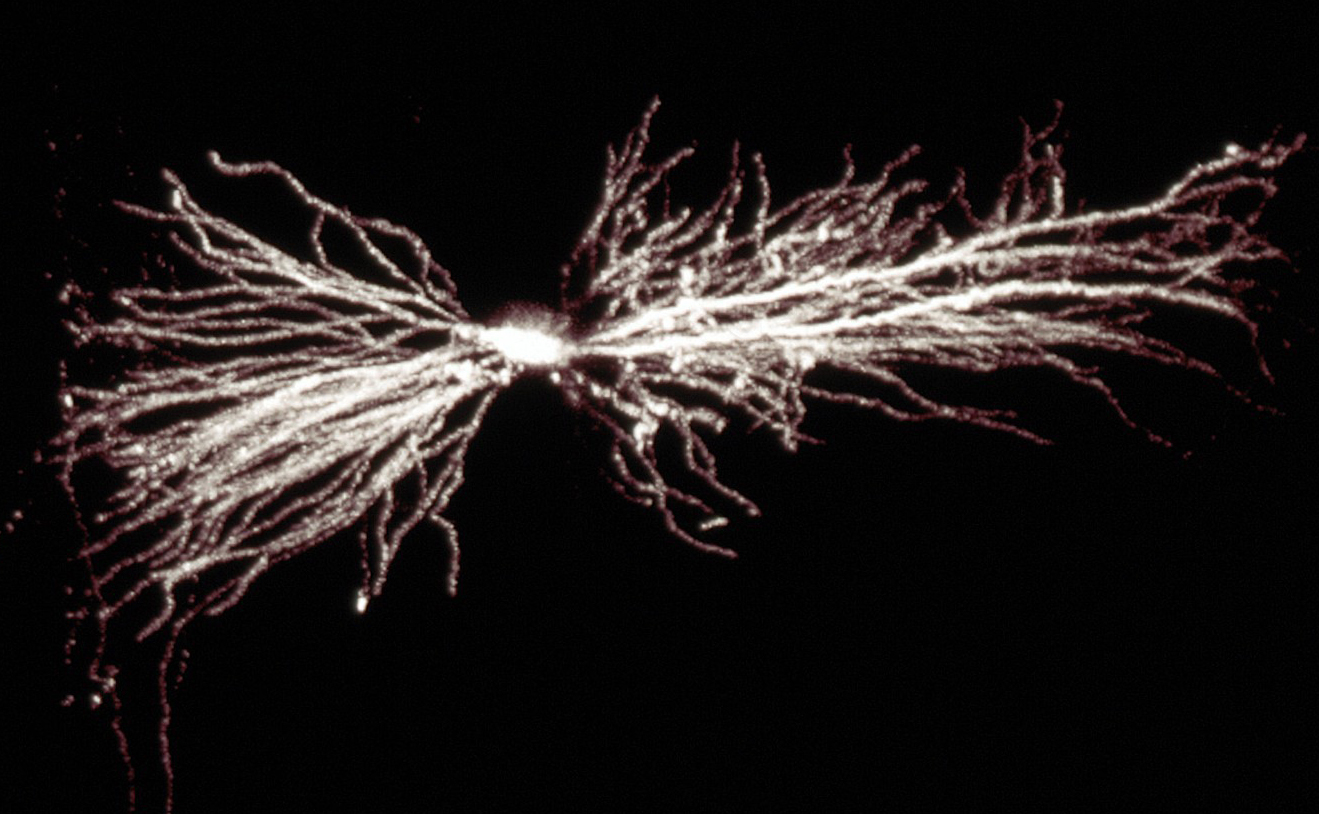 A hippocampal interneuron. Image: Biosciences Imaging Gp, Soton, Wellcome Trust via Creative Commons