An April 14, 2016 news item on phys.org describes a new 3D fabrication technique devised by Chinese scientists,
Nature is no doubt the world’s best biological engineer, whose simple, exquisite but powerful designs have inspired scientists and engineers to tackle the challenges of technologies for centuries. Scientists recently mimicked the surface structure of a moth’s eye, a unique structure with an antireflective property, to develop a highly light-absorbent graphene material. This is breakthrough [sic] in solar cell technology. Rice leaves and butterfly wings also have unique self-cleaning surface characteristics, which inspire scientists to develop novel materials resistant to biofouling. The bio-inspired periodic multi-scale structures, called hierarchical structures, have recently caught broad attention among scientists in various applications such as solar cells, Light-emitting diodes (LEDs), biomaterials and anti-bacterial surfaces.
An April 14, 2016 Optical Society of American news release (also on EurekAlert), which originated the news item, provides more detail,
Although a number of techniques for fabricating bio-inspired hierarchical structures already exist, most conventional methods either involve complicated processes or are highly time-consuming and low cost-efficiency for industrial applications. Now, a team of researchers from Changchun University of Science and Technology, China, have developed a novel method for the rapid and maskless fabrication of bio-inspired hierarchical structures, using a technique called laser interference lithography.
Specifically, the researchers use the interference pattern of three-and four-beam lasers to fabricate ordered multi-scale surface structures on silicon substrates, with the pattern of hierarchical structures controllable by adjusting the parameters of incident light. In accordance with the theoretical and computer analysis, the researchers have experimentally demonstrated the novel technique’s potential in large-area, low-cost and high-volume 3D fabrication of micro and nanostructures. …
“We presented a flexible and direct method for fabricating ordered multi-scale 3D structures using three- and four-beam interference lithography,” said Zuobin Wang, the primary author and a professor of International Research Centre for Nano Handling and Manufacturing of China at the Changchun University of Science and Technology, China. “Compared with other patterning technologies, our method is simple and efficient in terms of obtaining bio-inspired hierarchical structures.”
Wang mentioned that for certain complicated surface structures, conventional techniques such as electron beam lithography may take several hours or a day to fabricate the pattern, while the laser interference approach only takes several minutes to generate the structure, which makes the technique suitable for high-volume industrial production.
“Laser interference lithography is a maskless patterning technique that uses the interference patterns generated from two or several coherent laser beams to fabricate micro and nanometer periodic patterns over large areas,” Wang said. Different from conventional patterning techniques like electron beam lithography, the laser interference technique enables fabricating the entire substrate surface with one single exposure or one-step lithography.
For example, in Wang’s experiment, the one-dimension multi-scale structure, that is, one-dimension oriented arrangement with the sinusoidal grooves covered with periodic line-like structures was fabricated by exposing the silicon substrate to three or four interfered beams for one time. The resultant surface pattern, though arranged in one direction, has three-dimension spatial structure. To obtain more complicated structures such as two-dimension oriented multi-scale structures, the researchers simply rotated the substrate by 90 degrees in the plane and applied second laser exposure to the surface.
“Laser interference lithography is capable of fabricating homogeneous micro and nanometer structured patterns over areas more than one square meter, which is either impossible or highly time or cost consuming for conventional techniques,” Wang said. These features make laser interference lithography superior to other techniques in terms of efficiency and high-volume production.
According to Wang, their experimental process is simple: a high power laser beam was split into three or four equal beams, which then were directed by mirrors to generate interference patterns to fabricate the surface structures. The laser parameters such as incident angle and azimuthal angle of each beam were adjusted by beam splitters and mirror positions. Other optical devices such as quarter-wave plates and polarizers were used to select the polarization mode and control the energy of laser beams.
“The laser beam parameters are selected according to the desired surface structure and corresponding interference energy distribution calculated from theoretical simulation. In other words, the shapes or patterns of hierarchical structures in our method are controllable by adjusting the parameters of each incident beams,” Wang noted.
According to Wang, the proposed technique could be used to fabricate optical or medical devices such as solar cells, antireflective coatings, self-cleaning and antibacterial surfaces and long-life artificial hip joints.
The researchers’ next step is to develop functional surface structures with controllable wettability, adhesion and reflectivity properties for optical, medical and mechanical applications.
Here’s a link to and a citation for the paper,
Bio-inspired hierarchical patterning of silicon by laser interference lithography by Yaowei Hu, Zuobin Wang, Zhankun Weng, Miao Yu, and Dapeng Wang. Applied Optics Vol. 55, Issue 12, pp. 3226-3232 (2016) doi: 10.1364/AO.55.003226
I believe this paper is behind a paywall.
The researchers have provided this image as an illustration of their concept,
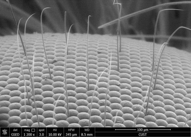
Caption: This is a Scanning Electron Microscope (SEM) image of a moth eye. Credit: Zuobin Wang/Changchun University of Science and Technology, China

