Tag Archives: optics

Outer space telescopes made of micro- and nanoparticles (smart dust)

Scientists at Rochester Institute of Technology (RIT is located in New York state) are working on a project that would see ‘smart dust’ used as a telescope in outer space. From a Dec. 1, 2014 news item on phys.org,

Telescope lenses someday might come in aerosol cans. Scientists at Rochester Institute of Technology and the NASA [ National Aeronautics and Space Administration] Jet Propulsion Laboratory are exploring a new type of space telescope with an aperture made of swarms of particles released from a canister and controlled by a laser.

These floating lenses would be larger, cheaper and lighter than apertures on conventional space-based imaging systems like NASA’s Hubble and James Webb space telescopes, said Grover Swartzlander, associate professor at RIT’s Chester F. Carlson Center for Imaging Science and Fellow of the Optical Society of America. Swartzlander is a co-investigator on the Jet Propulsion team led by Marco Quadrelli.

A Dec. 1, 2014 RIT news release by Susan Gawlowicz, which originated the news item, describes the NASA project and provides more details about the technology,

NASA’s Innovative Advanced Concepts Program is funding the second phase of the “orbiting rainbows” project that attempts to combine space optics and “smart dust,” or autonomous robotic system technology. The smart dust is made of a photo-polymer, or a light-sensitive plastic, covered with a metallic coating.

“Our motivation is to make a very large aperture telescope in space and that’s typically very expensive and difficult to do,” Swartzlander said. “You don’t have to have one continuous mass telescope in order to do astronomy—it can be distributed over a wide distance. Our proposed concept could be a very cheap, easy way to achieve large coverage, something you couldn’t do with the James Webb-type of approach.”

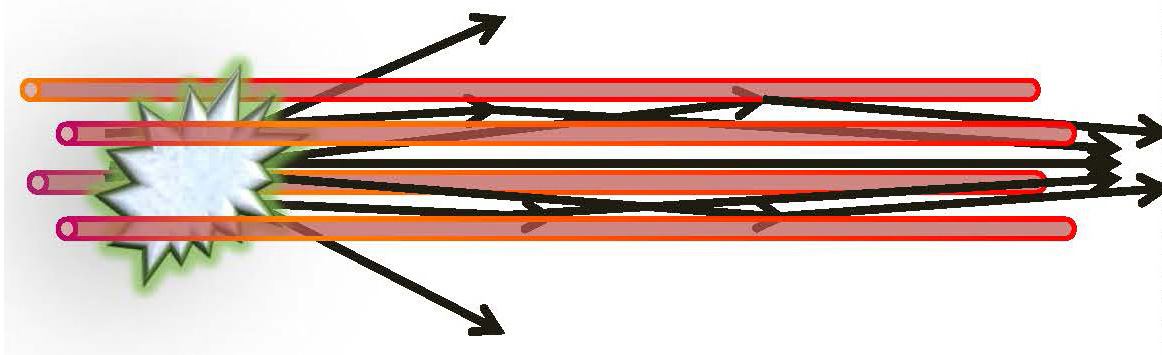
An adaptive optical imaging sensor comprised of tiny floating mirrors could support large-scale NASA missions and lead to new technology in astrophysical imaging and remote sensing.

Swarms of smart dust forming single or multiple lenses could grow to reach tens of meters to thousands of kilometers in diameter. According to Swartzlander, the unprecedented resolution and detail might be great enough to spot clouds on exoplanets, or planets beyond our solar system.

“This is really next generation,” Swartzlander said. “It’s 20, 30 years out. We’re at the very first step.”

Previous scientists have envisioned orbiting apertures but not the control mechanism. This new concept relies upon Swartzlander’s expertise in the use of light, or photons, to manipulate micro- or nano-particles like smart dust. He developed and patented the techniques known as “optical lift,” in which light from a laser produces radiation pressure that controls the position and orientation of small objects.

In this application, radiation pressure positions the smart dust in a coherent pattern oriented toward an astronomical object. The reflective particles form a lens and channel light to a sensor, or a large array of detectors, on a satellite. Controlling the smart dust to reflect enough light to the sensor to make it work will be a technological hurdle, Swartzlander said.

Two RIT graduate students on Swartzlander’s team are working on different aspects of the project. Alexandra Artusio-Glimpse, a doctoral student in imaging science, is designing experiments in low-gravity environments to explore techniques for controlling swarms of particle and to determine the merits of using a single or multiple beams of light.

Swartzlander expects the telescope will produce speckled and grainy images. Xiaopeng Peng, a doctoral student in imaging science, is developing software algorithms for extracting information from the blurred image the sensor captures. The laser that will shape the smart dust into a lens also will measure the optical distortion caused by the imaging system. Peng will use this information to develop advanced image processing techniques to reverse the distortion and recover detailed images.

“Our goal at this point is to marry advanced computational photography with radiation-pressure control techniques to achieve a rough image,” Swartzlander said. “Then we can establish a roadmap for improving both the algorithms and the control system to achieve ‘out of this world’ images.”

You can find out more about NASA’s Orbiting Rainbows project here.

I just mentioned rainbows and optics with regard to Robert Grosseteste, a 13th century cleric who ‘unwove’ rainbows, in a Dec. 1, 2014 posting (scroll down about 60% of the way).

December 2014 issue of the Nano Bite (from the Nanoscale Informal Science Education Network) features last day (Dec. 1, 2014) to apply for NanoDays 2015 physical kit and a bit about a medieval cleric who* ‘unwove’ light

Depending on your timezone, there are still a few hours left to submit an online application for a NanoDays 2015 physical kit. From a Sept. 15, 2014 posting by Catherine McCarthy for NISENet (Nanoscale Informal Science Education Network),

Apply now for a NanoDays 2015 physical kit!
NanoDays 2015 will be held from March 28 through April 5, 2015. NanoDays is a week of community-based educational outreach events to raise public awareness of nanoscale science, technology and engineering throughout the United States. NanoDays kits are currently in production and will be ready for distribution in early 2015. We invite you to fill out an online application for a physical kit containing all of the materials and resources you need to start planning your community events; applications are due December 1, 2014.


We’re in Year 10 of funding for NISE Net, what’s going to happen to NanoDays?

This is the final NanoDays physical kit that will be funded through the current NISE Net award. Beyond 2015, we encourage you to continue to host NanoDays and strengthen local partnerships by using this kit (and any previous kits you have). We’ve set dates for the next five years to promote national participation in NanoDays in the years to come.

Future NanoDays will be held:

  • 2016: March 26-April 3
  • 2017: March 25-April 2
  • 2018: March 31-April 8
  • 2019: March 30-April 7
  • 2020: March 28-April 5

The NISE Network leadership is seeking opportunities to continue NanoDays after 2015, so stay tuned for further information!

Who can participate in NanoDays?
NanoDays kits are intended for use in public events; most host organizations are informal science education institutions and public outreach programs of nanoscience research centers. We invite you and your organization to participate in NanoDays 2015, whether or not you have previous experience with nano-related public outreach activities.

For anyone unfamiliar with the NanoDays programs, the post goes on to provide more details.

Here’s more about the upcoming International Year of Light (IYL)  mentioned in my Nov. 7, 2014 post,

What’s Nano about Light?
The United Nations has declared that 2015 is the International Year of Light (IYL) and light-based technologies. This global initiative helps to highlight for the public the importance of light and optical technologies in ones’ everyday life and it’s role in the development of society and the future. Endorsed by the International Council of Science, the International Year of Light 2015 has more than 100 partners from more than 85 countries!

Are you looking for ways to get involved?

There’s this tidbit about a special event featuring the University of Vermont physics department, light, and a local watershed (from the newsletter),

A Bi-Polar Affair Captivates Visitors with EnLIGHTening Nanoscale Science

By Luke Donforth, The University of Vermont

The University of Vermont (UVM) Physics Department and ECHO Lake Aquarium and Science Center have a long collaborative relationship, through which the NISE Network has provided an excellent framework to help strengthen and deepen. Although an institution of formal learning, UVM values and contributes to informal education in the surrounding community.

Recently, the UVM Physics Department and ECHO received a NISE Net mini-grant to develop a daylong event outside the purview of NanoDays. ECHO focuses on the Lake Champlain watershed, and the Physics Department wanted to show how basic science is a useful tool for investigating, understanding, and caring for the lake and world around us. Light, and specifically polarization, gave us a unifying theme to bring a number of activities and concepts to ECHO. Visible light, something most museum visitors have experience with, has wavelengths in the hundreds of nanometers. This provides a comfortable entry point to familiarize visitors with “nano,” and from there we can highlight how interacting with light at the length scale of its wavelength allows us to investigate both light and the world around us.

….

Polarization, the orientation of components of light, provides a tool with uses ranging from telling the time of day to monitoring invasive species in Lake Champlain. As an example of the later, Professor J. Ellen Marsden (an ichthyologist with UVM’s Rubenstein School of Environment and Natural Resources and long-time ECHO collaborator) supplied samples of larval zebra mussels from Lake Champlain. Zebra mussels, an invasive species actively monitored in the lake, are more easily distinguished and detected earlier with the thoughtful application polarized light.

We’re going to be hearing a lot more about light as we gear up for 2015. Meanwhile, you can read the entire December 2014 issue of the Nano Bite here.

In keeping with my previous comment, there’s this bit about a medieval cleric who helped us to understand light and optics. From a Nov. 27, 2014 posting by Michael Brooks, on the Guardian science blog, concerning his recent participation in a Festival of Humanities event held at the medieval Durham Cathedral,

Robert Grosseteste was a medieval pioneer of science. And, despite having died in 1253, the good bishop is up for an award on Thursday night [Nov. 27, 2014]. The shortlist for the Times Higher Education’s 2014 Research Project of the Year includes the researchers from Durham University who laid on last week’s activities in the cathedral’s Chapter House and Deanery, and they openly describe Grosseteste as one of their collaborators.

They made this clear in a paper they published in the prestigious journal Nature Physics in July. The scientists are re-examining Grosseteste’s work, and finding he made contributions to the field of optics that have yet to be assimilated into the canon of science. So they’ve come on board to help complete the record.

Grosseteste’s insight into the physics of rainbows has, for instance, enabled the researchers in the Ordered Universe collaboration to create a new co-ordinate system for colour. Anyone who has tried to calibrate a computer monitor knows that we now talk in terms of hue (a particular ratio of red, green and blue), saturation and brightness. Examination of Grosseteste’s writings has inspired an equally valid rainbow-based colour system.

It is based on the angle through which sunlight is scattered by the water drops, the “purity” of the medium – related to the size of the water drops – and the distance of the sun above the horizon. Grosseteste’s three-dimensional scheme outlines what Durham physicist Tom McLeish calls “the space of all possible rainbows”.

Here’s an image of a rainbow over Durham Cathedral,

 Rainbow over Durham Cathedral by StephieBee [downloaded from https://www.flickr.com/photos/visitengland/galleries/72157625178514241/]


Rainbow over Durham Cathedral
by StephieBee [downloaded from https://www.flickr.com/photos/visitengland/galleries/72157625178514241/]

Here’s where you can find more of StephieBee‘s work.

Sadly, GrosseTeste did not win top prize but I’m sure if he were still around, he’d say something like, “It was an honour to be nominated and I thank God.” As for the Festival of Humanities (Being Human), there’s more here about its 2014 inaugural year.

*Changed ‘on’ to ‘who’ in headline on Dec. 2, 2014.

Ethereal optical cables

It’s a gobsmacking idea but here’s what scientist Howard Milchberg wants to accomplish (from a July 22, 2014 University of Maryland (UMD) news release (also on EurekAlert) [written by Brian Doctrow]),

Imagine being able to instantaneously run an optical cable or fiber to any point on earth, or even into space. That’s what Howard Milchberg, professor of physics and electrical and computer engineering at the University of Maryland, wants to do.

In a paper published today in the July 2014 issue of the journal Optica, Milchberg and his lab report using an “air waveguide” to enhance light signals collected from distant sources. These air waveguides could have many applications, including long-range laser communications, detecting pollution in the atmosphere, making high-resolution topographic maps and laser weapons.

Here’s an image illustrating the first step to achieving ‘ethereal cables’, an air waveguide,

Caption: This is an illustration of an air waveguide. The filaments leave 'holes' in the air (red rods) that reflect light. Light (arrows) passing between these holes stays focused and intense. Credit: Howard Milchberg

Caption: This is an illustration of an air waveguide. The filaments leave ‘holes’ in the air (red rods) that reflect light. Light (arrows) passing between these holes stays focused and intense.
Credit: Howard Milchberg

Here’s more about precursor research into creating air waveguides, from the news release,

Milchberg showed previously that these filaments heat up the air as they pass through, causing the air to expand and leaving behind a “hole” of low-density air in their wake. This hole has a lower refractive index than the air around it. While the filament itself is very short lived (less than one-trillionth of a second [less than a picosecond]), it takes a billion times longer for the hole to appear. It’s “like getting a slap to your face and then waiting, and then your face moves,” according to Milchberg, who also has an appointment in the Institute for Research in Electronics and Applied Physics at UMD.

On Feb. 26, 2014, Milchberg and his lab reported in the journal Physical Review X that if four filaments were fired in a square arrangement, the resulting holes formed the low-density wall needed for a waveguide. When a more powerful beam was fired between these holes, the second beam lost hardly any energy when tested over a range of about a meter. Importantly, the “pipe” produced by the filaments lasted for a few milliseconds, a million times longer than the laser pulse itself. For many laser applications, Milchberg says, “milliseconds [thousandths of a second] is infinity.”

The latest work brings Milchberg a step closer to using air waveguides as cables for lasers (from the news release),

Because light loses intensity with distance, the range over which such tasks can be done is limited. Even lasers, which produce highly directed beams, lose focus due to their natural spreading, or worse, due to interactions with gases in the air. Fiber-optic cables can trap light beams and guide them like a pipe, preventing loss of intensity or focus.

Typical fibers consist of a transparent glass core surrounded by a cladding material with a lower index of refraction. When light tries to leave the core, it gets reflected back inward. But solid optical fibers can only handle so much power, and they need physical support that may not be available where the cables need to go, such as the upper atmosphere. Now, Milchberg’s team has found a way to make air behave like an optical fiber, guiding light beams over long distances without loss of power.

Milchberg’s air waveguides consist of a “wall” of low-density air surrounding a core of higher density air. The wall has a lower refractive index than the core—just like an optical fiber. In the Optica paper, Milchberg, physics graduate students Eric Rosenthal and Nihal Jhajj, and associate research scientist Jared Wahlstrand, broke down the air with a laser to create a spark. An air waveguide conducted light from the spark to a detector about a meter away. The researchers collected a strong enough signal to analyze the chemical composition of the air that produced the spark.

The signal was 1.5 times stronger than a signal obtained without the waveguide. That may not seem like much, but over distances that are 100 times longer, where an unguided signal would be severely weakened, the signal enhancement could be much greater.

Milchberg creates his air waveguides using very short, very powerful laser pulses. A sufficiently powerful laser pulse in the air collapses into a narrow beam, called a filament. This happens because the laser light increases the refractive index of the air in the center of the beam, as if the pulse is carrying its own lens with it.

Because the waveguides are so long-lived, Milchberg believes that a single waveguide could be used to send out a laser and collect a signal. “It’s like you could just take a physical optical fiber and unreel it at the speed of light, put it next to this thing that you want to measure remotely, and then have the signal come all the way back to where you are,” says Milchberg.

First, though, he needs to show that these waveguides can be used over much longer distances—50 meters at least. If that works, it opens up a world of possibilities. Air waveguides could be used to conduct chemical analyses of places like the upper atmosphere or nuclear reactors, where it’s difficult to get instruments close to what’s being studied. The waveguides could also be used for LIDAR, a variation on radar that uses laser light instead of radio waves to make high-resolution topographic maps.

Here are links to and citations for both papers from Milchberg’s research team,

Demonstration of Long-Lived High-Power Optical Waveguides in Air by N. Jhajj, E. W. Rosenthal, R. Birnbaum, J. K. Wahlstrand, and H. M. Milchberg. Physical Review X: http://dx.doi.org/10.1103/PhysRevX.4.011027 Published Feb. 26, 2014

Collection of remote optical signals by air waveguides by E. W. Rosenthal, N. Jhajj, J. K. Wahlstrand, and H. M. Milchberg. Optica, Vol. 1, Issue 1, pp. 5-9 (July 2014) http://dx.doi.org/10.1364/OPTICA.1.000005

Both papers are open access.

Atlantic Canada’s Lamda Guard signs deal to test nanocomposite windshield film with Airbus

This story comes from Nova Scotia although you wouldn’t know it if you’d only read the June 5, 2014 news item on Azonano,

Lamda Guard, a company based in Atlantic Canada, has signed an agreement with leading aircraft manufacturer Airbus to test a breakthrough innovation designed to deflect unwanted bright light or laser sources from impacting jetliner flight paths, and causing pilot disorientation or injury.

A June 4, 2014 news release (either from Lamda Guard.com or MTI [metamaterial.com]; Note: More about the multiple webspaces later] and there’s a PDF version here), which originated the news item, provides a little more information about the technology and the perspectives from various stakeholders

Lamda Guard’s innovative thin films utilize metamaterial technology on cockpit windscreens to selectively block and control light coming from any angle even at the highest power levels. “Today marks a milestone in optical applications of nano-composites,” said George Palikaras, President and CEO of Lamda Guard. “Through our collaboration with Airbus we are working to introduce our metamaterial technology, for the first time, as a solution to laser interference in the aviation industry.” The announcement today comes within weeks of the release of an FBI [US Federal Bureau of Investigation] report citing 3,960 aircraft laser strikes in the US in 2013 according to the Federal Aviation Authority (FAA).

Senior Vice President of Innovation Yann Barbaux stated: “At Airbus, we are always on the lookout for new ideas coming from innovative SMEs [small to medium enterprises], such as Lamda Guard. We are very pleased to explore together the potential application of this solution to our aircraft, for the benefit of our customers.”

Over the past year Lamda Guard has been working with the research community at the University of Moncton and the University of New Brunswick, as well as stakeholders, investors and funders to highlight the benefits of nano-composites. The Atlantic Canada Opportunities Agency (ACOA) in particular has played an important role in Lamda Guard’s research and development efforts. In 2012, ACOA assisted Lamda Guard with technology commercialization and recently upgraded its contribution to $500,000 to further assist the company in developing and manufacturing its products for the aviation industry.

The Lamda Guard Airbus partnership marks the first time an optical metamaterial nano-composite has been applied on a large-scale surface.

I tried to find more information about the technology and tracked down this tiny bit, from the What are MetaMaterials? webpage on the MTI website,

A metamaterial typically consists of a multitude of structured unit cells that are comprised of multiple individual elements, which are referred to as meta-atoms. The individual elements are assembled from conventional microscopic materials such as metals and/or plastics, which are arranged in periodic patterns.

MTI’s precisely designed structures are developed with proprietary algorithms, producing a new generation of optical products that are built in state-of-the-art thin film nano-fabrication labs. MTI’s proprietary software accurately predicts the desired design pattern to generate a unique material that meets customer specifications. MTI’s sleek designs mean manufacturers can reduce their cost of materials significantly while increasing performance, e.g. by increasing the light output of an LED bulb or increasing the absorption of light in a solar panel.

Multiple webspaces and presences

While Lamda Guard has a .com presence, you will find yourself on the metamaterial.com website in the Lamda Guard webspace (I suppose you could also call it a subsite) once you start clicking for more information.  In fact, MTI owns three Lamda companies as per this description from the Our Company webpage on the MTI (metamaterial.com) website (Note: Links have been removed),

MTI is an advanced materials and systems engineering company developing and commercializing innovative optical solutions. The company’s core team has over 200 years of combined experience at the forefront of the design and implementation of metamaterials, making MTI a pioneer in bridging the gap between the theoretical and the possible.

MTI specializes in metamaterials, nanotechnology, theoretical and computational electromagnetics. The company’s in-house expertise enables the rapid development of a wide array of metamaterial applications, covering a diverse range of markets.

MTI’s technologies are adaptable and can be custom-designed to suit an industry manufacturer’s specifications allowing for scalability and rapid prototyping with minimum overheads. MTI provides access to world class nano-composite research and development, including specialty, as well as customized, products and licensing of its proprietary solutions to customers ranging from government to private companies.

MTI has three wholly owned subsidiaries:

Lamda Guard Inc. which develops advanced filters to block out selected parts of the light spectrum, protecting the eyes from lasers or other sources of hazardous light.

Lamda Solar Inc. products increase the efficiency of solar panel cells by absorbing more light.

Lamda Lux Inc. technology increases the delivered lumens and reduces the cost of thermal management of LED lighting.

Interestingly, the Lamda Guard Management team‘s (in the Lamda Guard webspace) Chief Science Officer, Dr. Themos Kallos, and Chief Intellectual Property Officer, Dr. Quinton Fivelman, both appear to reside in the UK (assuming I looked at the correct LinkedIn profiles).  Coincidentally, MTI’s contact page lists the company’s headquarters as being in Nova Scotia but Sales, Research and Development would seem to be located in the UK.

Presumably, this company is maximizing its access to government grants and tax incentives in both the UK and Canada. The deal with the Airbus suggests that this has been a successful strategy possibly leading to commercialized technology and, hopefully, jobs.

From Australia: a recipe for baking lenses

Here’s the recipe from an April 24, 2014 Optical Society news release on EurekAlert,

All that’s needed is an oven, a microscope glass slide and a common, gel-like silicone polymer called polydimethylsiloxane (PDMS). First, drop a small amount of PDMS onto the slide. Then bake it at 70 degrees Celsius to harden it, creating a base. Then, drop another dollop of PDMS onto the base and flip the slide over. Gravity pulls the new droplet down into a parabolic shape. Bake the droplet again to solidify the lens. More drops can then be added to hone the shape of the lens that also greatly increases the imaging quality of the lens. “It’s a low cost and easy lens-making recipe,” Lee [ Steve Lee from the Research School of Engineering at Australian National University] says.

I’m still marveling over this image,

Caption: This photo shows a single droplet lens suspended on a fingertip. Credit: Stuart Hay. Courtesy: The Optical Society

Caption: This photo shows a single droplet lens suspended on a fingertip. Credit: Stuart Hay. Courtesy: The Optical Society

For anyone who doesn’t know much about producing lenses and why these baked droplets could improve lives, the Optical Society news release provides some insight,

A droplet of clear liquid can bend light, acting as a lens. Now, by exploiting this well-known phenomenon, researchers have developed a new process to create inexpensive high quality lenses that will cost less than a penny apiece.

Because they’re so inexpensive, the lenses can be used in a variety of applications, including tools to detect diseases in the field, scientific research in the lab and optical lenses and microscopes for education in classrooms.

“What I’m really excited about is that it opens up lens fabrication technology,” says Steve Lee from the Research School of Engineering at Australian National University (ANU) …

Many conventional lenses are made the same way lenses have been made since the days of Isaac Newton—by grinding and polishing a flat disk of glass into a particular curved shape. Others are made with more modern methods, such as pouring gel-like materials molds. But both approaches can be expensive and complex, Lee says. With the new method, the researchers harvest solid lenses of varying focal lengths by hanging and curing droplets of a gel-like material—a simple and inexpensive approach that avoids costly or complicated machinery.

“What I did was to systematically fine-tune the curvature that’s formed by a simple droplet with the help of gravity, and without any molds,” he explains.

Although people have long recognized that a droplet can act as a lens, no one tried to see how good a lens it could be. Now, the team has developed a process that pushes this concept to its limits, Lee says.

The researchers made lenses about a few millimeters thick with a magnification power of 160 times and a resolution of about 4 microns (millionths of a meter)—two times lower in optical resolution than many commercial microscopes, but more than three orders of magnitude lower in cost. “We’re quite surprised at the magnification enhancement using such a simple process,” he notes.

An April 24, 2014 Australian National University (ANU) news release on EurekAlert adds more details to the story,

The lenses are made by using the natural shape of liquid droplets.

“We put a droplet of polymer onto a microscope cover slip and then invert it. Then we let gravity do the work, to pull it into the perfect curvature,” Dr Lee said.

“By successively adding small amounts of fluid to the droplet, we discovered that we can reach a magnifying power of up to 160 times with an imaging resolution of four micrometers.”

The polymer, polydimethylsiloxane (PDMS), is the same as that used for contact lenses, and it won’t break or scratch.

“It would be perfect for the third world. All you need is a fine tipped tool, a cover slip, some polymer and an oven,” Dr Lee said.

The first droplet lens was made by accident. [emphasis mine]

I nearly threw them away. [emphasis mine] I happened to mention them to my colleague Tri Phan, and he got very excited,” Dr Lee said.

“So then I decided to try to find the optimum shape, to see how far I could go. When I saw the first images of yeast cells I was like, ‘Wow!'”

Dr Lee and his team worked with Dr Phan to design a lightweight 3D-printable frame to hold the lens, along with a couple of miniature LED lights for illumination, and a coin battery.

The technology taps into the current citizen science revolution [emphasis mine], which is rapidly transforming owners of smart phones into potential scientists. There are also exciting possibilities for remote medical diagnosis.

Dr Phan said the tiny microscope has a wide range of potential uses, particularly if coupled with the right smartphone apps.

“This is a whole new era of miniaturisation and portability – image analysis software could instantly transform most smartphones into sophisticated mobile laboratories,” Dr Phan said.

“I am most able to see the potential for this device in the practice of medicine, although I am sure specialists in other fields will immediately see its value for them.”

Dr Lee said the low-cost lens had already attracted interest from a German group interested in using disposable lenses for tele-dermatology.

“There are also possibilities for farmers,” he said. “They can photograph fungus or insects on their crops, upload the pictures to the internet where a specialist can identify if they are a problem or not.”

That Lee created his first droplet by accident and almost threw it away echoes many, many other science stories. In addition to that age old science story, I love the simplicity of the idea, the reference to Isaac Newton, and the inclusion of citizen science.

Here’s a link to and a citation for the paper,

Fabricating low cost and high performance elastomer lenses using hanging droplets by W. M. Lee, A. Upadhya, P. J. Reece, and Tri Giang Phan. Biomedical Optics Express, Vol. 5, Issue 5, pp. 1626-1635 (2014) http://dx.doi.org/10.1364/BOE.5.001626

This paper is open access.

I wish Lee and his team great success in making this technology available, assuming that it lives up to its promise.

Taking photos and videos in near darkness

Who hasn’t found wanted to take a picture in a situation where there’s very little light? It seems scientists at SUNY (State University of New York) College of Nanoscale Science and Engineering (CNSE) have found a way to solve the problem. From a Jan. 30, 2014 news item on Azonano,

When the lights went out at the big game, fans and film crews struggled to take a decent picture in the darkness. Those same folks will be cheering the latest research by a team of SUNY College of Nanoscale Science and Engineering (CNSE) scientists, which makes brilliant video and pictures possible even if the lights go out.

Dark and blurry low light photos could soon be a thing of the past, thanks to the development of game-changing ultrathin “nanosheets,” which could dramatically improve imaging technology used in everything from cell phone cameras, video cameras, solar cells, and even medical imaging equipment such as MRI machines.

As a result, this technology is perfectly suited for inclusion in a wide variety of everyday devices, including today’s smartphones, which are often used to take pictures, but suffer from limitations in low light environments. This research could allow even novice photographers to take sharper images, even in the midst of a blackout during the biggest game of the year.

A SUNYCNSE research profile titled: SUNY College of Nanoscale Science and Engineering Scientists Publish Game-Changing Semiconductor Nanosheets Research That Could Revolutionize Cameras in Low-Light Environments provides more technical details about the research,

Leading-edge research by a team of SUNY College of Nanoscale Science and Engineering (CNSE) scientists has been published in ACS Nano after the scientists evaluated ultrathin indium(III) selenide (In2Se3) nanosheets and discovered that their electrical resistance drops significantly when exposed to light. This effect, known as a photoconductive response, can be used to make a photodetector or light sensor, and because the two-dimensional nanosheets exhibited such a strong photoconductive response across a broad light spectrum and simultaneously resist chemical contamination, this research could lead to a revolution in extreme low-light, high-resolution imaging products and applications, such as consumer and professional cameras and video cameras, for example.

The team combined a variety of cutting-edge tools and methods, including scanning electron microscopy (SEM) to identify the nanosheets; atomic force microscopy (AFM) to measure their thickness; X-ray diffractometry (XRD) and selected area electron diffraction (SAED) combined with high-resolution images from transmission electron microscopy (TEM) to examine nano-layer details such as the crystallographic phase and morphology of the sample; and energy-dispersive X-ray spectrometry (EDS) and auger electron spectrometry (AES) to explore the sample’s homogeneity. As the photoconductive material’s properties were characterized, the CNSE research group found that the material is extremely resistant to contamination. Additionally, the team utilized a green LED to direct pulsed light at the nanosheets and found that they exhibited a reliable response to light and an excellent response time between 18 and 73 milliseconds, indicating that In2Se3 nanosheets could be a highly effective material for real-time imaging purposes.

The nanosheets were also tested for the ability to detect light and for light responsivity, or the ratio of generated photocurrent to incident light power. The researchers noted that the photoconductive response of the nanosheets, which had a thickness of 3.9 nanometers, was demonstrably higher than other 2D photoresistors across a broad light spectrum, including Ultraviolet, visible light, and infrared, making them suitable for use in a wide-range of imaging devices.

Here’s a link to and a citation for the paper,

Extraordinary Photoresponse in Two-Dimensional In2Se3 Nanosheets by Robin B. Jacobs-Gedrim, Mariyappan Shanmugam, Nikhil Jain, Christopher A. Durcan, Michael T. Murphy, Thomas M. Murray, Richard J. Matyi, Richard L. Moore, II, and Bin Yu.  ACS Nano (2014), vol. 8, no. 1, pp. 514-21

This is a PDF of the document and is being made available by the researchers and their institution.

New hydrogels make greater elasticity in tissue engineering possible

A team from Harvard University have developed a technique for creating hydrogels that could be used effective in tissue engineering projects. From the Sept. 5, 2012 news release on EurekAlert,

A team of experts in mechanics, materials science, and tissue engineering at Harvard have created an extremely stretchy and tough gel that may pave the way to replacing damaged cartilage in human joints.

Called a hydrogel, because its main ingredient is water, the new material is a hybrid of two weak gels that combine to create something much stronger. Not only can this new gel stretch to 21 times its original length, but it is also exceptionally tough, self-healing, and biocompatible—a valuable collection of attributes that opens up new opportunities in medicine and tissue engineering.

Here’s an image of the hydrogel provided by the researchers,

The researchers pinned both ends of the new gel in clamps and stretched it to 21 times its initial length before it broke. Credit: Photo courtesy of Jeong-Yun Sun

The Sept. 5, 2012 news item on ScienceDaily has some comments from the researcher,

“Conventional hydrogels are very weak and brittle — imagine a spoon breaking through jelly,” explains lead author Jeong-Yun Sun, a postdoctoral fellow at the Harvard School of Engineering and Applied Sciences (SEAS). “But because they are water-based and biocompatible, people would like to use them for some very challenging applications like artificial cartilage or spinal disks. For a gel to work in those settings, it has to be able to stretch and expand under compression and tension without breaking.”

To create the tough new hydrogel, they combined two common polymers. The primary component is polyacrylamide, known for its use in soft contact lenses and as the electrophoresis gel that separates DNA fragments in biology labs; the second component is alginate, a seaweed extract that is frequently used to thicken food.

Separately, these gels are both quite weak — alginate, for instance, can stretch to only 1.2 times its length before it breaks. Combined in an 8:1 ratio, however, the two polymers form a complex network of crosslinked chains that reinforce one another. The chemical structure of this network allows the molecules to pull apart very slightly over a large area instead of allowing the gel to crack.

The alginate portion of the gel consists of polymer chains that form weak ionic bonds with one another, capturing calcium ions (added to the water) in the process. When the gel is stretched, some of these bonds between chains break — or “unzip,” as the researchers put it — releasing the calcium. As a result, the gel expands slightly, but the polymer chains themselves remain intact. Meanwhile, the polyacrylamide chains form a grid-like structure that bonds covalently (very tightly) with the alginate chains.

Therefore, if the gel acquires a tiny crack as it stretches, the polyacrylamide grid helps to spread the pulling force over a large area, tugging on the alginate’s ionic bonds and unzipping them here and there. The research team showed that even with a huge crack, a critically large hole, the hybrid gel can still stretch to 17 times its initial length.

Importantly, the new hydrogel is capable of maintaining its elasticity and toughness over multiple stretches.

Anyone can see that the ability to stretch, self-heal and stretch mimics the body’s own processes and that materials which can mimic those processes are very promising. From the news item on ScienceDaily,

Beyond artificial cartilage, the researchers suggest that the new hydrogel could be used in soft robotics, optics, artificial muscle, as a tough protective covering for wounds, or “any other place where we need hydrogels of high stretchability and high toughness.”

If you’re interested, there are still more details in the news release on EurekAlert or in the news item on ScienceDaily.

Transformation optics and RockSalt poetry

According to today’s (Oct. 17, 2008) issue of Science, there’s a new field called Transformation Optics. Vladimir M. Shalaev wrote the article which lays out an explanation referencing Einstein’s theory of general relativity where space and time are curved but applying the notion to curving light in arbitrary fashion. Shalaev also discusses some exciting applications including the invisibility cloaks that have been discussed in the blogosphere for the last while. The article titled “Transforming Light” is in the Perspectives section of the magazine. Note: It is behind a paywall. You can find more information about the article and proposed applications here.

The first anthology of BC poetry in 30 years, RockSalt, is being launched with readings from the anthology, which includes over 100 BC poets, on Oct. 23, 2008 at 7 pm at the Agro Cafe (1363 Railspur Alley) on Granville Island . The list of poets who’ll be reading selections on Thurs. (Oct. 23) includes: Heather Haley, Harold Rhenisch, Kate Braid, Mona Fertig, Kuldip Gill, etc.