Tag Archives: organic semiconductors

Pressure-cooking birch leaves to produce nanoscale carbon particles for organic semiconductors

By pressure cooking birch leaves picked on campus the scientists produced carbon particles that can be used as raw material for the production of organic semiconductors. Image: Mattias Pettersson

A November 28, 2023 news item on phys.org announces work on an organic semiconductor,

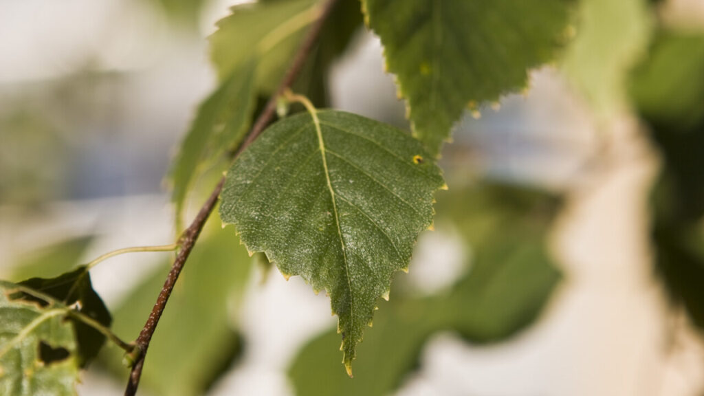
Today, petrochemical compounds and rare metals such as platinum and iridium are used to produce semiconductors for optoelectronics, such as organic LEDs for super-thin TV and mobile phone screens. Physicists at Umeå University in collaboration with researchers in Denmark and China, have discovered a more sustainable alternative. By pressure-cooking birch leaves picked on the Umeå University campus, they have produced a nanosized carbon particle with desired optical properties.

A January 28, 2023 Umeå University press release by Anna-Lena Lindskog, which originated the news item, provides more information about the research,

“The essence of our research is to harness nearby renewable resources for producing organic semiconductor materials” says Jia Wang, research fellow at the Department of Physics, Umeå University, and one of the authors of the study that has been published in the Green Chemistry.

Organic semiconductors are one of the most important functional materials in optoelectronic applications. One example is the organic light-emitting diodes, OLEDs, which enable ultra-thin and bright TV and mobile phone screens. Sharply increasing demand for this advanced technology is driving massive production of organic semiconductor materials.

Unfortunately, these semiconductors are currently produced mainly from petrochemical compounds and rare elements, obtained through environmentally harmful mining. Moreover, these materials often contain so-called ‘critical raw materials’ that are in short supply, such as Platinum, Indium and Phosphorus.

From a sustainability point of view, it would be ideal if we can use biomass from plants, animals and waste to produce organic semiconductor materials. These starting materials are renewable and abundantly available. Research fellow Jia Wang and her colleagues at the Department of Physics, together with international partners, have succeeded in producing such a bio-based semiconductor material.

Birch leaves in pressure cooker

The synthesis process is simple: they picked birch leaves on the Umeå campus and cooked them in a pressure cooker. That produced a kind of ‘carbon dots’ about two nanometers in size, which emit a narrow-band, deep red light when dissolved in ethanol. Some of the optical properties of these birch leaf carbon dots are comparable to commercial quantum dots currently used in semiconductor materials, but unlike them, they contain no heavy metals or critical raw materials.

”It is important to note that our method is not limited to birch leaves” explains Jia Wang. “We tested different plant leaves with the same pressure cooking method, and all of them produced similar red-emitting carbon dots. This versatility suggests that the transformation process can be used in different locations.”

Using the carbon dots in a light-emitting electrochemical cell device, the researchers were able to show that the brightness generated was 100 cd/m2, which is comparable to the light intensity from a computer screen.

“It is important to note that our method is not limited to birch leaves.”

”This result shows that it is possible to transition from depleting petroleum compounds to regenerating biomass as a raw material for organic semiconductors” says Jia Wang.

She emphasises the broader potential of carbon dots beyond just light-emitting devices.

“Carbon dots are promising across various applications, from bioimaging and sensing to anti-counterfeiting. We’re open to collaborations and eager to explore more exciting uses for these emissive and sustainable carbon dots” says Jia Wang.

Here’s a link to and a citation for the paper,

Fluorescent carbon dots from birch leaves for sustainable electroluminescent devices by Shi Tang, Yongfeng Liu, Henry Opoku, Märta Gregorsson, Peijuan Zhang, Etienne Auroux, Dongfeng Dang, Anja-Verena Mudring, Thomas Wågberg, Ludvig Edman, and Jia Wang. Green Chem., 2023, 25, 9884-9895 DOI: https://doi.org/10.1039/D3GC03827K First published: 01 Nov 2023

This paper is open access.

A different type of ‘smart’ window with a new solar cell technology

I always like a ‘smart’ window story. Given my issues with summer (I don’t like the heat), anything which promises to help reduce the heat in my home at that time of year, has my vote. Unfortunately, solutions don’t seem to have made a serious impact on the marketplace. Nonetheless, there’s always hope and perhaps this development at Princeton University will be the one to break through the impasse. From a June 30, 2017 news item on ScienceDaily,

Smart windows equipped with controllable glazing can augment lighting, cooling and heating systems by varying their tint, saving up to 40 percent in an average building’s energy costs.

These smart windows require power for operation, so they are relatively complicated to install in existing buildings. But by applying a new solar cell technology, researchers at Princeton University have developed a different type of smart window: a self-powered version that promises to be inexpensive and easy to apply to existing windows. This system features solar cells that selectively absorb near-ultraviolet (near-UV) light, so the new windows are completely self-powered.

A June 30, 2017 Princeton University news release, which originated the news item, expands on the theme,

“Sunlight is a mixture of electromagnetic radiation made up of near-UV rays, visible light, and infrared energy, or heat,” said Yueh-Lin (Lynn) Loo, director of the Andlinger Center for Energy and the Environment, and the Theodora D. ’78 and William H. Walton III ’74 Professor in Engineering. “We wanted the smart window to dynamically control the amount of natural light and heat that can come inside, saving on energy cost and making the space more comfortable.”

The smart window controls the transmission of visible light and infrared heat into the building, while the new type of solar cell uses near-UV light to power the system.

“This new technology is actually smart management of the entire spectrum of sunlight,” said Loo, who is a professor of chemical and biological engineering. Loo is one of the authors of a paper, published June 30, that describes this technology, which was developed in her lab.

Because near-UV light is invisible to the human eye, the researchers set out to harness it for the electrical energy needed to activate the tinting technology.

“Using near-UV light to power these windows means that the solar cells can be transparent and occupy the same footprint of the window without competing for the same spectral range or imposing aesthetic and design constraints,” Loo added. “Typical solar cells made of silicon are black because they absorb all visible light and some infrared heat – so those would be unsuitable for this application.”

In the paper published in Nature Energy, the researchers described how they used organic semiconductors – contorted hexabenzocoronene (cHBC) derivatives – for constructing the solar cells. The researchers chose the material because its chemical structure could be modified to absorb a narrow range of wavelengths – in this case, near-UV light. To construct the solar cell, the semiconductor molecules are deposited as thin films on glass with the same production methods used by organic light-emitting diode manufacturers. When the solar cell is operational, sunlight excites the cHBC semiconductors to produce electricity.

At the same time, the researchers constructed a smart window consisting of electrochromic polymers, which control the tint, and can be operated solely using power produced by the solar cell. When near-UV light from the sun generates an electrical charge in the solar cell, the charge triggers a reaction in the electrochromic window, causing it to change from clear to dark blue. When darkened, the window can block more than 80 percent of light.

Nicholas Davy, a doctoral student in the chemical and biological engineering department and the paper’s lead author, said other researchers have already developed transparent solar cells, but those target infrared energy. However, infrared energy carries heat, so using it to generate electricity can conflict with a smart window’s function of controlling the flow of heat in or out of a building. Transparent near-UV solar cells, on the other hand, don’t generate as much power as the infrared version, but don’t impede the transmission of infrared radiation, so they complement the smart window’s task.

Davy said that the Princeton team’s aim is to create a flexible version of the solar-powered smart window system that can be applied to existing windows via lamination.

“Someone in their house or apartment could take these wireless smart window laminates – which could have a sticky backing that is peeled off – and install them on the interior of their windows,” said Davy. “Then you could control the sunlight passing into your home using an app on your phone, thereby instantly improving energy efficiency, comfort, and privacy.”

Joseph Berry, senior research scientist at the National Renewable Energy Laboratory, who studies solar cells but was not involved in the research, said the research project is interesting because the device scales well and targets a specific part of the solar spectrum.

“Integrating the solar cells into the smart windows makes them more attractive for retrofits and you don’t have to deal with wiring power,” said Berry. “And the voltage performance is quite good. The voltage they have been able to produce can drive electronic devices directly, which is technologically quite interesting.”

Davy and Loo have started a new company, called Andluca Technologies, based on the technology described in the paper, and are already exploring other applications for the transparent solar cells. They explained that the near-UV solar cell technology can also power internet-of-things sensors and other low-power consumer products.

“It does not generate enough power for a car, but it can provide auxiliary power for smaller devices, for example, a fan to cool the car while it’s parked in the hot sun,” Loo said.

Here’s a link to and a citation for the paper,

Pairing of near-ultraviolet solar cells with electrochromic windows for smart management of the solar spectrum by Nicholas C. Davy, Melda Sezen-Edmonds, Jia Gao, Xin Lin, Amy Liu, Nan Yao, Antoine Kahn, & Yueh-Lin Loo. Nature Energy 2, Article number: 17104 (2017 doi:10.1038/nenergy.2017.104 Published online: 30 June 2017

This paper is behind a paywall.

Here’s what a sample of the special glass looks like,

Graduate student Nicholas Davy holds a sample of the special window glass. (Photos by David Kelly Crow)

Developing cortical implants for future speech neural prostheses

I’m guessing that graphene will feature in these proposed cortical implants since the project leader is a member of the Graphene Flagship’s Biomedical Technologies Work Package. (For those who don’t know, the Graphene Flagship is one of two major funding initiatives each receiving funding of 1B Euros over 10 years from the European Commission as part of their FET [Future and Emerging Technologies)] Initiative.)  A Jan. 12, 2017 news item on Nanowerk announces the new project (Note: A link has been removed),

BrainCom is a FET Proactive project, funded by the European Commission with 8.35M€ [8.3 million Euros] for the next 5 years, holding its Kick-off meeting on January 12-13 at ICN2 (Catalan Institute of Nanoscience and Nanotechnology) and the UAB [ Universitat Autònoma de Barcelona]. This project, coordinated by ICREA [Catalan Institution for Research and Advanced Studies] Research Prof. Jose A. Garrido from ICN2, will permit significant advances in understanding of cortical speech networks and the development of speech rehabilitation solutions using innovative brain-computer interfaces.

A Jan. 12, 2017 ICN2 press release, which originated the news item expands on the theme (it is a bit repetitive),

More than 5 million people worldwide suffer annually from aphasia, an extremely invalidating condition in which patients lose the ability to comprehend and formulate language after brain damage or in the course of neurodegenerative disorders. Brain-computer interfaces (BCIs), enabled by forefront technologies and materials, are a promising approach to treat patients with aphasia. The principle of BCIs is to collect neural activity at its source and decode it by means of electrodes implanted directly in the brain. However, neurorehabilitation of higher cognitive functions such as language raises serious issues. The current challenge is to design neural implants that cover sufficiently large areas of the brain to allow for reliable decoding of detailed neuronal activity distributed in various brain regions that are key for language processing.

BrainCom is a FET Proactive project funded by the European Commission with 8.35M€ for the next 5 years. This interdisciplinary initiative involves 10 partners including technologists, engineers, biologists, clinicians, and ethics experts. They aim to develop a new generation of neuroprosthetic cortical devices enabling large-scale recordings and stimulation of cortical activity to study high level cognitive functions. Ultimately, the BraimCom project will seed a novel line of knowledge and technologies aimed at developing the future generation of speech neural prostheses. It will cover different levels of the value chain: from technology and engineering to basic and language neuroscience, and from preclinical research in animals to clinical studies in humans.

This recently funded project is coordinated by ICREA Prof. Jose A. Garrido, Group Leader of the Advanced Electronic Materials and Devices Group at the Institut Català de Nanociència i Nanotecnologia (Catalan Institute of Nanoscience and Nanotechnology – ICN2) and deputy leader of the Biomedical Technologies Work Package presented last year in Barcelona by the Graphene Flagship. The BrainCom Kick-Off meeting is held on January 12-13 at ICN2 and the Universitat Autònoma de Barcelona (UAB).

Recent developments show that it is possible to record cortical signals from a small region of the motor cortex and decode them to allow tetraplegic [also known as, quadriplegic] people to activate a robotic arm to perform everyday life actions. Brain-computer interfaces have also been successfully used to help tetraplegic patients unable to speak to communicate their thoughts by selecting letters on a computer screen using non-invasive electroencephalographic (EEG) recordings. The performance of such technologies can be dramatically increased using more detailed cortical neural information.

BrainCom project proposes a radically new electrocorticography technology taking advantage of unique mechanical and electrical properties of novel nanomaterials such as graphene, 2D materials and organic semiconductors.  The consortium members will fabricate ultra-flexible cortical and intracortical implants, which will be placed right on the surface of the brain, enabling high density recording and stimulation sites over a large area. This approach will allow the parallel stimulation and decoding of cortical activity with unprecedented spatial and temporal resolution.

These technologies will help to advance the basic understanding of cortical speech networks and to develop rehabilitation solutions to restore speech using innovative brain-computer paradigms. The technology innovations developed in the project will also find applications in the study of other high cognitive functions of the brain such as learning and memory, as well as other clinical applications such as epilepsy monitoring.

The BrainCom project Consortium members are:

  • Catalan Institute of Nanoscience and Nanotechnology (ICN2) – Spain (Coordinator)
  • Institute of Microelectronics of Barcelona (CNM-IMB-CSIC) – Spain
  • University Grenoble Alpes – France
  • ARMINES/ Ecole des Mines de St. Etienne – France
  • Centre Hospitalier Universitaire de Grenoble – France
  • Multichannel Systems – Germany
  • University of Geneva – Switzerland
  • University of Oxford – United Kingdom
  • Ludwig-Maximilians-Universität München – Germany
  • Wavestone – Luxembourg

There doesn’t seem to be a website for the project but there is a BrainCom webpage on the European Commission’s CORDIS (Community Research and Development Information Service) website.

University of Vermont and the ‘excitons’ of an electron superhighway

This story starts off with one of the current crazes, folding and bendable electronics, before heading off onto the ‘electron highway’. From a Sept. 14, 2015 news item on ScienceDaily (Note: Links have been removed),

TV screens that roll up. Roofing tiles that double as solar panels. Sun-powered cell phone chargers woven into the fabric of backpacks. A new generation of organic semiconductors may allow these kinds of flexible electronics to be manufactured at low cost, says University of Vermont physicist and materials scientist Madalina Furis.

But the basic science of how to get electrons to move quickly and easily in these organic materials remains murky.

To help, Furis and a team of UVM materials scientists have invented a new way to create what they are calling “an electron superhighway” in one of these materials — a low-cost blue dye called phthalocyanine — that promises to allow electrons to flow faster and farther in organic semiconductors.

A Sept. 14, 2015 University of Vermont news release (also on EurekAlert) by Joshua E. Brown, which originated the news item, describes the problem the researches were trying to solve and the solution they found,

Hills and potholes

Many of these types of flexible electronic devices will rely on thin films of organic materials that catch sunlight and convert the light into electric current using excited states in the material called “excitons.” Roughly speaking, an exciton is a displaced electron bound together with the hole it left behind. Increasing the distance these excitons can diffuse — before they reach a juncture where they’re broken apart to produce electrical current — is essential to improving the efficiency of organic semiconductors.

Using a new imaging technique, the UVM team was able to observe nanoscale defects and boundaries in the crystal grains in the thin films of phthalocyanine — roadblocks in the electron highway. “We have discovered that we have hills that electrons have to go over and potholes that they need to avoid,” Furis explains.

To find these defects, the UVM team — with support from the National Science Foundation — built a scanning laser microscope, “as big as a table” Furis says. The instrument combines a specialized form of linearly polarized light and photoluminescence to optically probe the molecular structure of the phthalocyanine crystals.

“Marrying these two techniques together is new; it’s never been reported anywhere,” says Lane Manning ’08 a doctoral student in Furis’ lab and co-author on the new study.

The new technique allows the scientists a deeper understanding of how the arrangement of molecules and the boundaries in the crystals influence the movement of excitons. It’s these boundaries that form a “barrier for exciton diffusion,” the team writes.

And then, with this enhanced view, “this energy barrier can be entirely eliminated,” the team writes. The trick: very carefully controlling how the thin films are deposited. Using a novel “pen-writing” technique with a hollow capillary, the team worked in the lab of UVM physics and materials science professor Randy Headrick to successfully form films with jumbo-sized crystal grains and “small angle boundaries.” Think of these as easy-on ramps onto a highway — instead of an awkward stop sign at the top of a hill — that allow excitons to move far and fast.

Better solar cells

Though the Nature Communications study focused on just one organic material, phthalocyanine, the new research provides a powerful way to explore many other types of organic materials, too — with particular promise for improved solar cells. A recent U.S. Department of Energy report identified one of the fundamental bottlenecks to improved solar power technologies as “determining the mechanisms by which the absorbed energy (exciton) migrates through the system prior to splitting into charges that are converted to electricity.”

The new UVM study — led by two of Furis’ students, Zhenwen Pan G’12, and Naveen Rawat G’15 — opens a window to view how increasing “long-range order” in the organic semiconductor films is a key mechanism that allows excitons to migrate farther. “The molecules are stacked like dishes in a dish rack,” Furis explains, “these stacked molecules — this dish rack — is the electron superhighway.”

Though excitons are neutrally charged — and can’t be pushed by voltage like the electrons flowing in a light bulb — they can, in a sense, bounce from one of these tightly stacked molecules to the next. This allows organic thin films to carry energy along this molecular highway with relative ease, though no net electrical charge is transported.

“One of today’s big challenges is how to make better photovoltaics and solar technologies,” says Furis, who directs UVM’s program in materials science, “and to do that we need a deeper understanding of exciton diffusion. That’s what this research is about.”

Here’s a link to and a citation for the paper,

Polarization-resolved spectroscopy imaging of grain boundaries and optical excitations in crystalline organic thin films by Z. Pan, N. Rawat, I. Cour, L. Manning, R. L. Headrick, & M. Furis. Nature Communications 6, Article number: 8201 doi:10.1038/ncomms9201 Published 14 September 2015

This is an open access article.