Tag Archives: Paul Scherrer Institute (PSI)

D-Wave Systems demonstrates quantum advantage on optimization problems with a 5,000-qubit programmable spin glass

This May 17, 2023 article by Ingrid Fadelli for phys.org describes quantum research performed by D-Wave Systems (a company in Vancouver, Canada) and Boston University (Massachusetts, US), Note: Links have been removed,

Over the past decades, researchers and companies worldwide have been trying to develop increasingly advanced quantum computers. The key objective of their efforts is to create systems that will outperform classical computers on specific tasks, which is also known as realizing “quantum advantage.”

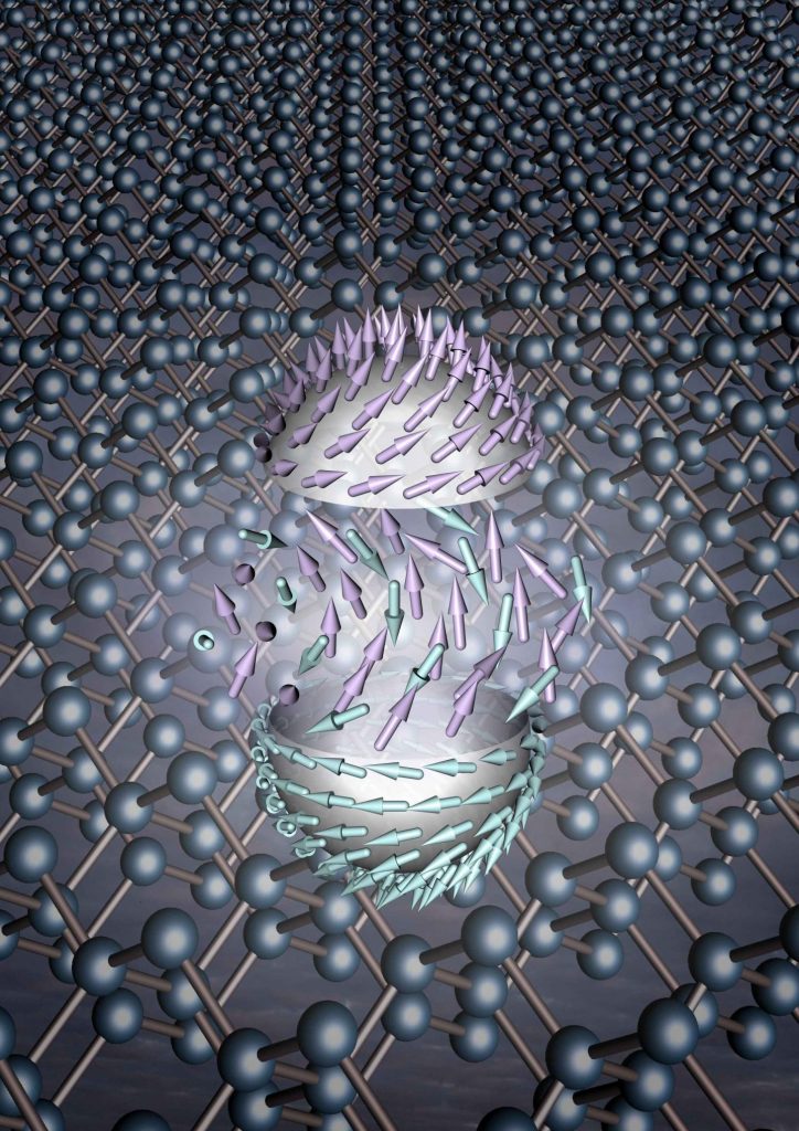
A research team at D-Wave Inc., a quantum computing company, recently created a new quantum computing system that outperforms classical computing systems on optimization problems. This system, introduced in a paper in Nature, is based on a programmable spin glass with 5,000 qubits (the quantum equivalents of bits in classical computing).

“This work validates the original hypothesis behind quantum annealing, coming full circle from some seminal experiments conducted in the 1990s,” Andrew D. King, one of the researchers who carried out the study, told Phys.org.

“These original experiments took chunks of spin-glass alloy and subjected them to varying magnetic fields, and the observations suggested that if we made a programmable quantum spin glass, it could drive down to low-energy states of optimization problems faster than analogous classical algorithms. A Science paper published in 2014 tried to verify this on a D-Wave Two processor, but no speedup was found.”

“This is a ‘full circle’ moment, in the sense that we have verified and extended the hypothesis of the UChicago [University of Chicago] and NEC [Nippon Electric Company] researchers; quantum annealing shows a scaling advantage over simulated thermal annealing,” King said. “Ours is the largest programmable quantum simulation ever performed; reproducing it classically is way beyond the reach of known methods.”

“We have a clear view of quantum effects and very clear evidence, both theoretical and experimental, that the quantum effects are conferring a computational scaling advantage over classical methods,” King said. “We want to highlight the difference between this original definition of quantum advantage and the fact that it is sometimes used as a stand-in term for quantum supremacy, which we have not demonstrated. [emphases mine] Gate-model quantum computers have not shown any capabilities approaching this for optimization, and I personally don’t believe they ever will.”

“For a long time, it was subject for debate whether or not coherent quantum dynamics were playing any role at all in quantum annealing,” King said. “While this controversy has been rebuked by previous works, this new research is the clearest demonstration yet, by far.”

An April 19, 2023 D-Wave Systems news release, which seems to have been the basis for Fadelli’s article, provides more detail in a release that functions as a research announcement and a sales tool, Note: Links have been removed,

D-Wave Quantum Inc. (NYSE: QBTS), a leader in quantum computing systems, software, and services—and the only provider building both annealing and gate-model quantum computers, today published a peer-reviewed milestone paper showing the performance of its 5,000 qubit Advantage™ quantum computer is significantly faster than classical compute on 3D spin glass optimization problems, an intractable class of optimization problems. This paper also represents the largest programmable quantum simulation reported to date.

The paper—a collaboration between scientists from D-Wave and Boston University—entitled “Quantum critical dynamics in a 5,000-qubit programmable spin glass,” was published in the peer-reviewed journal Nature today and is available here. Building upon research conducted on up to 2,000 qubits last September, the study shows that the D-Wave quantum processor can compute coherent quantum dynamics in large-scale optimization problems. This work was done using D-Wave’s commercial-grade annealing-based quantum computer, which is accessible for customers to use today.

With immediate implications to optimization, the findings show that coherent quantum annealing can improve solution quality faster than classical algorithms. The observed speedup matches the theory of coherent quantum annealing and shows​ a direct connection between coherence and the core computational power of quantum annealing.

“This research marks a significant achievement for quantum technology, as it demonstrates a computational advantage over classical approaches for an intractable class of optimization problems,” said Dr. Alan Baratz, CEO of D-Wave. “For those seeking evidence of quantum annealing’s unrivaled performance, this work offers definitive proof.

This work supports D-Wave’s ongoing commitment to relentless scientific innovation and product delivery, as the company continues development on its future annealing and gate model quantum computers. To date, D-Wave has brought to market five generations of quantum computers and launched an experimental prototype of its sixth-generation machine, the Advantage2™ system, in June 2022. The full Advantage2 system is expected to feature 7,000+ qubits, 20-way connectivity and higher coherence to solve even larger and more complex problems. Read more about the research in our Medium post here.

Paper’s Authors and Leading Industry Voices Echo Support

“This is an important advance in the study of quantum phase transitions on quantum annealers. It heralds a revolution in experimental many-body physics and bodes well for practical applications of quantum computing,” said Wojciech Zurek, theoretical physicist at Los Alamos National Laboratory and leading authority on quantum theory. Dr. Zurek is widely renowned for his groundbreaking contribution to our understanding of the early universe as well as condensed matter systems through the discovery of the celebrated Kibble-Zurek mechanism. This mechanism underpins the physics behind the experiment reported in this paper. “The same hardware that has already provided useful experimental proving ground for quantum critical dynamics can be also employed to seek low-energy states that assist in finding solutions to optimization problems.”

“Disordered magnets, such as spin glasses, have long functioned as model systems for testing solvers of complex optimization problems,” said Gabriel Aeppli, professor of physics at ETH Zürich and EPF Lausanne, and head of the Photon Science Division of the Paul Scherrer Institut. Professor Aeppli coauthored the first experimental paper demonstrating advantage of quantum annealing over thermal annealing in reaching ground state of disordered magnets. “This paper gives evidence that the quantum dynamics of a dedicated hardware platform are faster than for known classical algorithms to find the preferred, lowest energy state of a spin glass, and so promises to continue to fuel the further development of quantum annealers for dealing with practical problems.”

“As a physicist who has built my career on computer simulations of quantum systems, it has been amazing to experience first-hand the transformative capabilities of quantum annealing devices,” said Anders Sandvik, professor of physics at Boston University and a coauthor of the paper. “This paper already demonstrates complex quantum dynamics on a scale beyond any classical simulation method, and I’m very excited about the expected enhanced performance of future devices. I believe we are now entering an era when quantum annealing becomes an essential tool for research on complex systems.”

“This work marks a major step towards large-scale quantum simulations of complex materials,” said Hidetoshi Nishimori, Professor, Institute of Innovative Research, Tokyo Institute of Technology and one of the original inventors of quantum annealing. “We can now expect novel physical phenomena to be revealed by quantum simulations using quantum annealing, ultimately leading to the design of materials of significant societal value.”

“This represents some of the most important experimental work ever performed in quantum optimization,” said Dr. Andrew King, director of performance research at D-Wave. “We’ve demonstrated a speedup over simulated annealing, in strong agreement with theory, providing high-quality solutions for large-scale problems. This work shows clear evidence of quantum dynamics in optimization, which we believe paves the way for even more complex problem-solving using quantum annealing in the future. The work exhibits a programmable realization of lab experiments that originally motivated quantum annealing 25 years ago.”

“Not only is this the largest demonstration of quantum simulation to date, but it also provides the first experimental evidence, backed by theory, that coherent quantum dynamics can accelerate the attainment of better solutions in quantum annealing,” said Mohammad Amin, fellow, quantum algorithms and systems, at D-Wave. “The observed speedup can be attributed to complex critical dynamics during quantum phase transition, which cannot be replicated by classical annealing algorithms, and the agreement between theory and experiment is remarkable. We believe these findings have significant implications for quantum optimization, with practical applications in addressing real-world problems.”

About D-Wave Quantum Inc.

D-Wave is a leader in the development and delivery of quantum computing systems, software, and services, and is the world’s first commercial supplier of quantum computers—and the only company building both annealing quantum computers and gate-model quantum computers. Our mission is to unlock the power of quantum computing today to benefit business and society. We do this by delivering customer value with practical quantum applications for problems as diverse as logistics, artificial intelligence, materials sciences, drug discovery, scheduling, cybersecurity, fault detection, and financial modeling. D-Wave’s technology is being used by some of the world’s most advanced organizations, including Volkswagen, Mastercard, Deloitte, Davidson Technologies, ArcelorMittal, Siemens Healthineers, Unisys, NEC Corporation, Pattison Food Group Ltd., DENSO, Lockheed Martin, Forschungszentrum Jülich, University of Southern California, and Los Alamos National Laboratory.

Forward-Looking Statements

This press release contains forward-looking statements within the meaning of the Private Securities Litigation Reform Act of 1995, which statements are based on beliefs and assumptions and on information currently available. In some cases, you can identify forward-looking statements by the following words: “may,” “will,” “could,” “would,” “should,” “expect,” “intend,” “plan,” “anticipate,” “believe,” “estimate,” “predict,” “project,” “potential,” “continue,” “ongoing,” or the negative of these terms or other comparable terminology, although not all forward-looking statements contain these words. These statements involve risks, uncertainties, and other factors that may cause actual results, levels of activity, performance, or achievements to be materially different from the information expressed or implied by these forward-looking statements. We caution you that these statements are based on a combination of facts and factors currently known by us and our projections of the future, which are subject to a number of risks. Forward-looking statements in this press release include, but are not limited to, statements regarding the impact of the results of this study; the company’s Advantage2™ experimental prototype; and the potential for future problem-solving using quantum annealing. We cannot assure you that the forward-looking statements in this press release will prove to be accurate. These forward-looking statements are subject to a number of risks and uncertainties, including, among others, various factors beyond management’s control, including general economic conditions and other risks, our ability to expand our customer base and the customer adoption of our solutions, and the uncertainties and factors set forth in the sections entitled “Risk Factors” and “Cautionary Note Regarding Forward-Looking Statements” in D-Wave Quantum Inc.’s Form S-4 Registration Statement, as amended, previously filed with the Securities and Exchange Commission, as well as factors associated with companies, such as D-Wave, that are engaged in the business of quantum computing, including anticipated trends, growth rates, and challenges in those businesses and in the markets in which they operate; the outcome of any legal proceedings that may be instituted against us; risks related to the performance of our business and the timing of expected business or financial milestones; unanticipated technological or project development challenges, including with respect to the cost and or timing thereof; the performance of the our products; the effects of competition on our business; the risk that we will need to raise additional capital to execute our business plan, which may not be available on acceptable terms or at all; the risk that we may never achieve or sustain profitability; the risk that we are unable to secure or protect our intellectual property; volatility in the price of our securities; and the risk that our securities will not maintain the listing on the NYSE. Furthermore, if the forward-looking statements contained in this press release prove to be inaccurate, the inaccuracy may be material. In addition, you are cautioned that past performance may not be indicative of future results. In light of the significant uncertainties in these forward-looking statements, you should not place undue reliance on these statements in making an investment decision or regard these statements as a representation or warranty by any person we will achieve our objectives and plans in any specified time frame, or at all. The forward-looking statements in this press release represent our views as of the date of this press release. We anticipate that subsequent events and developments will cause our views to change. However, while we may elect to update these forward-looking statements at some point in the future, we have no current intention of doing so except to the extent required by applicable law. You should, therefore, not rely on these forward-looking statements as representing our views as of any date subsequent to the date of this press release.

Here’s a link to and a citation for the paper,

Quantum critical dynamics in a 5,000-qubit programmable spin glass by Andrew D. King, Jack Raymond, Trevor Lanting, Richard Harris, Alex Zucca, Fabio Altomare, Andrew J. Berkley, Kelly Boothby, Sara Ejtemaee, Colin Enderud, Emile Hoskinson, Shuiyuan Huang, Eric Ladizinsky, Allison J. R. MacDonald, Gaelen Marsden, Reza Molavi, Travis Oh, Gabriel Poulin-Lamarre, Mauricio Reis, Chris Rich, Yuki Sato, Nicholas Tsai, Mark Volkmann, Jed D. Whittaker, Jason Yao, Anders W. Sandvik & Mohammad H. Amin. Nature volume 617, pages 61–66 (2023) DOI: https://doi.org/10.1038/s41586-023-05867-2 Published: 19 April 2023 Issue Date: 04 May 2023

This paper is behind a paywall but there is an open access version on the arxiv website which means that it has had some peer review but may differ from the version in Nature.

Gilding medieaval statues with nanoscale gold sheets

The altar examined is thought to have been made around 1420 in Southern Germany and for a long time stood in a mountain chapel on Alp Leiggern in the Swiss canton of Valais. Today it is on display at the Swiss National Museum (Landesmuseum Zürich). (Photo: Swiss National Museum, Landesmuseum Zürich) [ddownloaded from https://www.psi.ch/en/media/our-research/nanomaterial-from-the-middle-ages]

As amazing as the altar appears, it was hiding some even more amazing secrets. From an October 10, 2022 Paul Scherrer Institute (PSI) press release (also on EurekAlert but published October 11, 2022) by Barbara Vonarburg,

To gild sculptures in the late Middle Ages, artists often applied ultra-thin gold foil supported by a silver base layer. For the first time, scientists at the Paul Scherrer Institute [PSI] have managed to produce nanoscale 3D images of this material, known as Zwischgold. The pictures show this was a highly sophisticated mediaeval production technique and demonstrate why restoring such precious gilded artefacts is so difficult.

The samples examined at the Swiss Light Source SLS using one of the most advanced microscopy methods were unusual even for the highly experienced PSI team: minute samples of materials taken from an altar and wooden statues originating from the fifteenth century. The altar is thought to have been made around 1420 in Southern Germany and stood for a long time in a mountain chapel on Alp Leiggern in the Swiss canton of Valais. Today it is on display at the Swiss National Museum (Landesmuseum Zürich). In the middle you can see Mary cradling Baby Jesus. The material sample was taken from a fold in the Virgin Mary’s robe. The tiny samples from the other two mediaeval structures were supplied by Basel Historical Museum.

The material was used to gild the sacred figures. It is not actually gold leaf, but a special double-sided foil of gold and silver where the gold can be ultra-thin because it is supported by the silver base. This material, known as Zwischgold (part-gold) was significantly cheaper than using pure gold leaf. “Although Zwischgold was frequently used in the Middle Ages, very little was known about this material up to now,” says PSI physicist Benjamin Watts: “So we wanted to investigate the samples using 3D technology which can visualise extremely fine details.” Although other microscopy techniques had been used previously to examine Zwischgold, they only provided a 2D cross-section through the material. In other words, it was only possible to view the surface of the cut segment, rather than looking inside the material.  The scientists were also worried that cutting through it may have changed the structure of the sample. The advanced microscopy imaging method used today, ptychographic tomography, provides a 3D image of Zwischgold’s exact composition for the first time.

X-rays generate a diffraction pattern

The PSI scientists conducted their research using X-rays produced by the Swiss Light Source SLS. These produce tomographs displaying details in the nanoscale range – millionths of a millimetre, in other words. “Ptychography is a fairly sophisticated method, as there is no objective lens that forms an image directly on the detector,” Watts explains. Ptychography actually produces a diffraction pattern of the illuminated area, in other words an image with points of differing intensity. By manipulating the sample in a precisely defined manner, it is possible to generate hundreds of overlapping diffraction patterns. “We can then combine these diffraction patterns like a sort of giant Sudoku puzzle and work out what the original image looked like,” says the physicist. A set of ptychographic images taken from different directions can be combined to create a 3D tomogram.

The advantage of this method is its extremely high resolution. “We knew the thickness of the Zwischgold sample taken from Mary was of the order of hundreds of nanometres,” Watts explains. “So we had to be able to reveal even tinier details.” The scientists achieved this using ptychographic tomography, as they report in their latest article in the journal Nanoscale. “The 3D images clearly show how thinly and evenly the gold layer is over the silver base layer,” says Qing Wu, lead author of the publication. The art historian and conservation scientist completed her PhD at the University of Zurich, in collaboration with PSI and the Swiss National Museum. “Many people had assumed that technology in the Middle Ages was not particularly advanced,” Wu comments. “On the contrary: this was not the Dark Ages, but a period when metallurgy and gilding techniques were incredibly well developed.”

Secret recipe revealed

Unfortunately there are no records of how Zwischgold was produced at the time. “We reckon the artisans kept their recipe secret,” says Wu. Based on nanoscale images and documents from later epochs, however, the art historian now knows the method used in the 15th century: first the gold and the silver were hammered separately to produce thin foils, whereby the gold film had to be much thinner than the silver. Then the two metal foils were worked on together. Wu describes the process: “This required special beating tools and pouches with various inserts made of different materials into which the foils were inserted,” Wu explains. This was a fairly complicated procedure that required highly skilled specialists.

“Our investigations of Zwischgold samples showed the average thickness of the gold layer to be around 30 nanometres, while gold leaf produced in the same period and region was approximately 140 nanometres thick,” Wu explains. “This method saved on gold, which was much more expensive”. At the same time, there was also a very strict hierarchy of materials: gold leaf was used to make the halo of one figure, for example, while Zwischgold was used for the robe. Because this material has less of a sheen, the artists often used it to colour the hair or beards of their statues. “It is incredible how someone with only hand tools was able to craft such nanoscale material,” Watts says. Mediaeval artisans also benefited from a unique property of gold and silver crystals when pressed together: their morphology is preserved across the entire metal film. “A lucky coincidence of nature that ensures this technique works,” says the physicist.

Golden surface turns black

The 3D images do bring to light one drawback of using Zwischgold, however: the silver can push through the gold layer and cover it. The silver moves surprisingly quickly – even at room temperature. Within days, a thin silver coating covers the gold completely. At the surface the silver comes into contact with water and sulphur in the air, and corrodes. “This makes the gold surface of the Zwischgold turn black over time,” Watts explains. “The only thing you can do about this is to seal the surface with a varnish so the sulphur does not attack the silver and form silver sulphide.” The artisans using Zwischgold were aware of this problem from the start. They used resin, glue or other organic substances as a varnish. “But over hundreds of years this protective layer has decomposed, allowing corrosion to continue,” Wu explains.

The corrosion also encourages more and more silver to migrate to the surface, creating a gap below the Zwischgold. “We were surprised how clearly this gap under the metal layer could be seen,” says Watts. Especially in the sample taken from Mary’s robe, the Zwischgold had clearly come away from the base layer. “This gap can cause mechanical instability, and we expect that in some cases it is only the protective coating over the Zwischgold that is holding the metal foil in place,” Wu warns. This is a massive problem for the restoration of historical artefacts, as the silver sulphide has become embedded in the varnish layer or even further down. “If we remove the unsightly products of corrosion, the varnish layer will also fall away and we will lose everything,” says Wu. She hopes it will be possible in future to develop a special material that can be used to fill the gap and keep the Zwischgold attached. “Using ptychographic tomography, we could check how well such a consolidation material would perform its task,” says the art historian.

About PSI

The Paul Scherrer Institute PSI develops, builds and operates large, complex research facilities and makes them available to the national and international research community. The institute’s own key research priorities are in the fields of matter and materials, energy and environment and human health. PSI is committed to the training of future generations. Therefore about one quarter of our staff are post-docs, post-graduates or apprentices. Altogether PSI employs 2100 people, thus being the largest research institute in Switzerland. The annual budget amounts to approximately CHF 400 million. PSI is part of the ETH Domain, with the other members being the two Swiss Federal Institutes of Technology, ETH Zurich and EPFL Lausanne, as well as Eawag (Swiss Federal Institute of Aquatic Science and Technology), Empa (Swiss Federal Laboratories for Materials Science and Technology) and WSL (Swiss Federal Institute for Forest, Snow and Landscape Research). Insight into the exciting research of the PSI with changing focal points is provided 3 times a year in the publication 5232 – The Magazine of the Paul Scherrer Institute.

Here’s a link to and a citation for the paper,

A modern look at a medieval bilayer metal leaf: nanotomography of Zwischgold by
Qing Wu, Karolina Soppa, Elisabeth Müller, Julian Müller, Michal Odstrcil, Esther Hsiao Rho Tsai, Andreas Späth, Mirko Holler, Manuel Guizar-Sicairos, Benjamin Butz, Rainer H. Fink, and Benjamin Watts. Nanoscale DOI: https://doi.org/10.1039/D2NR03367D First published: 10 Oct 2022

This paper is open access.

Skyrmions (nanoscale vortices) with a unique property

A Sept. 23, 2020 news item on Nanowerk describes both skyrmions and the latest in potentially practical ‘skyrmion research’ ,

Nanoscale vortices known as skyrmions can be created in many magnetic materials. For the first time, researchers at PSI [Paul Scherrer Institute] have managed to create and identify antiferromagnetic skyrmions with a unique property: critical elements inside them are arranged in opposing directions. Scientists have succeeded in visualising this phenomenon using neutron scattering. Their discovery is a major step towards developing potential new applications, such as more efficient computers.

Caption: Skyrmions are nanoscale vortices in the magnetic alignment of atoms. For the first time, PSI researchers have now created antiferromagnetic skyrmions in which critical spins are arranged in opposing directions. This state is shown in the artist’s impression above. Credit: Paul Scherrer Institute/Diego Rosales

That image makes me think of ‘op art’. For anyone unfamiliar with the art movement, there’s Bob Lansroth’s October 29, 2015 article (10 Op Art Artists Whose Work You Have to Follow) for widwalls.ch,

The nature of perception, optical effects, illusions and visual stimuli have been fascinating artists for many centuries. Optical Art, or Op Art, is relying on optical illusions and is sometimes even referred to as retinal art. Some critics would even call it a mathematically-themed form of Abstract Art, considering the use of repetitive forms and colors in order to create vibrating effects, foreground-background confusion and an exaggerated sense of depth.

Lansroth’s October 29, 2015 article is liberally illustrated with examples.

Getting back to the skyrmions at hand, a Sept. 23, 2020 Paul Scherrer Institute (PSI) press release (also on EurekAlert) by Laura Hennemann, which originated the news item, describes the research in more detail,

Whether a material is magnetic depends on the spins of its atoms. The best way to think of spins is as minute bar magnets. In a crystal structure where the atoms have fixed positions in a lattice, these spins can be arranged in criss-cross fashion or aligned all in parallel like the spears of a Roman legion, depending on the individual material and its state.

Under certain conditions it is possible to generate tiny vortices within the corps of spins. These are known as skyrmions. Scientists are particularly interested in skyrmions as a key component in future technologies, such as more efficient data storage and transfer. For example, they could be used as memory bits: a skyrmion could represent the digital one, and its absence a digital zero. As skyrmions are significantly smaller than the bits used in conventional storage media, data density is much higher and potentially also more energy efficient, while read and write operations would be faster as well. Skyrmions could therefore be useful both in classical data processing and in cutting-edge quantum computing.

Another interesting aspect for the application is that skyrmions can be created and controlled in many materials by applying an electrical current. “With existing skyrmions, however, it is tricky to move them systematically from A to B, as they tend to deviate from a straight path due to their inherent properties,” explains Oksana Zaharko, research group leader at PSI.

Working with researchers from other institutions, Dr Zaharko and her team have now created a new type of skyrmion and demonstrated a unique characteristic: in their interior, critical spins are arranged in opposite directions to one another. The researchers therefore describe their skyrmions as antiferromagnetic.

In a straight line from A to B

“One of the key advantages of antiferromagnetic skyrmions is that they are much simpler to control: if an electrical current is applied, they move in a simple straight line,” Zaharko comments. This is a major advantage: for skyrmions to be suitable for practical applications, it must be possible to selectively manipulate and position them.

The scientists created their new type of skyrmion by fabricating them in a customised antiferromagnetic crystal. Zaharko explains: “Antiferromagnetic means that adjacent spins are in an antiparallel arrangement, in other words one pointing upwards and the next pointing downwards. So what was initially observed as a property of the material we subsequently identified within the individual skyrmions as well.”

Several steps are still needed before antiferromagnetic skyrmions are mature enough for a technological application: PSI researchers had to cool the crystal down to around minus 272 degrees Celsius and apply an extremely strong magnetic field of three tesla – roughly 100,000 times the strength of the Earth’s magnetic field.

Neutron scattering to visualise the skyrmions

And the researchers have yet to create individual antiferromagnetic skyrmions. To verify the tiny vortices, the scientists are using the Swiss Spallation Neutron Source SINQ at PSI. “Here we can visualise skyrmions using neutron scattering if we have a lot of them in a regular pattern in a particular material”, Zaharko explains.

But the scientist is optimistic: “In my experience, if we manage to create skyrmions in a regular alignment, someone will soon manage to create such skyrmions individually.”

The general consensus in the research community is that once individual antiferromagnetic skyrmions can be created at room temperature, a practical application will not be far off.

Here’s a link to and a citation for the paper,

Fractional antiferromagnetic skyrmion lattice induced by anisotropic couplings by Shang Gao, H. Diego Rosales, Flavia A. Gómez Albarracín, Vladimir Tsurkan, Guratinder Kaur, Tom Fennell, Paul Steffens, Martin Boehm, Petr Čermák, Astrid Schneidewind, Eric Ressouche, Daniel C. Cabra, Christian Rüegg & Oksana Zaharko. Nature (2020) DOI: https://doi.org/10.1038/s41586-020-2716-8 Published: 23 September 2020

This paper is behind a paywall.

The Weyl fermion and new electronics

This story concerns a quasiparticle (Weyl fermion) which is a different kind of particle than the nanoparticles usually mentioned here. A March 17, 2016 news item on Nanowerk profiles research that suggests the Weyl fermion may find applications in the field of electronics,

The Weyl fermion, just discovered in the past year, moves through materials practically without resistance. Now researchers are showing how it could be put to use in electronic components.

Today electronic devices consume a lot of energy and require elaborate cooling mechanisms. One approach for the development of future energy-saving electronics is to use special particles that exist only in the interior of materials but can move there practically undisturbed. Electronic components based on these so-called Weyl fermions would consume considerably less energy than present-day chips. That’s because up to now devices have relied on the movement of electrons, which is inhibited by resistance and thus wastes energy.

Evidence for Weyl fermions was discovered only in the past year, by several research teams including scientists from the Paul Scherrer Institute (PSI). Now PSI researchers have shown — within the framework of an international collaboration with two research institutions in China and the two Swiss technical universities, ETH Zurich and EPF Lausanne — that there are materials in which only one kind of Weyl fermion exists. That could prove decisive for applications in electronic components, because it makes it possible to guide the particles’ flow in the material.

A March 17, 2016 Paul Scherrer Institute (PSI) press release by Paul Piwnicki, which originated the news item, describes the work in more detail (Note: There is some redundancy),

In the past year, researchers of the Paul Scherrer Institute PSI were among those who found experimental evidence for a particle whose existence had been predicted in the 1920s — the Weyl fermion. One of the particle’s peculiarities is that it can only exist in the interior of materials. Now the PSI researchers, together with colleagues at two Chinese research institutions as well as at ETH Zurich and EPF Lausanne, have made a subsequent discovery that opens the possibility of using the movement of Weyl fermions in future electronic devices. …

Today’s computer chips use the flow of electrons that move through the device’s conductive channels. Because, along the way, electrons are always colliding with each other or with other particles in the material, a relatively high amount of energy is needed to maintain the flow. That means not only that the device wastes a lot of energy, but also that it heats itself up enough to necessitate an elaborate cooling mechanism, which in turn requires additional space and energy.

In contrast, Weyl fermions move virtually undisturbed through the material and thus encounter practically no resistance. “You can compare it to driving on a highway where all of the cars are moving freely in the same direction,” explains Ming Shi, a senior scientist at the PSI. “The electron flow in present-day chips is more comparable to driving in congested city traffic, with cars coming from all directions and getting in each other’s way.”

Important for electronics: only one kind of particle

While in the materials examined last year there were always several kinds of Weyl fermions, all moving in different ways, the PSI researchers and their colleagues have now produced a material in which only one kind of Weyl fermion occurs. “This is important for applications in electronics, because here you must be able to precisely steer the particle flow,” explains Nan Xu, a postdoctoral researcher at the PSI.

Weyl fermions are named for the German mathematician Hermann Weyl, who predicted their existence in 1929. These particles have some striking characteristics, such as having no mass and moving at the speed of light. Weyl fermions were observed as quasiparticles in so-called Weyl semimetals. In contrast to “real” particles, quasiparticles can only exist inside materials. Weyl fermions are generated through the collective motion of electrons in suitable materials. In general, quasiparticles can be compared to waves on the surface of a body of water — without the water, the waves would not exist. At the same time, their movement is independent of the water’s motion.

The material that the researchers have now investigated is a compound of the chemical elements tantalum and phosphorus, with the chemical formula TaP. The crucial experiments were carried out with X-rays at the Swiss Light Source (SLS) of the Paul Scherrer Institute.

Studying novel materials with properties that could make them useful in future electronic devices is a central research area of the Paul Scherrer Institute. In the process, the researchers pursue a variety of approaches and use many different experimental methods.

Here’s a link to and a citation for the paper,

Observation of Weyl nodes and Fermi arcs in tantalum phosphide by N. Xu, H. M. Weng, B. Q. Lv, C. E. Matt, J. Park, F. Bisti, V. N. Strocov, D. Gawryluk, E. Pomjakushina, K. Conder, N. C. Plumb, M. Radovic, G. Autès, O. V. Yazyev, Z. Fang, X. Dai, T. Qian, J. Mesot, H. Ding & M. Shi. Nature Communications 7, Article number: 11006  doi:10.1038/ncomms11006 Published 17 March 2016

This paper is open access.