Tag Archives: photons

Testing technology for a global quantum network

This work on quantum networks comes from a joint Singapore/UK research project, from a June 2, 2016 news item on ScienceDaily,

You can’t sign up for the quantum internet just yet, but researchers have reported a major experimental milestone towards building a global quantum network — and it’s happening in space.

With a network that carries information in the quantum properties of single particles, you can create secure keys for secret messaging and potentially connect powerful quantum computers in the future. But scientists think you will need equipment in space to get global reach.

Researchers from the National University of Singapore (NUS) and the University of Strathclyde, UK, have become the first to test in orbit technology for satellite-based quantum network nodes.

They have put a compact device carrying components used in quantum communication and computing into orbit. And it works: the team report first data in a paper published 31 May 2016 in the journal Physical Review Applied.

A June 2, 2016 National University of Singapore press release, which originated the news item, provides more detail,

The team’s device, dubbed SPEQS, creates and measures pairs of light particles, called photons. Results from space show that SPEQS is making pairs of photons with correlated properties – an indicator of performance.

Team-leader Alexander Ling, an Assistant Professor at the Centre for Quantum Technologies (CQT) at NUS said, “This is the first time anyone has tested this kind of quantum technology in space.”

The team had to be inventive to redesign a delicate, table-top quantum setup to be small and robust enough to fly inside a nanosatellite only the size of a shoebox. The whole satellite weighs just 1.65-kilogramme.

Towards entanglement

Making correlated photons is a precursor to creating entangled photons. Described by Einstein as “spooky action at a distance”, entanglement is a connection between quantum particles that lends security to communication and power to computing.

Professor Artur Ekert, Director of CQT, invented the idea of using entangled particles for cryptography. He said, “Alex and his team are taking entanglement, literally, to a new level. Their experiments will pave the road to secure quantum communication and distributed quantum computation on a global scale. I am happy to see that Singapore is one of the world leaders in this area.”

Local quantum networks already exist [emphasis mine]. The problem Ling’s team aims to solve is a distance limit. Losses limit quantum signals sent through air at ground level or optical fibre to a few hundred kilometers – but we might ultimately use entangled photons beamed from satellites to connect points on opposite sides of the planet. Although photons from satellites still have to travel through the atmosphere, going top-to-bottom is roughly equivalent to going only 10 kilometres at ground level.

The group’s first device is a technology pathfinder. It takes photons from a BluRay laser and splits them into two, then measures the pair’s properties, all on board the satellite. To do this it contains a laser diode, crystals, mirrors and photon detectors carefully aligned inside an aluminum block. This sits on top of a 10 centimetres by 10 centimetres printed circuit board packed with control electronics.

Through a series of pre-launch tests – and one unfortunate incident – the team became more confident that their design could survive a rocket launch and space conditions. The team had a device in the October 2014 Orbital-3 rocket which exploded on the launch pad. The satellite containing that first device was later found on a beach intact and still in working order.

Future plans

Even with the success of the more recent mission, a global network is still a few milestones away. The team’s roadmap calls for a series of launches, with the next space-bound SPEQS slated to produce entangled photons. SPEQS stands for Small Photon-Entangling Quantum System.

With later satellites, the researchers will try sending entangled photons to Earth and to other satellites. The team are working with standard “CubeSat” nanosatellites, which can get relatively cheap rides into space as rocket ballast. Ultimately, completing a global network would mean having a fleet of satellites in orbit and an array of ground stations.

In the meantime, quantum satellites could also carry out fundamental experiments – for example, testing entanglement over distances bigger than Earth-bound scientists can manage. “We are reaching the limits of how precisely we can test quantum theory on Earth,” said co-author Dr Daniel Oi at the University of Strathclyde.

Here’s a link to and a citation for the paper,

Generation and Analysis of Correlated Pairs of Photons aboard a Nanosatellite by Zhongkan Tang, Rakhitha Chandrasekara, Yue Chuan Tan, Cliff Cheng, Luo Sha, Goh Cher Hiang, Daniel K. L. Oi, and Alexander Ling. Phys. Rev. Applied 5, 054022 DOI: http://dx.doi.org/10.1103/PhysRevApplied.5.054022 Published 31 May 2016

This paper is behind a paywall.
Light-captured energetics (harvesting light for optoelectronics)

Comparing graphene to a tiger is unusual but that’s what researcher Sanfeng Wu does—eventually—in a May 13, 2016 University of Washington news release (also on EurekAlert) about his work,

In the quest to harvest light for electronics, the focal point is the moment when photons — light particles — encounter electrons, those negatively-charged subatomic particles that form the basis of our modern electronic lives. If conditions are right when electrons and photons meet, an exchange of energy can occur. Maximizing that transfer of energy is the key to making efficient light-captured energetics possible.

“This is the ideal, but finding high efficiency is very difficult,” said University of Washington physics doctoral student Sanfeng Wu. “Researchers have been looking for materials that will let them do this — one way is to make each absorbed photon transfer all of its energy to many electrons, instead of just one electron in traditional devices.”

In traditional light-harvesting methods, energy from one photon only excites one electron or none depending on the absorber’s energy gap, transferring just a small portion of light energy into electricity. The remaining energy is lost as heat. But in a paper released May 13 in Science Advances, Wu, UW associate professor Xiaodong Xu and colleagues at four other institutions describe one promising approach to coax photons into stimulating multiple electrons. Their method exploits some surprising quantum-level interactions to give one photon multiple potential electron partners. Wu and Xu, who has appointments in the UW’s Department of Materials Science & Engineering and the Department of Physics, made this surprising discovery using graphene.

There has been intense research on graphene’s electrical properties but the researchers’ discovery adds a new property to be investigated (from the news release),

“Graphene is a substance with many exciting properties,” said Wu, the paper’s lead author. “For our purposes, it shows a very efficient interaction with light.”

Graphene is a two-dimensional hexagonal lattice of carbon atoms bonded to one another, and electrons are able to move easily within graphene. The researchers took a single layer of graphene — just one sheet of carbon atoms thick — and sandwiched it between two thin layers of a material called boron-nitride.

Boron-nitride is a material that has excited a great deal of interest in the last 12 to 18 months (from the news release),

“Boron-nitride has a lattice structure that is very similar to graphene, but has very different chemical properties,” said Wu. “Electrons do not flow easily within boron-nitride; it essentially acts as an insulator.”

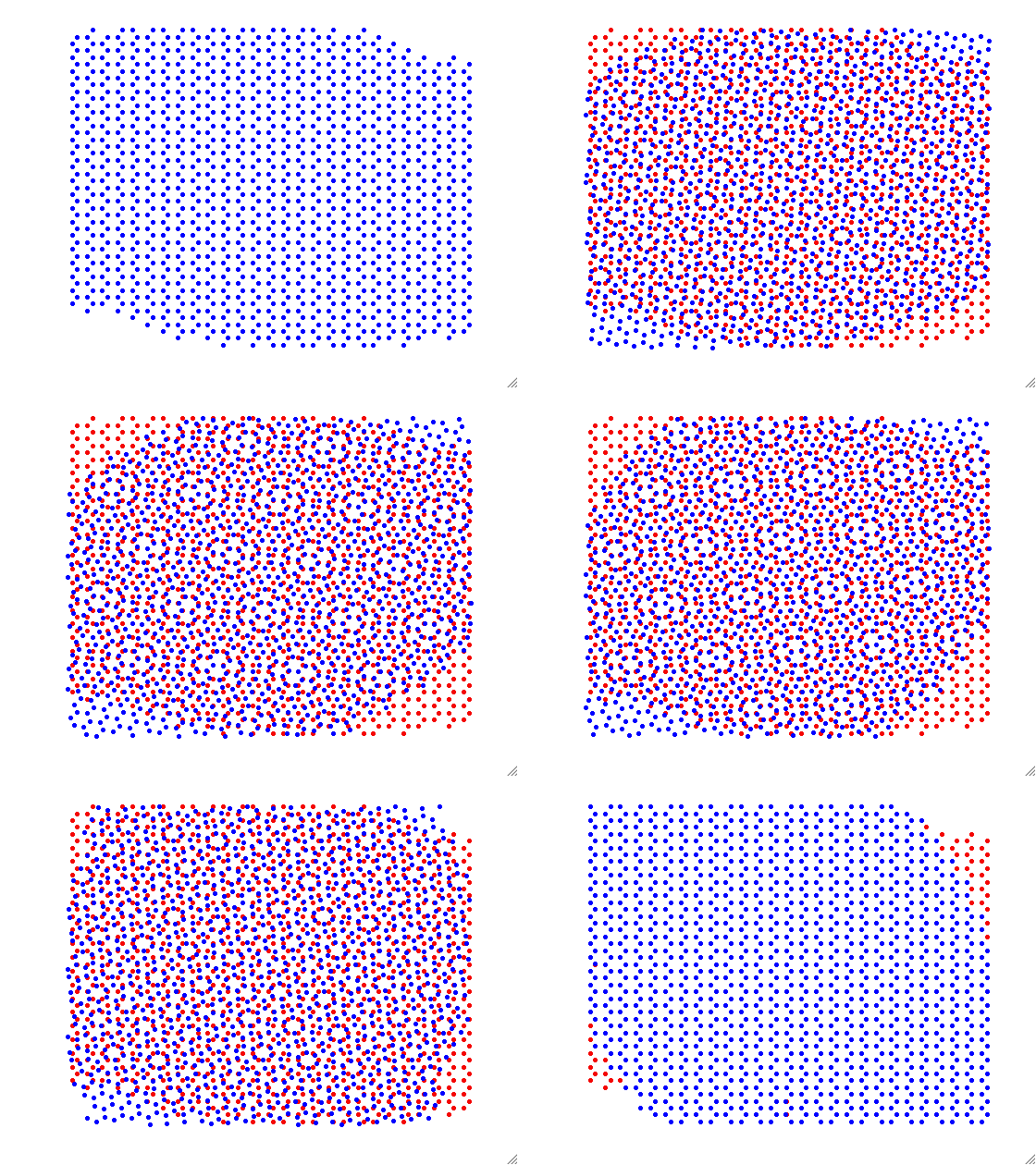
Xu and Wu discovered that when the graphene layer’s lattice is aligned with the layers of boron-nitride, a type of “superlattice” is created with properties allowing efficient optoelectronics that researchers had sought. These properties rely on quantum mechanics, the occasionally baffling rules that govern interactions between all known particles of matter. Wu and Xu detected unique quantum regions within the superlattice known as Van Hove singularities.

Here’s an animated .gif illustrating the superlattice in action,

The Moire superlattice they created by aligning graphene and boron-nitride. Credit: Sanfeng Wu.

The Moire superlattice they created by aligning graphene and boron-nitride. Credit: Sanfeng Wu.

The news release goes on to describe the Van Hove singularities within the superlattice and to mention the ‘tiger’,

“These are regions of huge electron density of states, and they were not accessed in either the graphene or boron-nitride alone,” said Wu. “We only created these high electron density regions in an accessible way when both layers were aligned together.”

When Xu and Wu directed energetic photons toward the superlattice, they discovered that those Van Hove singularities were sites where one energized photon could transfer its energy to multiple electrons that are subsequently collected by electrodes— not just one electron or none with the remaining energy lost as heat. By a conservative estimate, Xu and Wu report that within this superlattice one photon could “kick” as many as five electrons to flow as current.

With the discovery of collecting multiple electrons upon the absorption of one photon, researchers may be able to create highly efficient devices that could harvest light with a large energy profit. Future work would need to uncover how to organize the excited electrons into electrical current for optimizing the energy-converting efficiency and remove some of the more cumbersome properties of their superlattice, such as the need for a magnetic field. But they believe this efficient process between photons and electrons represents major progress.

“Graphene is a tiger with great potential for optoelectronics, but locked in a cage,” said Wu. “The singularities in this superlattice are a key to unlocking that cage and releasing graphene’s potential for light harvesting application.”

H/t to a May 13, 2016 news item on phys.org.

Here’s a link to and a citation for the paper,

Multiple hot-carrier collection in photo-excited graphene Moiré superlattices by Sanfeng Wu, Lei Wang, You Lai, Wen-Yu Shan, Grant Aivazian, Xian Zhang, Takashi Taniguchi, Kenji Watanabe, Di Xiao, Cory Dean, James Hone, Zhiqiang Li, and Xiaodong Xu. Science Advances 13 May 2016: Vol. 2, no. 5, e1600002 DOI: 10.1126/sciadv.1600002

This paper is open access.

New tool for mapping neuronal connections in the brain

This work comes from the US Naval Research Laboratory according to a Nov. 17, 2015 news item on Nanowerk (Note: A link has been removed),

Research biologists, chemists and theoreticians at the U.S. Naval Research Laboratory (NRL), are on pace to develop the next generation of functional materials that could enable the mapping of the complex neural connections in the brain (“Electric Field Modulation of Semiconductor Quantum Dot Photoluminescence: Insights Into the Design of Robust Voltage-Sensitive Cellular Imaging Probes”). The ultimate goal is to better understand how the billions of neurons in the brain communicate with one another during normal brain function, or dysfunction, as result of injury or disease.

“There is tremendous interest in mapping all the neuron connections in the human brain,” said Dr. James Delehanty, research biologist, Center for Biomolecular Science and Engineering. “To do that we need new tools or materials that allow us to see how large groups of neurons communicate with one another while, at the same time, being able to focus in on a single neuron’s activity. Our most recent work potentially opens the integration of voltage-sensitive nanomaterials into live cells and tissues in a variety of configurations to achieve real-time imaging capabilities not currently possible.”

A Nov. 17, 2015 US Naval Research Laboratory (NRL) news release on EurekAlert, which originated the news item, provides more details,

The basis of neuron communication is the time-dependent modulation of the strength of the electric field that is maintained across the cell’s plasma membrane. This is called an action potential. Among the nanomaterials under consideration for application in neuronal action potential imaging are quantum dots (QDs) — crystalline semiconductor nanomaterials possessing a number of advantageous photophysical attributes.

“QDs are very bright and photostable so you can look at them for long times and they allow for tissue imaging configurations that are not compatible with current materials, for example, organic dyes,” Delehanty added. “Equally important, we’ve shown here that QD brightness tracks, with very high fidelity, the time-resolved electric field strength changes that occur when a neuron undergoes an action potential. Their nanoscale size make them ideal nanoscale voltage sensing materials for interfacing with neurons and other electrically active cells for voltage sensing.”

QDs are small, bright, photo-stable materials that possess nanosecond fluorescence lifetimes. They can be localized within or on cellular plasma membranes and have low cytotoxicity when interfaced with experimental brain systems. Additionally, QDs possess two-photon action cross-section orders of magnitude larger than organic dyes or fluorescent proteins. Two-photon imaging is the preferred imaging modality for imaging deep (millimeters) into the brain and other tissues of the body.

In their most recent work, the NRL researchers showed that an electric field typical of those found in neuronal membranes results in suppression of the QD photoluminescence (PL) and, for the first time, that QD PL is able to track the action potential profile of a firing neuron with millisecond time resolution. This effect is shown to be connected with electric-field-driven QD ionization and consequent QD PL quenching, in contradiction with conventional wisdom that suppression of the QD PL is attributable to the quantum confined Stark effect — the shifting and splitting of spectral lines of atoms and molecules due to presence of an external electric field.

“The inherent superior photostability properties of QDs coupled with their voltage sensitivity could prove advantageous to long-term imaging capabilities that are not currently attainable using traditional organic voltage sensitive dyes,” Delehanty said. “We anticipate that continued research will facilitate the rational design and synthesis of voltage-sensitive QD probes that can be integrated in a variety of imaging configurations for the robust functional imaging and sensing of electrically active cells.”

Here’s a link to and a citation for the paper,

Electric Field Modulation of Semiconductor Quantum Dot Photoluminescence: Insights Into the Design of Robust Voltage-Sensitive Cellular Imaging Probes by Clare E. Rowland, Kimihiro Susumu, Michael H. Stewart, Eunkeu Oh, Antti J. Mäkinen, Thomas J. O’Shaughnessy, Gary Kushto, Mason A. Wolak, Jeffrey S. Erickson, Alexander L. Efros, Alan L. Huston, and James B. Delehanty. Nano Lett., 2015, 15 (10), pp 6848–6854 DOI: 10.1021/acs.nanolett.5b02725 Publication Date (Web): September 28, 2015

Copyright © 2015 American Chemical Society

This paper is behind a paywall.

A new nanoparticle—layered* like an onion

The new nanoparticle comes courtesy of an international collaboration (US, China, Sweden, and Russia. A Nov. 10, 2015 University of Buffalo news release (also on EurekAlert) by Charlotte Hu describes the particle and its properties,

A new, onion-like nanoparticle could open new frontiers in biomaging, solar energy harvesting and light-based security techniques.

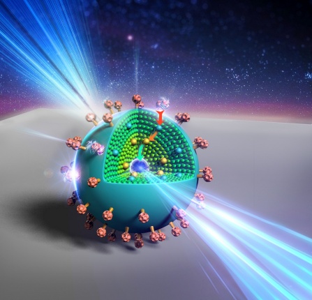
The particle’s innovation lies in its layers: a coating of organic dye, a neodymium-containing shell, and a core that incorporates ytterbium and thulium. Together, these strata convert invisible near-infrared light to higher energy blue and UV light with record-high efficiency, a trick that could improve the performance of technologies ranging from deep-tissue imaging and light-induced therapy to security inks used for printing money.

Here’s an artist’s representation of the new nanoparticle,

An artist’s rendering shows the layers of a new, onion-like nanoparticle whose specially crafted layers enable it to efficiently convert invisible near-infrared light to higher energy blue and UV light. Credit: Kaiheng Wei Courtesy: University of Buffalo

An artist’s rendering shows the layers of a new, onion-like nanoparticle whose specially crafted layers enable it to efficiently convert invisible near-infrared light to higher energy blue and UV light. Credit: Kaiheng Wei Courtesy: University of Buffalo

The news release goes on to describe technology in more detail,

When it comes to bioimaging, near-infrared light could be used to activate the light-emitting nanoparticles deep inside the body, providing high-contrast images of areas of interest. In the realm of security, nanoparticle-infused inks could be incorporated into currency designs; such ink would be invisible to the naked eye, but glow blue when hit by a low-energy laser pulse — a trait very difficult for counterfeiters to reproduce.

“It opens up multiple possibilities for the future,” says Tymish Ohulchanskyy, deputy director of photomedicine and research associate professor at the Institute for Lasers, Photonics, and Biophotonics (ILPB) at the University at Buffalo.

“By creating special layers that help transfer energy efficiently from the surface of the particle to the core, which emits blue and UV light, our design helps overcome some of the long-standing obstacles that previous technologies faced,” says Guanying Chen, professor of chemistry at Harbin Institute of Technology [China] and ILPB research associate professor.

“Our particle is about 100 times more efficient at ‘upconverting’ light than similar nanoparticles created in the past, making it much more practical,” says Jossana Damasco, a UB chemistry PhD student who played a key role in the project.

The research was published online in Nano Letters on Oct. 21 and led by the Institute for Lasers, Photonics, and Biophotonics at UB, and the Harbin Institute of Technology in China, with contributions from the Royal Institute of Technology in Sweden; Tomsk State University in Russia; and the University of Massachusetts Medical School.

The study’s senior author was Paras Prasad, ILPB executive director and SUNY [State University of New York] Distinguished Professor in chemistry, physics, medicine and electrical engineering at UB.

Peeling back the layers

Converting low-energy light to light of higher energies isn’t easy to do. The process involves capturing two or more tiny packets of light called “photons” from a low-energy light source, and combining their energy to form a single, higher-energy photon.

The onionesque nanoparticle performs this task beautifully. Each of its three layers fulfills a unique function:

  • The outermost layer is a coating of organic dye. This dye is adept at absorbing photons from low-energy near-infrared light sources. It acts as an “antenna” for the nanoparticle, harvesting light and transferring energy inside, Ohulchanskyy says.
  • The next layer is a neodymium-containing shell. This layer acts as a bridge, transferring energy from the dye to the particle’s light-emitting core.
  • Inside the light-emitting core, ytterbium and thulium ions work in concert. The ytterbium ions draw energy into the core and pass the energy on to the thulium ions, which have special properties that enable them to absorb the energy of three, four or five photons at once, and then emit a single higher-energy photon of blue and UV light.

So why not just use the core? Why add the dye and neodymium layer at all?

As Ohulchanskyy and Chen explain, the core itself is inefficient in absorbing photons from the outside world. That’s where the dye comes in.

Once you add the dye, the neodymium-containing layer is necessary for transferring energy efficiently from dye to core. Ohulchanskyy uses the analogy of a staircase to explain why this is: When molecules or ions in a material absorb a photon, they enter an “excited” state from which they can transfer energy to other molecules or ions. The most efficient transfer occurs between molecules or ions whose excited states require a similar amount of energy to obtain, but the dye and ytterbium ions have excited states with very different energies. So the team added neodymium — whose excited state is in between that of the dye and thulium’s — to act as a bridge between the two, creating a “staircase” for the energy to travel down to reach emitting thulium ions.

Here’s a link to and a citation for the paper,

Energy-Cascaded Upconversion in an Organic Dye-Sensitized Core/Shell Fluoride Nanocrystal by Guanying Chen, Jossana Damasco, Hailong Qiu, Wei Shao, Tymish Y. Ohulchanskyy, Rashid R. Valiev, Xiang Wu, Gang Han, Yan Wang, Chunhui Yang, Hans Ågren, and Paras N. Prasad. Nano Lett., 2015, 15 (11), pp 7400–7407 DOI: 10.1021/acs.nanolett.5b02830 Publication Date (Web): October 21, 2015

Copyright © 2015 American Chemical Society

This paper is behind a paywall.

Finally, there is a Nov. 11, 2015 article about the research by Jake Wilkinson for Azonano. He provides additional details such as this measurement,

Measuring approximately 50nm in diameter, the new nanoparticle features three differently designed layers. …

*’ayered’ changed to ‘layered’ on Nov. 11, 2015.

US National Institute of Standards and Technology and molecules made of light (lightsabres anyone?)

As I recall, lightsabres are a Star Wars invention. I gather we’re a long way from running around with lightsabres  but there is hope, if that should be your dream, according to a Sept. 9, 2015 news item on Nanowerk,

… a team including theoretical physicists from JQI [Joint Quantum Institute] and NIST [US National Institute of Stnadards and Technology] has taken another step toward building objects out of photons, and the findings hint that weightless particles of light can be joined into a sort of “molecule” with its own peculiar force.

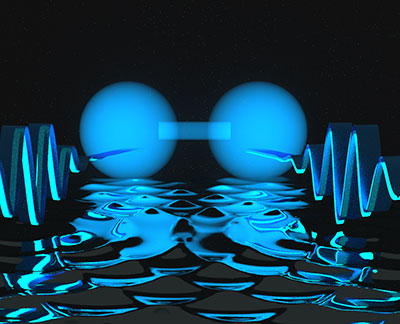
Here’s an artist’s conception of the light “molecule” provided by the researchers,

Researchers show that two photons, depicted in this artist’s conception as waves (left and right), can be locked together at a short distance. Under certain conditions, the photons can form a state resembling a two-atom molecule, represented as the blue dumbbell shape at center. Credit: E. Edwards/JQI

Researchers show that two photons, depicted in this artist’s conception as waves (left and right), can be locked together at a short distance. Under certain conditions, the photons can form a state resembling a two-atom molecule, represented as the blue dumbbell shape at center. Credit: E. Edwards/JQI

A Sept. 8, 2015 NIST news release (also available on EurekAlert*), which originated the news item, provides more information about the research (Note: Links have been removed),

The findings build on previous research that several team members contributed to before joining NIST. In 2013, collaborators from Harvard, Caltech and MIT found a way to bind two photons together so that one would sit right atop the other, superimposed as they travel. Their experimental demonstration was considered a breakthrough, because no one had ever constructed anything by combining individual photons—inspiring some to imagine that real-life lightsabers were just around the corner.

Now, in a paper forthcoming in Physical Review Letters, the NIST and University of Maryland-based team (with other collaborators) has showed theoretically that by tweaking a few parameters of the binding process, photons could travel side by side, a specific distance from each other. The arrangement is akin to the way that two hydrogen atoms sit next to each other in a hydrogen molecule.

“It’s not a molecule per se, but you can imagine it as having a similar kind of structure,” says NIST’s Alexey Gorshkov. “We’re learning how to build complex states of light that, in turn, can be built into more complex objects. This is the first time anyone has shown how to bind two photons a finite distance apart.”

While the new findings appear to be a step in the right direction—if we can build a molecule of light, why not a sword?—Gorshkov says he is not optimistic that Jedi Knights will be lining up at NIST’s gift shop anytime soon. The main reason is that binding photons requires extreme conditions difficult to produce with a roomful of lab equipment, let alone fit into a sword’s handle. Still, there are plenty of other reasons to make molecular light—humbler than lightsabers, but useful nonetheless.

“Lots of modern technologies are based on light, from communication technology to high-definition imaging,” Gorshkov says. “Many of them would be greatly improved if we could engineer interactions between photons.”

For example, engineers need a way to precisely calibrate light sensors, and Gorshkov says the findings could make it far easier to create a “standard candle” that shines a precise number of photons at a detector. Perhaps more significant to industry, binding and entangling photons could allow computers to use photons as information processors, a job that electronic switches in your computer do today.

Not only would this provide a new basis for creating computer technology, but it also could result in substantial energy savings. Phone messages and other data that currently travel as light beams through fiber optic cables has to be converted into electrons for processing—an inefficient step that wastes a great deal of electricity. If both the transport and the processing of the data could be done with photons directly, it could reduce these energy losses.

Gorshkov says it will be important to test the new theory in practice for these and other potential benefits.

“It’s a cool new way to study photons,” he says. “They’re massless and fly at the speed of light. Slowing them down and binding them may show us other things we didn’t know about them before.”

Here are links and citations for the paper. First, there’s an early version on arXiv.org and, then, there’s the peer-reviewed version, which is not yet available,

Coulomb bound states of strongly interacting photons by M. F. Maghrebi, M. J. Gullans, P. Bienias, S. Choi, I. Martin, O. Firstenberg, M. D. Lukin, H. P. Büchler, A. V. Gorshkov.      arXiv:1505.03859 [quant-ph] (or arXiv:1505.03859v1 [quant-ph] for this version)

Coulomb bound states of strongly interacting photons by M. F. Maghrebi, M. J. Gullans, P. Bienias, S. Choi, I. Martin, O. Firstenberg, M. D. Lukin, H. P. Büchler, and A. V. Gorshkov.
Phys. Rev. Lett. forthcoming in September 2015.

The first version (arXiv) is open access and I’m not sure whether or not the Physical review Letters study will be behind a paywall or be available as an open access paper.

*EurekAlert link added 10:34 am PST on Sept. 11, 2015.

A transistor based on a single silicon nanoparticle

Even after all these years, nano stuff can seem magical to me. Russian researchers according to a Sept. 8, 2015 news item on Nanotechnology Now have already developed a prototype of a transistor based on a single silicon nanoparticle,

Physicists from the Department of Nanophotonics and Metamaterials at ITMO University have experimentally demonstrated the feasibility of designing an optical analog of a transistor based on a single silicon nanoparticle. Because transistors are some of the most fundamental components of computing circuits, the results of the study have crucial importance for the development of optical computers, where transistors must be very small and ultrafast at the same time. …

A Sept. 7, 2015 ITMO University press release on EurekAlert, which originated the news item, describes the problem the researchers were grappling with and their proposed solution,

The performance of modern computers, which use electrons as signal carriers, is largely limited by the time needed to trigger the transistor – usually around 0.1 – 1 nanoseconds (1/1.000.000.000 of a second). Next-generation optical computers, however, rely on photons to carry the useful signal, which heavily increases the amount of information passing through the transistor per second. For this reason, the creation of an ultrafast and compact all-optical transistor is considered to be instrumental in the development of optical computing. Such a nanodevice would enable scientists to control the propagation of an optical signal beam by means of an external control beam within several picoseconds (1/1.000.000.000.000 of a second).

In the study, a group of Russian scientists from ITMO University, Lebedev Physical Institute and Academic University in Saint Petersburg put forward a completely new approach to design such optical transistors, having made a prototype using only one silicon nanoparticle.

The scientists found that they can dramatically change the properties of a silicon nanoparticle by irradiating it with intense and ultrashort laser pulse. The laser thus acts as a control beam, providing ultrafast photoexcitation of dense and rapidly recombining electron-hole plasma whose presence changes the dielectric permittivity of silicon for a few picoseconds. This abrupt change in the optical properties of the nanoparticle opens the possibility to control the direction, in which incident light is scattered. For instance, the direction of nanoparticle scattering can be changed from backward to forward on picoseconds timescale, depending on the intensity of the incident control laser pulse. This concept of ultrafast switching is very promising for designing of all-optical transistor.

“Generally, researchers in this field are focused on designing nanoscale all-optical transistors by means of controlling the absorption of nanoparticles, which, in essence, is entirely logical. In high absorption mode, the light signal is absorbed by the nanoparticle and cannot pass through, while out of this mode the light is allowed to propagate past the nanoparticle. However, this method did not yield any decisive results,” explains Sergey Makarov, lead author of the study and senior researcher at the Department of Nanophotonics and Metamaterials. “Our idea is different in the sense that we control not the absorption properties of the nanoparticle, but rather its scattering diagram. Let’s say, the nanoparticle normally scatters almost all incident light in the backward direction, but once we irradiate it by a control pulse, it becomes reconfigured and starts scattering light forward.”

The choice of silicon as a material for the optical transistor was not accidental. Creating an optical transistor requires the use of inexpensive materials appropriate for mass production and capable of changing their optical properties in several picoseconds (in the regime of dense electron-hole plasma) without getting overheated at the same time.

“The time it takes us to deactivate our nanoparticle amounts to just several picoseconds, while to activate it we need no more than tens of femtoseconds (1/1.000.000.000.000.000). Now we already have experimental data that clearly indicates that a single silicon nanoparticle can indeed play the role of an all-optical transistor. Currently we are planning to conduct new experiments, where, along with a laser control beam, we will introduce a useful signal beam”, concludes Pavel Belov, coauthor of the paper and head of the Department of Nanophotonics and Metamaterials.

Here’s a link to and a citation for the paper,

Tuning of Magnetic Optical Response in a Dielectric Nanoparticle by Ultrafast Photoexcitation of Dense Electron–Hole Plasma by Sergey Makarov, Sergey Kudryashov, Ivan Mukhin, Alexey Mozharov, Valentin Milichko, Alexander Krasnok, and Pavel Belov. Nano Lett., 2015, 15 (9), pp 6187–6192 DOI: 10.1021/acs.nanolett.5b02534 Publication Date (Web): August 10, 2015

Copyright © 2015 American Chemical Society

This paper is behind a paywall.

Interacting photons and quantum logic gates

University of Toronto physicists have taken the first step toward ‘working with pure light’ according to an August 25, 2015 news item on Nanotechnology Now,

A team of physicists at the University of Toronto (U of T) have taken a step toward making the essential building block of quantum computers out of pure light. Their advance, described in a paper published this week in Nature Physics, has to do with a specific part of computer circuitry known as a “logic gate.”

An August 25, 2015 University of Toronto news release by Patchen Barss, which originated the news item, provides an explanation of ‘logic gates’, photons, and the impact of this advance (Note: Links have been removed),

Logic gates perform operations on input data to create new outputs. In classical computers, logic gates take the form of diodes or transistors. But quantum computer components are made from individual atoms and subatomic particles. Information processing happens when the particles interact with one another according to the strange laws of quantum physics.

Light particles — known as “photons” — have many advantages in quantum computing, but it is notoriously difficult to get them to interact with one another in useful ways. This experiment demonstrates how to create such interactions.

“We’ve seen the effect of a single particle of light on another optical beam,” said Canadian Institute for Advanced Research (CIFAR) Senior Fellow Aephraim Steinberg, one of the paper’s authors and a researcher at U of T’s Centre for Quantum Information & Quantum Computing. “Normally light beams pass through each other with no effect at all. To build technologies like optical quantum computers, you want your beams to talk to one another. That’s never been done before using a single photon.”

The interaction was a two-step process. The researchers shot a single photon at rubidium atoms that they had cooled to a millionth of a degree above absolute zero. The photons became “entangled” with the atoms, which affected the way the rubidium interacted with a separate optical beam. The photon changes the atoms’ refractive index, which caused a tiny but measurable “phase shift” in the beam.

This process could be used as an all-optical quantum logic gate, allowing for inputs, information-processing and outputs.

“Quantum logic gates are the most obvious application of this advance,” said Steinberg. “But being able to see these interactions is the starting page of an entirely new field of optics. Most of what light does is so well understood that you wouldn’t think of it as a field of modern research. But two big exceptions are, “What happens when you deal with light one particle at a time?’ and “What happens when there are media like our cold atoms that allow different light beams to interact with each other?’”

Both questions have been studied, he says, but never together until now.

Here’s a link to and citation for the paper,

Observation of the nonlinear phase shift due to single post-selected photons by Amir Feizpour, Matin Hallaji, Greg Dmochowski, & Aephraim M. Steinberg. Nature Physics (2015) doi:10.1038/nphys3433 Published online 24 August 2015

This paper is behind a paywall.

Sea sapphires: now you see them, now you don’t and more about structural colour/color

The structural colour of the sea sapphire

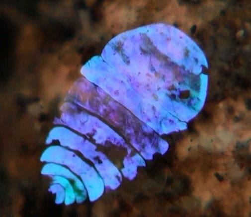
 Scientists are studying the disappearing act of this ocean-dwelling copepod. Credit: Kaj Maney, www.liquidguru.com Courtesy: American Chemical Society


Scientists are studying the disappearing act of this ocean-dwelling copepod.
Credit: Kaj Maney, www.liquidguru.com Courtesy: American Chemical Society

Now, you’ve seen a sea sapphire. Here’s more about them and the interest they hold for experts in photonics, from a July 15, 2015 news item on ScienceDaily,

Sapphirina, or sea sapphire, has been called “the most beautiful animal you’ve never seen,” and it could be one of the most magical. Some of the tiny, little-known copepods appear to flash in and out of brilliantly colored blue, violet or red existence. Now scientists are figuring out the trick to their hues and their invisibility. The findings appear in the Journal of the American Chemical Society and could inspire the next generation of optical technologies.

A July 15, 2015 American Chemical Society (ACS) news release, which originated the news item, provides more detail,

Copepods are tiny aquatic crustaceans that live in both fresh and salt water. Some males of the ocean-dwelling Sapphirina genus display striking, iridescent colors that scientists think play a role in communication and mate recognition. The shimmering animals’ colors result when light bounces off of the thin, hexagonal crystal plates that cover their backs. These plates also help them vanish, if only fleetingly. Scientists didn’t know specifically what factors contributed to creating different shades. Scientists at the Weizmann Institute [Israel] and the Interuniversity Institute for Marine Sciences in Eilat [Israel] wanted to investigate the matter.

The researchers measured the light reflectance — which determines color — of live Sapphirina males and the spacing between crystal layers. They found that changes of reflectance depended on the thickness of the spacing. And for at least one particular species, when light hits an animal at a 45-degree angle, reflectance shifts out of the visible light range and into the ultraviolet, and it practically disappears. Their results could help inform the design of artificial photonic crystal structures, which have many potential uses in reflective coatings, optical mirrors and optical displays.

To sum this up, the colour and the invisibility properties are due to thin, hexagonal crystal plates and the spacing of these plates, in other words, structural colour, which is usually achieved at the nanoscale.

Here’s a link to and a citation for the paper,

Structural Basis for the Brilliant Colors of the Sapphirinid Copepods by Dvir Gur, Ben Leshem, Maria Pierantoni, Viviana Farstey, Dan Oron, Steve Weiner, and Lia Addadi. J. Am. Chem. Soc., 2015, 137 (26), pp 8408–8411 DOI: 10.1021/jacs.5b05289 Publication Date (Web): June 22, 2015

Copyright © 2015 American Chemical Society

This paper is behind a paywall.

For anyone who’s interested, Lynn Kimlicka has a nice explanation of structural colour in a July 22, 2015 posting on the Something About Science blog where she discusses some recent research iridescence in bird feathers and synthetic melanin. She also shares a picture of her budgie and its iridescent feathers. The ‘melanin’ research was mentioned here in a May 19, 2015 posting where I also provide a link to a great 2013 piece on structural throughout the animal and plant kingdoms by Cristina Luiggi for The Scientist.

Understanding how nanostructures can affect optical properties could be leading to new ways of managing light. A July 23, 2015 news item on ScienceDaily describes a project at the University of Delaware dedicated to “changing the color of light,”

Researchers at the University of Delaware have received a $1 million grant from the W.M. Keck Foundation to explore a new idea that could improve solar cells, medical imaging and even cancer treatments. Simply put, they want to change the color of light.

A July 23, 2015 University of Delaware (UD) news release, which originated the news item, provides more information about the proposed research,

“A ray of light contains millions and millions of individual units of light called photons,” says project leader Matthew Doty. “The energy of each photon is directly related to the color of the light — a photon of red light has less energy than a photon of blue light. You can’t simply turn a red photon into a blue one, but you can combine the energy from two or more red photons to make one blue photon.”

This process, called “photon upconversion,” isn’t new, Doty says. However, the UD team’s approach to it is.

They want to design a new kind of semiconductor nanostructure that will act like a ratchet. It will absorb two red photons, one after the other, to push an electron into an excited state when it can emit a single high-energy (blue) photon.

These nanostructures will be so teeny they can only be viewed when magnified a million times under a high-powered electron microscope.

“Think of the electrons in this structure as if they were at a water park,” Doty says. “The first red photon has only enough energy to push an electron half-way up the ladder of the water slide. The second red photon pushes it the rest of the way up. Then the electron goes down the slide, releasing all of that energy in a single process, with the emission of the blue photon. The trick is to make sure the electron doesn’t slip down the ladder before the second photon arrives. The semiconductor ratchet structure is how we trap the electron in the middle of the ladder until the second photon arrives to push it the rest of the way up.”

The UD team will develop new semiconductor structures containing multiple layers of different materials, such as aluminum arsenide and gallium bismuth arsenide, each only a few nanometers thick. This “tailored landscape” will control the flow of electrons into states with varying potential energy, turning once-wasted photons into useful energy.

The UD team has shown theoretically that their semiconductors could reach an upconversion efficiency of 86 percent, which would be a vast improvement over the 36 percent efficiency demonstrated by today’s best materials. What’s more, Doty says, the amount of light absorbed and energy emitted by the structures could be customized for a variety of applications, from lightbulbs to laser-guided surgery.

How do you even begin to make structures so tiny they can only be seen with an electron microscope? In one technique the UD team will use, called molecular beam epitaxy, nanostructures will be built by depositing layers of atoms one at a time. Each structure will be tested to see how well it absorbs and emits light, and the results will be used to tailor the structure to improve performance.

The researchers also will develop a milk-like solution filled with millions of identical individual nanoparticles, each one containing multiple layers of different materials. The multiple layers of this structure, like multiple candy shells in an M&M, will implement the photon ratchet idea. Through such work, the team envisions a future upconversion “paint” that could be easily applied to solar cells, windows and other commercial products.

Improving medical tests and treatments

While the initial focus of the three-year project will be on improving solar energy harvesting, the team also will explore biomedical applications.

A number of diagnostic tests and medical treatments, ranging from CT [computed tomography] and PET [positron emission tomography] scans to chemotherapy, rely on the release of fluorescent dyes and pharmaceutical drugs. Ideally, such payloads are delivered both at specific disease sites and at specific times, but this is hard to control in practice.

The UD team aims to develop an upconversion nanoparticle that can be triggered by light to release its payload. The goal is to achieve the controlled release of drug therapies even deep within diseased human tissue while reducing the peripheral damage to normal tissue by minimizing the laser power required.

“This is high-risk, high-reward research,” Doty says. “High-risk because we don’t yet have proof-of-concept data. High-reward because it has such a huge potential impact in renewable energy to medicine. It’s amazing to think that this same technology could be used to harvest more solar energy and to treat cancer. We’re excited to get started!”

That’s it for structural colour/color today.

Capturing the particle and the wave: photographing light

On returning to school to get a bachelor’s degree, I registered in a communications course and my first paper was about science, light, and communication. The particle/wave situation still fascinates me (and I imagine many others).

A March 2, 2015 news item on phys.org describes the first successful photography of light as both particle and wave,

Light behaves both as a particle and as a wave. Since the days of Einstein, scientists have been trying to directly observe both of these aspects of light at the same time. Now, scientists at EPFL [École polytechnique fédérale de Lausanne in Switzerland] have succeeded in capturing the first-ever snapshot of this dual behavior.

Quantum mechanics tells us that light can behave simultaneously as a particle or a wave. However, there has never been an experiment able to capture both natures of light at the same time; the closest we have come is seeing either wave or particle, but always at different times. Taking a radically different experimental approach, EPFL scientists have now been able to take the first ever snapshot of light behaving both as a wave and as a particle. The breakthrough work is published in Nature Communications.

A March 2, 2015 EPFL press release (also on EurekAlert), which originated the news item, describes the science and the research,

When UV light hits a metal surface, it causes an emission of electrons. Albert Einstein explained this “photoelectric” effect by proposing that light – thought to only be a wave – is also a stream of particles. Even though a variety of experiments have successfully observed both the particle- and wave-like behaviors of light, they have never been able to observe both at the same time.

A research team led by Fabrizio Carbone at EPFL has now carried out an experiment with a clever twist: using electrons to image light. The researchers have captured, for the first time ever, a single snapshot of light behaving simultaneously as both a wave and a stream of particles particle.

The experiment is set up like this: A pulse of laser light is fired at a tiny metallic nanowire. The laser adds energy to the charged particles in the nanowire, causing them to vibrate. Light travels along this tiny wire in two possible directions, like cars on a highway. When waves traveling in opposite directions meet each other they form a new wave that looks like it is standing in place. Here, this standing wave becomes the source of light for the experiment, radiating around the nanowire.

This is where the experiment’s trick comes in: The scientists shot a stream of electrons close to the nanowire, using them to image the standing wave of light. As the electrons interacted with the confined light on the nanowire, they either sped up or slowed down. Using the ultrafast microscope to image the position where this change in speed occurred, Carbone’s team could now visualize the standing wave, which acts as a fingerprint of the wave-nature of light.

While this phenomenon shows the wave-like nature of light, it simultaneously demonstrated its particle aspect as well. As the electrons pass close to the standing wave of light, they “hit” the light’s particles, the photons. As mentioned above, this affects their speed, making them move faster or slower. This change in speed appears as an exchange of energy “packets” (quanta) between electrons and photons. The very occurrence of these energy packets shows that the light on the nanowire behaves as a particle.

“This experiment demonstrates that, for the first time ever, we can film quantum mechanics – and its paradoxical nature – directly,” says Fabrizio Carbone. In addition, the importance of this pioneering work can extend beyond fundamental science and to future technologies. As Carbone explains: “Being able to image and control quantum phenomena at the nanometer scale like this opens up a new route towards quantum computing.”

This work represents a collaboration between the Laboratory for Ultrafast Microscopy and Electron Scattering of EPFL, the Department of Physics of Trinity College (US) and the Physical and Life Sciences Directorate of the Lawrence Livermore National Laboratory. The imaging was carried out EPFL’s ultrafast energy-filtered transmission electron microscope – one of the two in the world.

For anyone who prefers videos, the EPFL researchers have  prepared a brief description (loaded with some amusing images) of their work,


Here’s a link to and a citation for the research paper,

Simultaneous observation of the quantization and the interference pattern of a plasmonic near-field by L Piazza, T.T.A. Lummen, E Quiñonez, Y Murooka, B.W. Reed, B Barwick & F Carbone. Nature Communications 6, Article number: 6407 doi:10.1038/ncomms7407 Published 02 March 2015

This is an open access paper.

Self-organizing nanotubes and nonequilibrium systems provide insights into evolution and artificial life

If you’re interested in the second law of thermodynamics, this Feb. 10, 2015 news item on ScienceDaily provides some insight into the second law, self-organized systems, and evolution,

The second law of thermodynamics tells us that all systems evolve toward a state of maximum entropy, wherein all energy is dissipated as heat, and no available energy remains to do work. Since the mid-20th century, research has pointed to an extension of the second law for nonequilibrium systems: the Maximum Entropy Production Principle (MEPP) states that a system away from equilibrium evolves in such a way as to maximize entropy production, given present constraints.

Now, physicists Alexey Bezryadin, Alfred Hubler, and Andrey Belkin from the University of Illinois at Urbana-Champaign, have demonstrated the emergence of self-organized structures that drive the evolution of a non-equilibrium system to a state of maximum entropy production. The authors suggest MEPP underlies the evolution of the artificial system’s self-organization, in the same way that it underlies the evolution of ordered systems (biological life) on Earth. …

A Feb. 10, 2015 University of Illinois College of Engineering news release (also on EurekAlert), which originated the news item, provides more detail about the theory and the research,

MEPP may have profound implications for our understanding of the evolution of biological life on Earth and of the underlying rules that govern the behavior and evolution of all nonequilibrium systems. Life emerged on Earth from the strongly nonequilibrium energy distribution created by the Sun’s hot photons striking a cooler planet. Plants evolved to capture high energy photons and produce heat, generating entropy. Then animals evolved to eat plants increasing the dissipation of heat energy and maximizing entropy production.

In their experiment, the researchers suspended a large number of carbon nanotubes in a non-conducting non-polar fluid and drove the system out of equilibrium by applying a strong electric field. Once electrically charged, the system evolved toward maximum entropy through two distinct intermediate states, with the spontaneous emergence of self-assembled conducting nanotube chains.

In the first state, the “avalanche” regime, the conductive chains aligned themselves according to the polarity of the applied voltage, allowing the system to carry current and thus to dissipate heat and produce entropy. The chains appeared to sprout appendages as nanotubes aligned themselves so as to adjoin adjacent parallel chains, effectively increasing entropy production. But frequently, this self-organization was destroyed through avalanches triggered by the heating and charging that emanates from the emerging electric current streams. (…)

“The avalanches were apparent in the changes of the electric current over time,” said Bezryadin.

“Toward the final stages of this regime, the appendages were not destroyed during the avalanches, but rather retracted until the avalanche ended, then reformed their connection. So it was obvious that the avalanches correspond to the ‘feeding cycle’ of the ‘nanotube inset’,” comments Bezryadin.

In the second relatively stable stage of evolution, the entropy production rate reached maximum or near maximum. This state is quasi-stable in that there were no destructive avalanches.

The study points to a possible classification scheme for evolutionary stages and a criterium for the point at which evolution of the system is irreversible—wherein entropy production in the self-organizing subsystem reaches its maximum possible value. Further experimentation on a larger scale is necessary to affirm these underlying principals, but if they hold true, they will prove a great advantage in predicting behavioral and evolutionary trends in nonequilibrium systems.

The authors draw an analogy between the evolution of intelligent life forms on Earth and the emergence of the wiggling bugs in their experiment. The researchers note that further quantitative studies are needed to round out this comparison. In particular, they would need to demonstrate that their “wiggling bugs” can multiply, which would require the experiment be reproduced on a significantly larger scale.

Such a study, if successful, would have implications for the eventual development of technologies that feature self-organized artificial intelligence, an idea explored elsewhere by co-author Alfred Hubler, funded by the Defense Advanced Research Projects Agency [DARPA]. [emphasis mine]

“The general trend of the evolution of biological systems seems to be this: more advanced life forms tend to dissipate more energy by broadening their access to various forms of stored energy,” Bezryadin proposes. “Thus a common underlying principle can be suggested between our self-organized clouds of nanotubes, which generate more and more heat by reducing their electrical resistance and thus allow more current to flow, and the biological systems which look for new means to find food, either through biological adaptation or by inventing more technologies.

“Extended sources of food allow biological forms to further grow, multiply, consume more food and thus produce more heat and generate entropy. It seems reasonable to say that real life organisms are still far from the absolute maximum of the entropy production rate. In both cases, there are ‘avalanches’ or ‘extinction events’, which set back this evolution. Only if all free energy given by the Sun is consumed, by building a Dyson sphere for example, and converted into heat then a definitely stable phase of the evolution can be expected.”

“Intelligence, as far as we know, is inseparable from life,” he adds. “Thus, to achieve artificial life or artificial intelligence, our recommendation would be to study systems which are far from equilibrium, with many degrees of freedom—many building blocks—so that they can self-organize and participate in some evolution. The entropy production criterium appears to be the guiding principle of the evolution efficiency.”

I am fascinated

  • (a) because this piece took an unexpected turn onto the topic of artificial life/artificial intelligence,
  • (b) because of my longstanding interest in artificial life/artificial intelligence,
  • (c) because of the military connection, and
  • (d) because this is the first time I’ve come across something that provides a bridge from fundamental particles to nanoparticles.

Here’s a link to and a citation for the paper,

Self-Assembled Wiggling Nano-Structures and the Principle of Maximum Entropy Production by A. Belkin, A. Hubler, & A. Bezryadin. Scientific Reports 5, Article number: 8323 doi:10.1038/srep08323 Published 09 February 2015

Adding to my delight, this paper is open access.