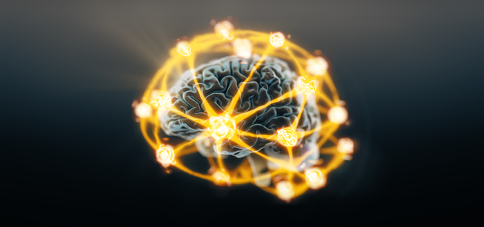
A March 8, 2023 news item on phys.org announces research from Swiss and Italian researchers into a new type of memristor,
Researchers at Empa, ETH Zurich and the Politecnico di Milano are developing a new type of computer component that is more powerful and easier to manufacture than its predecessors. Inspired by the human brain, it is designed to process large amounts of data fast and in an energy-efficient way.
In many respects, the human brain is still superior to modern computers. Although most people can’t do math as fast as a computer, we can effortlessly process complex sensory information and learn from experiences, while a computer cannot – at least not yet. And, the brain does all this by consuming less than half as much energy as a laptop.
One of the reasons for the brain’s energy efficiency is its structure. The individual brain cells – the neurons and their connections, the synapses – can both store and process information. In computers, however, the memory is separate from the processor, and data must be transported back and forth between these two components. The speed of this transfer is limited, which can slow down the whole computer when working with large amounts of data.
One possible solution to this bottleneck are novel computer architectures that are modeled on the human brain. To this end, scientists are developing so-called memristors: components that, like brain cells, combine data storage and processing. A team of researchers from Empa, ETH Zurich and the “Politecnico di Milano” has now developed a memristor that is more powerful and easier to manufacture than its predecessors. The researchers have recently published their results in the journal Science Advances.
Performance through mixed ionic and electronic conductivity
The novel memristors are based on halide perovskite nanocrystals, a semiconductor material known from solar cell manufacturing. “Halide perovskites conduct both ions and electrons,” explains Rohit John, former ETH Fellow and postdoctoral researcher at both ETH Zurich and Empa. “This dual conductivity enables more complex calculations that closely resemble processes in the brain.”
The researchers conducted the experimental part of the study entirely at Empa: They manufactured the thin-film memristors at the Thin Films and Photovoltaics laboratory and investigated their physical properties at the Transport at Nanoscale Interfaces laboratory. Based on the measurement results, they then simulated a complex computational task that corresponds to a learning process in the visual cortex in the brain. The task involved determining the orientation of light based on signals from the retina.
“As far as we know, this is only the second time this kind of computation has been performed on memristors,” says Maksym Kovalenko, professor at ETH Zurich and head of the Functional Inorganic Materials research group at Empa. “At the same time, our memristors are much easier to manufacture than before.” This is because, in contrast to many other semiconductors, perovskites crystallize at low temperatures. In addition, the new memristors do not require the complex preconditioning through application of specific voltages that comparable devices need for such computing tasks. This makes them faster and more energy-efficient.
Complementing rather than replacing
The technology, though, is not quite ready for deployment yet. The ease with which the new memristors can be manufactured also makes them difficult to integrate with existing computer chips: Perovskites cannot withstand temperatures of 400 to 500 degrees Celsius that are needed to process silicon – at least not yet. But according to Daniele Ielmini, professor at the “Politecnico di Milano”, that integration is key to the success for new brain-like computer technologies. “Our goal is not to replace classical computer architecture,” he explains. “Rather, we want to develop alternative architectures that can perform certain tasks faster and with greater energy efficiency. This includes, for example, the parallel processing of large amounts of data, which is generated everywhere today, from agriculture to space exploration.”
Promisingly, there are other materials with similar properties that could be used to make high-performance memristors. “We can now test our memristor design with different materials,” says Alessandro Milozzi, a doctoral student at the “Politecnico di Milano”. “It is quite possible that some of them are better suited for integration with silicon.”
The SupraBioNano Lab (SBNLab) at the Politecnico di Milano’s Department of Chemistry, Materials and Chemical Engineering “Giulio Natta”, in partnership with the University of Bologna and the Aalto University of Helsinki (Finland) has, for the first time, synthesised a superfluorinated gold nanocluster, made up of a core of only 25 gold atoms, to which 18 branch-structured fluorinated molecules are linked.
The metal clusters are an innovative class of very complex nanomaterial, characterised by ultra-small dimensions (<2nm) and peculiar chemical-physical properties such as luminescence and catalytic activity, which encourage its application in various scientific fields of high importance in relation to modern global challenges. These include precision medicine, in which metal nanoclusters are used as innovative probes for diagnostic and therapeutic applications, and the energy transition, where they are applied as efficient catalysers for the production of green hydrogen.
The crystallisation of metal nanoclusters offers the possibility of obtaining high-purity samples, allowing their fine atomic structure to be determined; however, at present this remains a very difficult process to control. The methodologies developed in this study promoted the crystallisation of nanoclusters, allowing their atomic structure to be determined. The end result is the structural description of the most complex fluorinated nano-object ever reported.
The atomic structure has been determined by means of x-ray diffraction at the Sincrotrone Elettra in Trieste. It will soon be possible to study the structure of these advanced nanomaterials at the Politecnico di Milano, where – thanks also to the grant from the Region of Lombardy – Next-GAME (Next-Generation Advanced Materials), a laboratory dedicated to the use of state-of-the-art x-ray instruments to characterise crystals, nanoparticles and colloids, is being established.
Among the authors of the study were Prof. Pierangelo Metrangolo, Prof. Giancarlo Terraneo, Prof. Valentina Dichiarante, Prof. Francesca Baldelli Bombelli, Dr. Claudia Pigliacelli (SBNLab); professor Giulio Cerullo, from the Politecnico di Milano’s Department of Physics, also contributed to the study, looking at the nanocluster’s optical characteristics and demonstrating the fluorinated binders’ impact on the gold core’s optical activity.
Here’s a link to and a citation for the paper,
High-resolution crystal structure of a 20 kDa superfluorinated gold nanocluster by Claudia Pigliacelli, Angela Acocella, Isabel Díez, Luca Moretti, Valentina Dichiarante, Nicola Demitri, Hua Jiang, Margherita Maiuri, Robin H. A. Ras, Francesca Baldelli Bombelli, Giulio Cerullo, Francesco Zerbetto, Pierangelo Metrangolo & Giancarlo Terraneo. Nature Communications volume 13, Article number: 2607 (2022) DOI https://doi.org/10.1038/s41467-022-29966-2 Published11 May 2022 DOI https://doi.org/10.1038/s41467-022-29966-2
This March 24, 2022 news item on Nanowerk announcing work on a quantum memristor seems to have had a rough translation from German to English,
In recent years, artificial intelligence has become ubiquitous, with applications such as speech interpretation, image recognition, medical diagnosis, and many more. At the same time, quantum technology has been proven capable of computational power well beyond the reach of even the world’s largest supercomputer.
Physicists at the University of Vienna have now demonstrated a new device, called quantum memristor, which may allow to combine these two worlds, thus unlocking unprecedented capabilities. The experiment, carried out in collaboration with the National Research Council (CNR) and the Politecnico di Milano in Italy, has been realized on an integrated quantum processor operating on single photons.
At the heart of all artificial intelligence applications are mathematical models called neural networks. These models are inspired by the biological structure of the human brain, made of interconnected nodes. Just like our brain learns by constantly rearranging the connections between neurons, neural networks can be mathematically trained by tuning their internal structure until they become capable of human-level tasks: recognizing our face, interpreting medical images for diagnosis, even driving our cars. Having integrated devices capable of performing the computations involved in neural networks quickly and efficiently has thus become a major research focus, both academic and industrial.
One of the major game changers in the field was the discovery of the memristor, made in 2008. This device changes its resistance depending on a memory of the past current, hence the name memory-resistor, or memristor. Immediately after its discovery, scientists realized that (among many other applications) the peculiar behavior of memristors was surprisingly similar to that of neural synapses. The memristor has thus become a fundamental building block of neuromorphic architectures.
A group of experimental physicists from the University of Vienna, the National Research Council (CNR) and the Politecnico di Milano led by Prof. Philip Walther and Dr. Roberto Osellame, have now demonstrated that it is possible to engineer a device that has the same behavior as a memristor, while acting on quantum states and being able to encode and transmit quantum information. In other words, a quantum memristor. Realizing such device is challenging because the dynamics of a memristor tends to contradict the typical quantum behavior.
By using single photons, i.e. single quantum particles of lights, and exploiting their unique ability to propagate simultaneously in a superposition of two or more paths, the physicists have overcome the challenge. In their experiment, single photons propagate along waveguides laser-written on a glass substrate and are guided on a superposition of several paths. One of these paths is used to measure the flux of photons going through the device and this quantity, through a complex electronic feedback scheme, modulates the transmission on the other output, thus achieving the desired memristive behavior. Besides demonstrating the quantum memristor, the researchers have provided simulations showing that optical networks with quantum memristor can be used to learn on both classical and quantum tasks, hinting at the fact that the quantum memristor may be the missing link between artificial intelligence and quantum computing.
“Unlocking the full potential of quantum resources within artificial intelligence is one of the greatest challenges of the current research in quantum physics and computer science”, says Michele Spagnolo, who is first author of the publication in the journal “Nature Photonics”. The group of Philip Walther of the University of Vienna has also recently demonstrated that robots can learn faster when using quantum resources and borrowing schemes from quantum computation. This new achievement represents one more step towards a future where quantum artificial intelligence become reality.
Here’s a link to and a citation for the paper,
Experimental photonic quantum memristor by Michele Spagnolo, Joshua Morris, Simone Piacentini, Michael Antesberger, Francesco Massa, Andrea Crespi, Francesco Ceccarelli, Roberto Osellame & Philip Walther. Nature Photonics volume 16, pages 318–323 (2022) DOI: https://doi.org/10.1038/s41566-022-00973-5 Published 24 March 2022 Issue Date April 2022
First off, there’s Canada’s annual Science Odyssey (see my April 26, 2021 posting for more about the government initiative or you can go directly to the Science Odyssey website for a listing of the events).
Since posting about Science Odyssey, I have received a number of emails announcing event and not all of them are part of the Odyssey experience.
From the looks of things, May 2021 is going to be a very busy month. Given how early it is in the month I expect to receive another batch of notices and most likely will post another May 2021 events roundup.
At this point, there’s a heavy emphasis on architecture (human and other) and design.
Proximal Spaces on May 3, 2021
This is one of those event within an event notices. There’s a festival: FACTT 20/21 – Improbable Times. Trans-disciplinary & Trans-national Festival of Art & Science in Portugal and within the festival there is Proximal Spaces in Toronto, Canada. Here’s more from the ArtScience Salon (ArtSci Salon) May 1, 2021 announcement (received via email),
Proximal Spaces
May 3, 2021 – 3.00 PM (EST) [12 pm PST]
Join us at this poetry reading by six Canadian artists responding to the work of eight bioartists. Event with be streamed on Facebook Live.
Please note that you don’t need to sign up in order to access the streaming as it is public.
Proximal Spaces’ is a multi-modal exhibition that explores the environment at multiple scales in concentric circles of proximity to the body. Inspired by Edward Hall’s [Edward Twitchell Hall or E. T. Hall] 1961 notation of intimate (1.5ft), personal (4ft), social (12ft) and public (25ft) spaces in his “Proxemics” diagrams, the installation portion presents similar diagrams of his concentric circles affixed to the wall of the gallery space, as well as developed in Augmented Reality around the venue. Each of these diagrams is a montage of microscopic and sub-microscopic images of the everyday environment as experienced by a collaborative team of international bioartists, and arrayed in a fractal form. In addition, an AR-enabled application explores the invisible environments of computer generated bioaerosols suspended in the air of virtual space.
This work visualizes the variegated response of the biological environment to unprecedented levels of physical distancing and self-isolation and recent developments in vaccine design that impact our understanding of interpersonal and interspecies ‘messaging’. What continues to thrive in the 6ft ‘dead spaces’ between us? What invisible particles linger on and create a biological archive through our movements through space? The artwork presents an interesting mode of interspecies engagement through hybrid virtual and physical interaction.
In the spring of 2021, six Canadian poets – Kelley Aitken, nancy viva davis halifax, Maureen Hynes, Anita Lahey, Dilys Leman, & Sheila Stewart – came together to pursue a lyric response to Proximal Spaces. They were challenged and inspired by the virtual exhibition with its combination of art, science, and proxemics. The focus of the artworks – what inhabits and thrives in the spaces and environments where we live, work, and breathe—generated six distinctive poems.
Poets: Kelley Aitken, nancy viva davis halifax, Maureen Hynes, Anita Lahey, Dilys Leman, & Sheila Stewart
Bioartists: Roberta Buiani, Nathalie Dubois Calero, Sarah Choukah, Nicole Clouston, Jess Holtz, Mick Lorusso, Maro Pebo, Felipe Shibuya
This project is part of FACTT-Improbable Times (http://factt.arteinstitute.org/), a project spearheaded and promoted by the Arte Institute we are in or production and conception partners with Cultivamos Cultura and Ectopia (Portugal), InArts Lab@Ionian University (Greece), ArtSci Salon@The Fields Institute and Sensorium@York University (Canada), School of Visual Arts (USA), UNAM [National Autonomous University of Mexico], Arte+Ciência and Bioscénica (Mexico), and Central Academy of Fine Arts (China). Together we will work and bring into being our ideas and actions for this during the year of 2021!
Morphogenesis: Geometry, Physics, and Biology on May 5, 2021
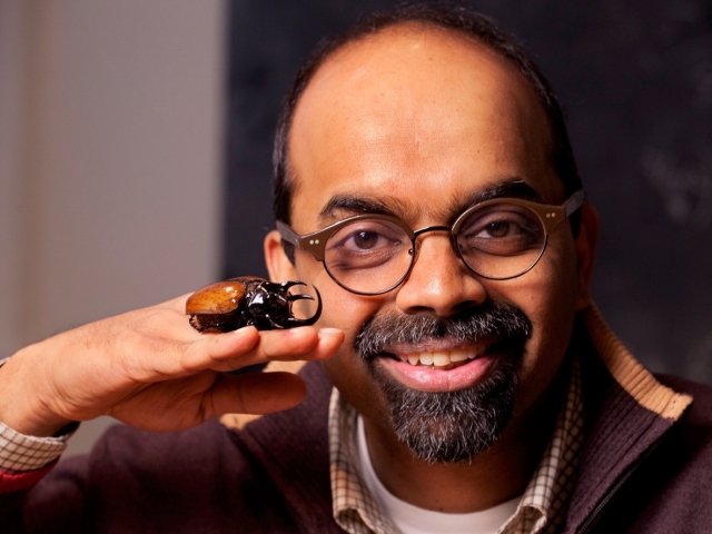
i love this image, he seems so delighted to show off the bug (?),
Harvard professor L. Mahadevan
Here’s more from the Perimeter Institute for Theoretical Physics (PI) April 30, 2021 announcement (received via email),
Earth is home to millions of different species – from simple plants and unicellular organisms to trees and whales and humans. The incredible diversity of life on Earth led Charles Darwin to lament that it is “enough to drive the sanest man mad.”
How can we make sense of this diversity of form, which arises from the process of morphogenesis that links molecular- and cellular-level processes to conspire and lead to the emergence of “endless forms most beautiful,” as Darwin said?
In his May 5 [2021] lecture webcast, Harvard professor L. Mahadevan [Lakshminarayanan Mahadevan] will take viewers on a journey into the mathematical, physical, and biological workings of morphogenesis to demonstrate how scientists are beginning to unlock many of the secrets that have vexed scientists since Darwin.
Possible Worlds: “How Will We Live Together?” on May 6, 2021
For those who are interested in human architecture, there’s this from a May 3, 3021 Berggruen institute announcement (received via email) about a talk by Chilean architect and 2016 Pritzker Prize winner, Alejandro Gastón Aravena Mori (Alejandro Aravena),
Possible Worlds: How Will We Live Together
May 6, 2021
11am — Virtual
Possible Worlds: The UCLA [University of California at Los Angeles] – Berggruen Institute Speaker Series is a new partnership between the UCLA Division of Humanities and the Berggruen Institute.
Please click here to submit a question to Alejandro Aravena
About Alejandro Aravena Alejandro Aravena is an architect, founder and executive director of the firm Elemental. His works include the “Siamese Towers” at the Catholic University of Chile and the Novartis office campus in Shanghai. In 2016, the New York Times named Aravena one of the world’s “creative geniuses” who had helped define culture. He and Elemental have received numerous honors, including the 2016 Pritzker Architecture Prize, the 2015 London Design Museum’s Design of the Year award and the 2011 Index Award. Aravena currently serves as the president of the Pritzker Prize jury. Aravena’s lecture title, “How Will We Live Together?” echoes the theme of the upcoming international architecture exhibition, Biennale Architettura, in which Elemental will be participating.
Featuring a discussion with moderator Dana Cuff
Dana Cuff is Professor of Architecture and Urban Design at UCLA, where she is also Director of cityLAB, an award-winning think tank that advances goals of spatial justice through experimental urbanism and architecture (www.cityLAB.aud.ucla.edu). Since receiving her Ph.D. in Architecture from Berkeley, Cuff has published and lectured widely about affordable housing, the architectural profession, and Los Angeles’ urban history. She is author of several books, including The Provisional City about postwar housing in L.A., and a co-authored book called Urban Humanities: New Practices for Reimagining the City, documenting her collaborative, crossdisciplinary research and teaching at UCLA funded by the Mellon Foundation. Based on cityLAB’s design research, Cuff co-authored landmark legislation that permits “backyard homes” on some 8.1 million single-family properties, doubling the density of suburbs across California (AB 2299, Bloom-2016). In 2019, cityLAB opened a satellite center in the MacArthur Park/Westlake neighborhood where a deep, multi-year exchange with community organizations is already demonstrating ways that humanistic design of the public realm can create more compassionate cities. Cuff recently received three awards that describe her career: Women in Architecture Activist of the Year (2019, Architectural Record); Distinguished Leadership in Architectural Research (2020, ARCC); and Educator of the Year (2021, American Institute of Architects Los Angeles).
About the Series Possible Worlds: The UCLA – Berggruen Institute Speaker Series is a new partnership between the UCLA Division of Humanities and the Berggruen Institute. This semiannual series will bring some of today’s most imaginative intellectual leaders and creators to deliver public talks on the future of humanity. Through the lens of their singular achievements and experiences, these trailblazers in creativity, innovation, philosophy and politics will lecture on provocative topics that explore current challenges and transformations in human progress.
UCLA faculty and students have long been at the forefront of interpreting the world’s legacy of language, literature, art and science. UCLA Humanities serves a vital role in readying future leaders to articulate their thoughts with clarity and imagination, to interpret the world of ideas, and to live as informed citizens in an increasingly complex world. We are proud to be partnering in this lecture series with the Berggruen Institute, whose work addresses the “Great Transformations” taking place in technology and culture, politics and economics, global power arrangements, and even how we perceive ourselves as humans. The Institute seeks to connect deep thought in the human sciences — philosophy and culture — to the pursuit of practical improvements in governance.
A selection committee comprising representatives of UCLA and the Berggruen Institute has been formed to make recommendations for lecturers. The committee includes:
• Ursula Heise, Professor and Chair, Department of English; Professor, UCLA Institute of the Environment and Sustainability; Marcia H. Howard Term Chair in Literary Studies • Pamela Hieronymi, Professor of Philosophy • Anastasia Loukaitou-Sideris, Professor of Urban Planning; Associate Provost for Academic Planning • Todd Presner, Associate Dean, Digital Initiatives; Chair of the Digital Humanities Program; Michael and Irene Ross Endowed Chair of Yiddish Studies; Professor of Germanic Languages and Comparative Literature • Lynn Vavreck, Professor, Department of Political Science; Marvin Hoffenberg Professor of American Politics and Public Policy • David Schaberg, Senior Dean of the UCLA College; Dean of Humanities; Professor, Asian Languages & Cultures • Nils Gilman, Vice President of Programs, the Berggruen Institute
Generative Art and Computational Creativity starts May 7, 2021
A Spring 2021 MetaCreation Lab (Simon Fraser University; SFU) newsletter (received via email on April 23, 2021) highlights a number of festival submissions and papers along with some news about a free introductory course. First, the video introduction to the course,
This first course in the two-part program, Generative Art and Computational Creativity [there’s a fee for part two], proposes an introduction and overview of the history and practice of generative arts and computational creativity with an emphasis on the formal paradigms and algorithms used for generation. The full program will be taught by Associate Professor from the School of Interactive Arts and Technology at Simon Fraser University and multi-disciplinary researcher, Philippe Pasquier.
On the technical side, we will study core techniques from mathematics, artificial intelligence, and artificial life that are used by artists, designers and musicians across the creative industry. We will start with processes involving chance operations, chaos theory and fractals and move on to see how stochastic processes, and rule-based approaches can be used to explore creative spaces. We will study agents and multi-agent systems and delve into cellular automata, and virtual ecosystems to explore their potential to create novel and valuable artifacts and aesthetic experiences.
The presentation is illustrated by numerous examples from past and current productions across creative practices such as visual art, new media, music, poetry, literature, performing arts, design, architecture, games, robot-art, bio-art and net-art. Students get to practice these algorithms first hand and develop new generative pieces through assignments and projects in MAX. Finally, the course addresses relevant philosophical, and societal debates associated with the automation of creative tasks.
Music for this course was composed with the StyleMachineLite Max for Live engine of Metacreative Inc.
Artistic direction: Philippe Pasquier, Programmation: Arne Eigenfeldt, Sound Production: Philippe Bertrand
Schedule
This course is in adaptive mode and is open for enrollment. Learn more about adaptive courses here.
Session 1: Introduction and Typology of Generative Art (May 7, 2021) To start off this course, we define generative art and computational creativity and discuss how these relate through the study of prominent examples. We establish a typology of generative systems based on levels of autonomy and agency.
Session 2: History Of Generative Art, Chance Operations, and Chaos Theory (May 14, 2021) Generative art is nothing new, and this session goes through the history of the field from pre-history to the popularization of computers. We study chance, noise, fractals, chaos theory, and their applications in visual art and music.
Session 3: Rule-Based Systems, Grammars and Markov Chains (May 21, 2021) This session introduces and illustrate the generative potential of rule-based and expert systems. We study generative grammars through the Chomsky hierarchy, and introduce L-systems, shape grammars, and Markov chains. We discuss how these have been applied in visual art, music, design, architecture, and electronic literature.
Session 4: Cognitive Agents And Multiagent Systems (May 28, 2021) This session introduces the concepts underlying the notion of artificial agents. We study the belief, desire, and intention (BDI) cognitive architecture, and message based agent communication resting on the speech act theory. We discuss musical agents, conversational agents, chat bots and twitter bots and their artistic potential.
Session 5: Reactive Agents And Multiagent Systems (June 4, 2021) In this session, we introduce reactive agents and the subsumption architecture. We study boids, and detail how complex behaviors can emerge from a distributed population of simple artificial agents. We look at a myriad of applications from ant painting to swarm music and we discuss artistic approaches to virtual ecosystems.
Session 6: A-Life And Cellular Automaton (June 11, 2021) In this concluding session, we introduce artificial life (A-life). We study cellular automaton, multi-agent ecosystems for music, visual art, non-photorealistic rendering, and gaming. The session also concludes the class by reflecting on the state of the art in the field and its consequences on creative practices.
If you’re interested in the lab and its other projects, go to metacreationlab.net.
Architectural Portraits on May 13, 2021
From the May 2021 Dante Alighieri Society of British Columbia’s newsletter,
ARCHITECTURAL PORTRAITS: EXPLORING THE RELATIONSHIP BETWEEN BODY, DESIGN & THE BUILT ENVIRONMENT A talk by architect & photographer Oliviero Godi (Politecnico di Milano)
Photo by Oliviero Godi – Frantoio Ipogeo nel Salento
THURSDAY, May 13, 2021 IN ENGLISH – ON ZOOM at 5:00 pm (PST)
Admission:
FREE for the Dante Society’s members
$5 MINIMUM DONATION for non-members
Become a member! Annual membership $30.00 – See membership benefits here
The human being – so fragile, so ethereal, speaking a sweet language. A piece of architecture – so physically imminent, so solid, speaking a language of hardness.
Photo by Oliviero Godi – Frantoio Ipogeo nel Salento
Join photographer & architect Oliviero Godi as he explores the relationship between the body & the material, the transient & the permanent, in search of the correct balance where neither element prevails.
To make your donation, please send an e-transfer to info@dantesocietybc.ca. Thank you!
Learn More [about this other upcoming Cultural Events]
Respiration and the Brain on May 25, 2021
Before getting to the April 29, 2021 BrainTalks announcement, here’s a little bit about BrainTalks from their webspace on the University of British Columbia (UBC) website,
BrainTalks is a series of talks inviting you to contemplate emerging research about the brain. Researchers studying the brain, from various disciplines including psychiatry, neuroscience, neuroimaging, and neurology, gather to discuss current leading edge topics on the mind.
As an audience member, you join the discussion at the end of the talk, both in the presence of the entire audience, and with an opportunity afterwards to talk with the speaker more informally in a catered networking session. The talks also serve as a connecting place for those interested in similar topics, potentially launching new endeavours or simply connecting people in discussions on how to approach their research, their knowledge, or their clinical practice.
For the general public, these talks serve as a channel where by knowledge usually sequestered in inaccessible journals or university classrooms, is now available, potentially allowing people to better understand their brains and minds, how they work, and how to optimize brain health.
[UBC School of Medicine Department of Psychiatry]
Onto the April 29, 2021 BrainTalks announcement (received via email),
BrainTalks: Respiration and the Brain
Tuesday, May 25th, 2021 from 6:00 PM – 7:30 PM [PT]
Join us for a series of online talks exploring questions of respiration and the brain. Emerging empirical research will be presented on ventilation-associated brain injury and breathing-based interventions for the treatment of stress and anxiety disorders. We presenters will include Dr. Thiago Bassi, Dr. Lloyd Lalande and Taylor Willi, MSc.
Dr. Thiago Bassi will address the biological connection between the brain and lungs, exploring the potential adverse effects of mechanical ventilation on the brain. Dr. Bassi is a neurosurgeon and neuroscientist, who worked clinically for more than ten years in Brazil. He joined the Lungpacer Medical team and C2B2 lab in 2017, and is currently completing his doctorate in Biomedicine Physiology at Simon Fraser University.
Dr. Lloyd Lalande will describe Guided Respiration Mindfulness Therapy (GRMT), as an emerging clinical breathwork intervention for its effectiveness in reducing depression, anxiety and stress, and in increasing mindfulness and sense of wellbeing. Dr. Lalonde is an Assistant Professor teaching psychology at the Buddhist TzuChi University of Science and Technology, and the developer of GRMT. His current research is based out of the TzuChi Buddhist General Hospital, investigating GRMT as an evidence-based treatment for a variety of outcomes.
Mr. Taylor Willi will present the findings of his dissertation research comparing the effect of performing daily brief relaxation techniques on measures of stress and anxiety. Mr. Willi completed a Masters Degree of Neuroscience at the University of British Columbia, and is currently completing his doctorate in Clinical Psychology at Simon Fraser University.
Each of the speakers will present an overview of their research findings investigating respiration in three unique ways. Following their presentations, the speakers will be available for an audience-drive panel discussion.
They don’t mention COVID-19 but given that seriously ill patients with the disease are routinely placed on ventilators, it is almost certainly going to be mentioned in the presentations.