Tag Archives: Purdue University

AI (artificial intelligence) and a hummingbird robot

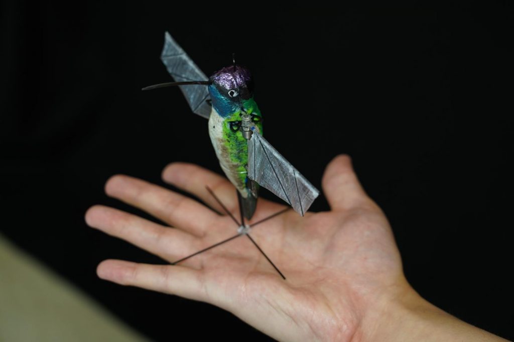
Every once in a while I stumble across a hummingbird robot story (my August 12, 2011 posting and my August 1, 2014 posting). Here’s what the hummingbird robot looks like now (hint: there’s a significant reduction in size),

Caption: Purdue University researchers are building robotic hummingbirds that learn from computer simulations how to fly like a real hummingbird does. The robot is encased in a decorative shell. Credit: Purdue University photo/Jared Pike

I think this is the first time I’ve seen one of these projects not being funded by the military, which explains why the researchers are more interested in using these hummingbird robots for observing wildlife and for rescue efforts in emergency situations. Still, they do acknowledge theses robots could also be used in covert operations.

From a May 9, 2019 news item on ScienceDaily,

What can fly like a bird and hover like an insect?

Your friendly neighborhood hummingbirds. If drones had this combo, they would be able to maneuver better through collapsed buildings and other cluttered spaces to find trapped victims.

Purdue University researchers have engineered flying robots that behave like hummingbirds, trained by machine learning algorithms based on various techniques the bird uses naturally every day.

This means that after learning from a simulation, the robot “knows” how to move around on its own like a hummingbird would, such as discerning when to perform an escape maneuver.

Artificial intelligence, combined with flexible flapping wings, also allows the robot to teach itself new tricks. Even though the robot can’t see yet, for example, it senses by touching surfaces. Each touch alters an electrical current, which the researchers realized they could track.

“The robot can essentially create a map without seeing its surroundings. This could be helpful in a situation when the robot might be searching for victims in a dark place — and it means one less sensor to add when we do give the robot the ability to see,” said Xinyan Deng, an associate professor of mechanical engineering at Purdue.

The researchers even have a video,

A May 9, 2019 Purdue University news release (also on EurekAlert), which originated the news item, provides more detail,


The researchers [presented] their work on May 20 at the 2019 IEEE International Conference on Robotics and Automation in Montreal. A YouTube video is available at https://www.youtube.com/watch?v=hl892dHqfA&feature=youtu.be. [it’s the video I’ve embedded in the above]

Drones can’t be made infinitely smaller, due to the way conventional aerodynamics work. They wouldn’t be able to generate enough lift to support their weight.

But hummingbirds don’t use conventional aerodynamics – and their wings are resilient. “The physics is simply different; the aerodynamics is inherently unsteady, with high angles of attack and high lift. This makes it possible for smaller, flying animals to exist, and also possible for us to scale down flapping wing robots,” Deng said.

Researchers have been trying for years to decode hummingbird flight so that robots can fly where larger aircraft can’t. In 2011, the company AeroVironment, commissioned by DARPA, an agency within the U.S. Department of Defense, built a robotic hummingbird that was heavier than a real one but not as fast, with helicopter-like flight controls and limited maneuverability. It required a human to be behind a remote control at all times.

Deng’s group and her collaborators studied hummingbirds themselves for multiple summers in Montana. They documented key hummingbird maneuvers, such as making a rapid 180-degree turn, and translated them to computer algorithms that the robot could learn from when hooked up to a simulation.

Further study on the physics of insects and hummingbirds allowed Purdue researchers to build robots smaller than hummingbirds – and even as small as insects – without compromising the way they fly. The smaller the size, the greater the wing flapping frequency, and the more efficiently they fly, Deng says.

The robots have 3D-printed bodies, wings made of carbon fiber and laser-cut membranes. The researchers have built one hummingbird robot weighing 12 grams – the weight of the average adult Magnificent Hummingbird – and another insect-sized robot weighing 1 gram. The hummingbird robot can lift more than its own weight, up to 27 grams.

Designing their robots with higher lift gives the researchers more wiggle room to eventually add a battery and sensing technology, such as a camera or GPS. Currently, the robot needs to be tethered to an energy source while it flies – but that won’t be for much longer, the researchers say.

The robots could fly silently just as a real hummingbird does, making them more ideal for covert operations. And they stay steady through turbulence, which the researchers demonstrated by testing the dynamically scaled wings in an oil tank.

The robot requires only two motors and can control each wing independently of the other, which is how flying animals perform highly agile maneuvers in nature.

“An actual hummingbird has multiple groups of muscles to do power and steering strokes, but a robot should be as light as possible, so that you have maximum performance on minimal weight,” Deng said.

Robotic hummingbirds wouldn’t only help with search-and-rescue missions, but also allow biologists to more reliably study hummingbirds in their natural environment through the senses of a realistic robot.

“We learned from biology to build the robot, and now biological discoveries can happen with extra help from robots,” Deng said.
Simulations of the technology are available open-source at https://github.com/
purdue-biorobotics/flappy
.

Early stages of the work, including the Montana hummingbird experiments in collaboration with Bret Tobalske’s group at the University of Montana, were financially supported by the National Science Foundation.

The researchers have three paper on arxiv.org for open access peer review,

Learning Extreme Hummingbird Maneuvers on Flapping Wing Robots
Fan Fei, Zhan Tu, Jian Zhang, and Xinyan Deng
Purdue University, West Lafayette, IN, USA
https://arxiv.org/abs/1902.0962

Biological studies show that hummingbirds can perform extreme aerobatic maneuvers during fast escape. Given a sudden looming visual stimulus at hover, a hummingbird initiates a fast backward translation coupled with a 180-degree yaw turn, which is followed by instant posture stabilization in just under 10 wingbeats. Consider the wingbeat frequency of 40Hz, this aggressive maneuver is carried out in just 0.2 seconds. Inspired by the hummingbirds’ near-maximal performance during such extreme maneuvers, we developed a flight control strategy and experimentally demonstrated that such maneuverability can be achieved by an at-scale 12- gram hummingbird robot equipped with just two actuators. The proposed hybrid control policy combines model-based nonlinear control with model-free reinforcement learning. We use model-based nonlinear control for nominal flight control, as the dynamic model is relatively accurate for these conditions. However, during extreme maneuver, the modeling error becomes unmanageable. A model-free reinforcement learning policy trained in simulation was optimized to ‘destabilize’ the system and maximize the performance during maneuvering. The hybrid policy manifests a maneuver that is close to that observed in hummingbirds. Direct simulation-to-real transfer is achieved, demonstrating the hummingbird-like fast evasive maneuvers on the at-scale hummingbird robot.

Acting is Seeing: Navigating Tight Space Using Flapping Wings
Zhan Tu, Fan Fei, Jian Zhang, and Xinyan Deng
Purdue University, West Lafayette, IN, USA
https://arxiv.org/abs/1902.0868

Wings of flying animals can not only generate lift and control torques but also can sense their surroundings. Such dual functions of sensing and actuation coupled in one element are particularly useful for small sized bio-inspired robotic flyers, whose weight, size, and power are under stringent constraint. In this work, we present the first flapping-wing robot using its flapping wings for environmental perception and navigation in tight space, without the need for any visual feedback. As the test platform, we introduce the Purdue Hummingbird, a flapping-wing robot with 17cm wingspan and 12 grams weight, with a pair of 30-40Hz flapping wings driven by only two actuators. By interpreting the wing loading feedback and its variations, the vehicle can detect the presence of environmental changes such as grounds, walls, stairs, obstacles and wind gust. The instantaneous wing loading can be obtained through the measurements and interpretation of the current feedback by the motors that actuate the wings. The effectiveness of the proposed approach is experimentally demonstrated on several challenging flight tasks without vision: terrain following, wall following and going through a narrow corridor. To ensure flight stability, a robust controller was designed for handling unforeseen disturbances during the flight. Sensing and navigating one’s environment through actuator loading is a promising method for mobile robots, and it can serve as an alternative or complementary method to visual perception.

Flappy Hummingbird: An Open Source Dynamic Simulation of Flapping Wing Robots and Animals
Fan Fei, Zhan Tu, Yilun Yang, Jian Zhang, and Xinyan Deng
Purdue University, West Lafayette, IN, USA
https://arxiv.org/abs/1902.0962

Insects and hummingbirds exhibit extraordinary flight capabilities and can simultaneously master seemingly conflicting goals: stable hovering and aggressive maneuvering, unmatched by small scale man-made vehicles. Flapping Wing Micro Air Vehicles (FWMAVs) hold great promise for closing this performance gap. However, design and control of such systems remain challenging due to various constraints. Here, we present an open source high fidelity dynamic simulation for FWMAVs to serve as a testbed for the design, optimization and flight control of FWMAVs. For simulation validation, we recreated the hummingbird-scale robot developed in our lab in the simulation. System identification was performed to obtain the model parameters. The force generation, open- loop and closed-loop dynamic response between simulated and experimental flights were compared and validated. The unsteady aerodynamics and the highly nonlinear flight dynamics present challenging control problems for conventional and learning control algorithms such as Reinforcement Learning. The interface of the simulation is fully compatible with OpenAI Gym environment. As a benchmark study, we present a linear controller for hovering stabilization and a Deep Reinforcement Learning control policy for goal-directed maneuvering. Finally, we demonstrate direct simulation-to-real transfer of both control policies onto the physical robot, further demonstrating the fidelity of the simulation.

Enjoy!

Two-dimensional material stacks into multiple layers to build a memory cell for longer lasting batteries

This research comes from Purdue University (US) and the December announcement seemed particularly timely since battery-powered gifts are popular at Christmas but since it could be many years before this work is commercialized, you may want to tuck it away for future reference.  Also, readers familiar with memristors might see a resemblance to the memory cells mentioned in the following excerpt. From a December 13, 2018 news item on Nanowerk,

The more objects we make “smart,” from watches to entire buildings, the greater the need for these devices to store and retrieve massive amounts of data quickly without consuming too much power.

Millions of new memory cells could be part of a computer chip and provide that speed and energy savings, thanks to the discovery of a previously unobserved functionality in a material called molybdenum ditelluride.

The two-dimensional material stacks into multiple layers to build a memory cell. Researchers at Purdue University engineered this device in collaboration with the National Institute of Standards and Technology (NIST) and Theiss Research Inc.

A December 13, 2018 Purdue University news release by Kayla Wiles, which originated the news item,  describes the work in more detail,

Chip-maker companies have long called for better memory technologies to enable a growing network of smart devices. One of these next-generation possibilities is resistive random access memory, or RRAM for short.

In RRAM, an electrical current is typically driven through a memory cell made up of stacked materials, creating a change in resistance that records data as 0s and 1s in memory. The sequence of 0s and 1s among memory cells identifies pieces of information that a computer reads to perform a function and then store into memory again.

A material would need to be robust enough for storing and retrieving data at least trillions of times, but materials currently used have been too unreliable. So RRAM hasn’t been available yet for widescale use on computer chips.

Molybdenum ditelluride could potentially last through all those cycles.
“We haven’t yet explored system fatigue using this new material, but our hope is that it is both faster and more reliable than other approaches due to the unique switching mechanism we’ve observed,” Joerg Appenzeller, Purdue University’s Barry M. and Patricia L. Epstein Professor of Electrical and Computer Engineering and the scientific director of nanoelectronics at the Birck Nanotechnology Center.

Molybdenum ditelluride allows a system to switch more quickly between 0 and 1, potentially increasing the rate of storing and retrieving information. This is because when an electric field is applied to the cell, atoms are displaced by a tiny distance, resulting in a state of high resistance, noted as 0, or a state of low resistance, noted as 1, which can occur much faster than switching in conventional RRAM devices.

“Because less power is needed for these resistive states to change, a battery could last longer,” Appenzeller said.

In a computer chip, each memory cell would be located at the intersection of wires, forming a memory array called cross-point RRAM.

Appenzeller’s lab wants to explore building a stacked memory cell that also incorporates the other main components of a computer chip: “logic,” which processes data, and “interconnects,” wires that transfer electrical signals, by utilizing a library of novel electronic materials fabricated at NIST.

“Logic and interconnects drain battery too, so the advantage of an entirely two-dimensional architecture is more functionality within a small space and better communication between memory and logic,” Appenzeller said.

Two U.S. patent applications have been filed for this technology through the Purdue Office of Technology Commercialization.

The work received financial support from the Semiconductor Research Corporation through the NEW LIMITS Center (led by Purdue University), NIST, the U.S. Department of Commerce and the Material Genome Initiative.

Here’s a link to and a citation for the paper,

Electric-field induced structural transition in vertical MoTe2- and Mo1–xWxTe2-based resistive memories by Feng Zhang, Huairuo Zhang, Sergiy Krylyuk, Cory A. Milligan, Yuqi Zhu, Dmitry Y. Zemlyanov, Leonid A. Bendersky, Benjamin P. Burton, Albert V. Davydov, & Joerg Appenzeller. Nature Materials volume 18, pages 55–61 (2019) Published: 10 December 2018 DOI: https://doi.org/10.1038/s41563-018-0234-y

This paper is behind a paywall.

Thin-film electronic stickers for the Internet of Things (IoT)

This research is from Purdue University (Indiana, US) and the University of Virginia (US) increases and improves the interactivity between objects in what’s called the Internet of Things (IoT).

Caption: Electronic stickers can turn ordinary toy blocks into high-tech sensors within the ‘internet of things.’ Credit: Purdue University image/Chi Hwan Lee

From a July 16, 2018 news item on ScienceDaily,

Billions of objects ranging from smartphones and watches to buildings, machine parts and medical devices have become wireless sensors of their environments, expanding a network called the “internet of things.”

As society moves toward connecting all objects to the internet — even furniture and office supplies — the technology that enables these objects to communicate and sense each other will need to scale up.

Researchers at Purdue University and the University of Virginia have developed a new fabrication method that makes tiny, thin-film electronic circuits peelable from a surface. The technique not only eliminates several manufacturing steps and the associated costs, but also allows any object to sense its environment or be controlled through the application of a high-tech sticker.

Eventually, these stickers could also facilitate wireless communication. …

A July 16, 2018 University of Purdue news release (also on EurekAlert), which originated the news item, explains more,

“We could customize a sensor, stick it onto a drone, and send the drone to dangerous areas to detect gas leaks, for example,” said Chi Hwan Lee, Purdue assistant professor of biomedical engineering and mechanical engineering.

Most of today’s electronic circuits are individually built on their own silicon “wafer,” a flat and rigid substrate. The silicon wafer can then withstand the high temperatures and chemical etching that are used to remove the circuits from the wafer.

But high temperatures and etching damage the silicon wafer, forcing the manufacturing process to accommodate an entirely new wafer each time.

Lee’s new fabrication technique, called “transfer printing,” cuts down manufacturing costs by using a single wafer to build a nearly infinite number of thin films holding electronic circuits. Instead of high temperatures and chemicals, the film can peel off at room temperature with the energy-saving help of simply water.

“It’s like the red paint on San Francisco’s Golden Gate Bridge – paint peels because the environment is very wet,” Lee said. “So in our case, submerging the wafer and completed circuit in water significantly reduces the mechanical peeling stress and is environmentally-friendly.”

A ductile metal layer, such as nickel, inserted between the electronic film and the silicon wafer, makes the peeling possible in water. These thin-film electronics can then be trimmed and pasted onto any surface, granting that object electronic features.

Putting one of the stickers on a flower pot, for example, made that flower pot capable of sensing temperature changes that could affect the plant’s growth.

Lee’s lab also demonstrated that the components of electronic integrated circuits work just as well before and after they were made into a thin film peeled from a silicon wafer. The researchers used one film to turn on and off an LED light display.

“We’ve optimized this process so that we can delaminate electronic films from wafers in a defect-free manner,” Lee said.

This technology holds a non-provisional U.S. patent. The work was supported by the Purdue Research Foundation, the Air Force Research Laboratory (AFRL-S-114-054-002), the National Science Foundation (NSF-CMMI-1728149) and the University of Virginia.

The researchers have provided a video,

Here’s a link to and a citation for the paper,

Wafer-recyclable, environment-friendly transfer printing for large-scale thin-film nanoelectronics by Dae Seung Wie, Yue Zhang, Min Ku Kim, Bongjoong Kim, Sangwook Park, Young-Joon Kim, Pedro P. Irazoqui, Xiaolin Zheng, Baoxing Xu, and Chi Hwan Lee.
PNAS July 16, 2018 201806640 DOI: https://doi.org/10.1073/pnas.1806640115
published ahead of print July 16, 2018

This paper is behind a paywall.

Dexter Johnson provides some context in his July 25, 2018 posting on the Nanoclast blog (on the IEEE [Institute of Electronic and Electrical Engineers] website), Note: A link has been removed,

The Internet of Things (IoT), the interconnection of billions of objects and devices that will be communicating with each other, has been the topic of many futurists’ projections. However, getting the engineering sorted out with the aim of fully realizing the myriad visions for IoT is another story. One key issue to address: How do you get the electronics onto these devices efficiently and economically?

A team of researchers from Purdue University and the University of Virginia has developed a new manufacturing process that could make equipping a device with all the sensors and other electronics that will make it Internet capable as easily as putting a piece of tape on it.

… this new approach makes use of a water environment at room temperature to control the interfacial debonding process. This allows clean, intact delamination of prefabricated thin film devices when they’re pulled away from the original wafer.

The use of mechanical peeling in water rather than etching solution provides a number of benefits in the manufacturing scheme. Among them are simplicity, controllability, and cost effectiveness, says Chi Hwan Lee, assistant professor at Purdue University and coauthor of the paper chronicling the research.

If you have the time, do read Dexter’s piece. He always adds something that seems obvious in retrospect but wasn’t until he wrote it.

Nanostructured materials and radiation

If you’re planning on using nanostructured materials in a nuclear facility, you might want to check out this work (from a June 8, 2018 Purdue University (Indiana, US) news release by Brian L. Huchel,

A professor in the Purdue College of Engineering examined the potential use of various materials in nuclear reactors in an extensive review article in the journal Progress in Materials Science.

The article, titled “Radiation Damage in Nanostructured Materials,” was led by Xinghang Zhang, a professor of materials engineering. It will be published in the July issue of the journal.

Zhang said there is a significant demand for advanced materials that can survive high temperature and high doses of radiation. These materials contain significant amount of internal changes, called defect sinks, which are too small to be seen with the naked eye, but may form the next generation of materials used in nuclear reactors.

“Nanostructured materials with abundant internal defect sinks are promising as these materials have shown significantly improved radiation tolerance,” he said. “However, there are many challenges and fundamental science questions that remain to be solved before these materials can have applications in advanced nuclear reactors.”

The 100-page article, which took two years to write, focuses on metallic materials and metal-ceramic compounds and reviews types of internal material defects on the reduction of radiation damage in nanostructured materials.

Under the extreme radiation conditions, a large number of defects and their clusters are generated inside materials, and such significant microstructure damage often leads to degradation of the mechanical and physical properties of the materials

The article discusses the usage of a combination of defect sink networks to collaboratively improve the radiation tolerance of nanomaterials, while pointing out the need to improve the thermal and radiation stabilities of the defect sinks.

“The field of radiation damage in nanostructured materials is an exciting and rapidly evolving arena, enriched with challenges and opportunities,” Zhang said. “The integration of extensive research effort, resources and expertise in various fields may eventually lead to the design of advanced nanomaterials with unprecedented radiation tolerance.”

Jin Li, co-author of the review article and a postdoctoral fellow in the School of Materials Engineering, said researchers with different expertise worked collaboratively on the article, which contains more than 100 pages, 100 figures and 700 references.

The team involved in the research article included researchers from Purdue, Texas A&M University, Drexel University, the University of Nebraska-Lincoln and China University of Petroleum-Beijing, as well as Sandia National Laboratory, Los Alamos National Laboratory and Idaho National Laboratory.

Here’s an image illustrating the work,

Various imperfections in nanostructures, call defect sinks, can enhance the material’s tolerance to radiation. (Photo/Xinghang Zhang)

Here’s a link to and a citation for the paper,

Radiation damage in nanostructured materials by Xinghang Zhang, Khalid Hattar, Youxing Chen, Lin Shao, Jin Li, Cheng Sun, Kaiyuan Yu, Nan Li, Mitra L.Taheri, Haiyan Wang, Jian Wang, Michael Nastasi. Progress in Materials Science Volume 96, July 2018, Pages 217-321 https://doi.org/10.1016/j.pmatsci.2018.03.002

This paper is behind a paywall.

ht/ to June 8, 2018 Nanowerk news item.

Organismic learning—learning to forget

This approach to mimicking the human brain differs from the memristor. (You can find several pieces about memrisors here including this August 24, 2017 post about a derivative, a neuristor).  This approach comes from scientists at Purdue University and employs a quantum material. From an Aug. 15, 2017 news item on phys.org,

A new computing technology called “organismoids” mimics some aspects of human thought by learning how to forget unimportant memories while retaining more vital ones.

“The human brain is capable of continuous lifelong learning,” said Kaushik Roy, Purdue University’s Edward G. Tiedemann Jr. Distinguished Professor of Electrical and Computer Engineering. “And it does this partially by forgetting some information that is not critical. I learn slowly, but I keep forgetting other things along the way, so there is a graceful degradation in my accuracy of detecting things that are old. What we are trying to do is mimic that behavior of the brain to a certain extent, to create computers that not only learn new information but that also learn what to forget.”

The work was performed by researchers at Purdue, Rutgers University, the Massachusetts Institute of Technology, Brookhaven National Laboratory and Argonne National Laboratory.

Central to the research is a ceramic “quantum material” called samarium nickelate, which was used to create devices called organismoids, said Shriram Ramanathan, a Purdue professor of materials engineering.

A video describing the work has been produced,

An August 14, 2017 Purdue University news release by Emil Venere, which originated the news item,  details the work,

“These devices possess certain characteristics of living beings and enable us to advance new learning algorithms that mimic some aspects of the human brain,” Roy said. “The results have far reaching implications for the fields of quantum materials as well as brain-inspired computing.”

When exposed to hydrogen gas, the material undergoes a massive resistance change, as its crystal lattice is “doped” by hydrogen atoms. The material is said to breathe, expanding when hydrogen is added and contracting when the hydrogen is removed.

“The main thing about the material is that when this breathes in hydrogen there is a spectacular quantum mechanical effect that allows the resistance to change by orders of magnitude,” Ramanathan said. “This is very unusual, and the effect is reversible because this dopant can be weakly attached to the lattice, so if you remove the hydrogen from the environment you can change the electrical resistance.”

When hydrogen is exposed to the material, it splits into a proton and an electron, and the electron attaches to the nickel, temporarily causing the material to become an insulator.

“Then, when the hydrogen comes out, this material becomes conducting again,” Ramanathan said. “What we show in this paper is the extent of conduction and insulation can be very carefully tuned.”

This changing conductance and the “decay of that conductance over time” is similar to a key animal behavior called habituation.

“Many animals, even organisms that don’t have a brain, possess this fundamental survival skill,” Roy said. “And that’s why we call this organismic behavior. If I see certain information on a regular basis, I get habituated, retaining memory of it. But if I haven’t seen such information over a long time, then it slowly starts decaying. So, the behavior of conductance going up and down in exponential fashion can be used to create a new computing model that will incrementally learn and at same time forget things in a proper way.”

The researchers have developed a “neural learning model” they have termed adaptive synaptic plasticity.

“This could be really important because it’s one of the first examples of using quantum materials directly for solving a major problem in neural learning,” Ramanathan said.

The researchers used the organismoids to implement the new model for synaptic plasticity.

“Using this effect we are able to model something that is a real problem in neuromorphic computing,” Roy said. “For example, if I have learned your facial features I can still go out and learn someone else’s features without really forgetting yours. However, this is difficult for computing models to do. When learning your features, they can forget the features of the original person, a problem called catastrophic forgetting.”

Neuromorphic computing is not intended to replace conventional general-purpose computer hardware, based on complementary metal-oxide-semiconductor transistors, or CMOS. Instead, it is expected to work in conjunction with CMOS-based computing. Whereas CMOS technology is especially adept at performing complex mathematical computations, neuromorphic computing might be able to perform roles such as facial recognition, reasoning and human-like decision making.

Roy’s team performed the research work on the plasticity model, and other collaborators concentrated on the physics of how to explain the process of doping-driven change in conductance central to the paper. The multidisciplinary team includes experts in materials, electrical engineering, physics, and algorithms.

“It’s not often that a materials science person can talk to a circuits person like professor Roy and come up with something meaningful,” Ramanathan said.

Organismoids might have applications in the emerging field of spintronics. Conventional computers use the presence and absence of an electric charge to represent ones and zeroes in a binary code needed to carry out computations. Spintronics, however, uses the “spin state” of electrons to represent ones and zeros.

It could bring circuits that resemble biological neurons and synapses in a compact design not possible with CMOS circuits. Whereas it would take many CMOS devices to mimic a neuron or synapse, it might take only a single spintronic device.

In future work, the researchers may demonstrate how to achieve habituation in an integrated circuit instead of exposing the material to hydrogen gas.

Here’s a link to and a citation for the paper,

Habituation based synaptic plasticity and organismic learning in a quantum perovskite by Fan Zuo, Priyadarshini Panda, Michele Kotiuga, Jiarui Li, Mingu Kang, Claudio Mazzoli, Hua Zhou, Andi Barbour, Stuart Wilkins, Badri Narayanan, Mathew Cherukara, Zhen Zhang, Subramanian K. R. S. Sankaranarayanan, Riccardo Comin, Karin M. Rabe, Kaushik Roy, & Shriram Ramanathan. Nature Communications 8, Article number: 240 (2017) doi:10.1038/s41467-017-00248-6 Published online: 14 August 2017

This paper is open access.

Nontoxic, biodegradable orthopedic implant for damaged bones

Unlike most of the science items on phys.org this April 14, 2017 news item is not a publication announcement,

Purdue University researchers are developing a nontoxic, biodegradable orthopedic implant that could be safely absorbed by the body after providing adequate support to damaged bones.

The development of the technology originated in the lab of Lia Stanciu, a professor of materials engineering at Purdue in 2009. The technology could eliminate the need for a second surgery to remove conventional hardware.

“Currently, most implants use stainless steel and titanium alloys for strength. This can cause long-term change in the mechanics of the specific region and eventual long-term deterioration,” Stanciu said. “Additionally medical operations that require an orthopedic implant must be followed-up with a second surgery to remove the implant or the accompanying hardware of the implant resulting in higher medical costs and an increased risk of complications.”

An April 13, 2017 Purdue University news release, which originated the news item, provides a bit more detail and a hint as to what may have occasioned the news release,

Co-inventors of the technology are Stanciu; Eric Nauman, a professor in Purdue’s College of Engineering and director of the College of Engineering Honors Programs; Michael J Heiden, a PhD candidate; and Mahdi Dehestani, a graduate research assistant, both in Purdue’s School of Materials Engineering.

Nauman said the resorbable metal technology provides superior properties compared to conventional metals.

“The implant has high porosity, which is empty space in the material, in which optimal vascular invasion can occur. This provides a way for cells to optimally absorb the material,” he said. “Our technology is able to provide short-term fixation but eliminate the need for long-term hardware such as titanium or stainless steel that may require second surgeries to be retrieved,”

The orthopedic implant also uses manganese, which provides a better degradation rate, Stanciu added.

“Current resorbable metals are made with magnesium; however, this provides many adverse side effects to the body and degrades very quickly,” she said. “We decided to use manganese instead of magnesium. Through studies we found that we can control the degradation rates from 22 millimeters per year to 1.2 millimeters per year pretty consistently. We also saw that manganese has a very good corrosion rate over time.”

Nauman said the technology still exhibits the usual benefits associated with using biomaterials.

“With this technology we are able to tailor the surfaces such as de-alloying the surface to provide a better material for cells to grab on to and grow,” he said. “We were also able to show that we could control cell attachment proliferation, an increase of the number of cells. Our technology still has all these usual benefits in addition to controlling the degradation rates of the metals.”

The Purdue Research Foundation’s Office of Technology Commercialization has patented the technology and it is available for license. For information call 765-588-3470 or email innovation@prf.org.

I believe they’re looking for a commercial partner of some kind.

Skin-like electronic bandage

Not sure how I feel about an electronic bandage, presumably it won’t electrocute me should it encounter my blood. If the Nov. 17, 2016 news item on phys.org is to be believed, it’s more sensor than bandage,

A skin-like biomedical technology that uses a mesh of conducting nanowires and a thin layer of elastic polymer might bring new electronic bandages that monitor biosignals for medical applications and provide therapeutic stimulation through the skin.

The biomedical device mimics the human skin’s elastic properties and sensory capabilities.

“It can intimately adhere to the skin and simultaneously provide medically useful biofeedback such as electrophysiological signals,” said Chi Hwan Lee, an assistant professor of biomedical engineering and mechanical engineering at Purdue University. “Uniquely, this work combines high-quality nanomaterials into a skin-like device, thereby enhancing the mechanical properties.”

The device could be likened to an electronic bandage and might be used to treat medical conditions using thermotherapeutics, where heat is applied to promote vascular flow for enhanced healing, said Lee, who worked with a team that includes Purdue graduate student Min Ku Kim.

A November 17, 2016 Purdue University news release by Emil Venere, which originated the news item, provides more insight into the work,

Traditional approaches to developing such a technology have used thin films made of ductile metals such as gold, silver and copper.

“The problem is that these thin films are susceptible to fractures by over-stretching and cracking,” Lee said. “Instead of thin films we use nanowire mesh film, which makes the device more resistive to stretching and cracking than otherwise possible. In addition, the nanowire mesh film has very high surface area compared to conventional thin films, with more than 1,000 times greater surface roughness. So once you attach it to the skin the adhesion is much higher, reducing the potential of inadvertent delamination.”

Findings are detailed in a research publication appearing online in October [2016] in Advanced Materials. The paper is also available online at http://onlinelibrary.wiley.com/doi/10.1002/adma.201603878/full and was authored by Kim; postdoctoral researcher Seungyong Han at the University of Illinois, Urbana-Champaign; Purdue graduate student Dae Seung Wie; Oklahoma State University assistant professor Shuodao Wang and postdoctoral researcher Bo Wang; and Lee.

The conducting nanowires are around 50 nanometers in diameter and more than 150 microns long and are embedded inside a thin layer of elastomer, or elastic polymer, about 1.5 microns thick. To demonstrate its utility in medical diagnostics, the device was used to record electrophysiological signals from the heart and muscles. A YouTube video about the research is available at https://youtu.be/tYRebHNi6p4.

“Recording the electrophysiological signals from the skin can provide wearers and clinicians with quantitative measures of the heart’s activity or the muscle’s activity,” Lee said.

Much of the research was performed in the Birck Nanotechnology Center in Purdue’s Discovery Park.

“The nanowires mesh film was initially formed on a conventional silicon wafer with existing micro- and nano-fabrication technologies. Our unique technique, called a crack-driven transfer printing technique, allows us to controllably peel off the device layer from the silicon wafer, and then apply onto the skin,” Lee said.

The Oklahoma State researchers contributed theoretical simulations related to the underlying mechanics of the devices, and Seungyong Han synthesized and provided the conducting nanowires.

Future research will be dedicated to developing a transdermal drug-delivery bandage that would transport medications through the skin in an electronically controlled fashion. Such a system might include built-in sensors to detect the level of injury and autonomously deliver the appropriate dose of drugs.

Here’s a link to and a citation for the paper mentioned in the news release,

Mechanically Reinforced Skin-Electronics with Networked Nanocomposite Elastomer by Seungyong Han, Min Ku Kim, Bo Wang, Dae Seung Wie, Shuodao Wang, and Chi Hwan Lee. Advanced Materials DOI: 10.1002/adma.201603878 Version of Record online: 7 OCT 2016

© 2016 WILEY-VCH Verlag GmbH & Co. KGaA, Weinheim

This paper is behind a paywall but you can watch the video mentioned in the news release,

It seems that liquids won’t be a problem with regard to electrocution and I notice they keep calling it a biopatch not a bandaid.

Treating graphene with lasers for paper-based electronics

Engineers at Iowa State University have found a way they hope will make it easier to commercialize graphene. A Sept. 1, 2016 news item on phys.org describes the research,

The researchers in Jonathan Claussen’s lab at Iowa State University (who like to call themselves nanoengineers) have been looking for ways to use graphene and its amazing properties in their sensors and other technologies.

Graphene is a wonder material: The carbon honeycomb is just an atom thick. It’s great at conducting electricity and heat; it’s strong and stable. But researchers have struggled to move beyond tiny lab samples for studying its material properties to larger pieces for real-world applications.

Recent projects that used inkjet printers to print multi-layer graphene circuits and electrodes had the engineers thinking about using it for flexible, wearable and low-cost electronics. For example, “Could we make graphene at scales large enough for glucose sensors?” asked Suprem Das, an Iowa State postdoctoral research associate in mechanical engineering and an associate of the U.S. Department of Energy’s Ames Laboratory.

But there were problems with the existing technology. Once printed, the graphene had to be treated to improve electrical conductivity and device performance. That usually meant high temperatures or chemicals – both could degrade flexible or disposable printing surfaces such as plastic films or even paper.

Das and Claussen came up with the idea of using lasers to treat the graphene. Claussen, an Iowa State assistant professor of mechanical engineering and an Ames Laboratory associate, worked with Gary Cheng, an associate professor at Purdue University’s School of Industrial Engineering, to develop and test the idea.

A Sept. 1, 2016 Iowa State University news release (also on EurekAlert), which originated the news item, provides more detail about the intellectual property, as well as, the technology,

… They found treating inkjet-printed, multi-layer graphene electric circuits and electrodes with a pulsed-laser process improves electrical conductivity without damaging paper, polymers or other fragile printing surfaces.

“This creates a way to commercialize and scale-up the manufacturing of graphene,” Claussen said.

Two major grants are supporting the project and related research: a three-year grant from the National Institute of Food and Agriculture, U.S. Department of Agriculture, under award number 11901762 and a three-year grant from the Roy J. Carver Charitable Trust. Iowa State’s College of Engineering and department of mechanical engineering are also supporting the research.

The Iowa State Research Foundation Inc. has filed for a patent on the technology.

“The breakthrough of this project is transforming the inkjet-printed graphene into a conductive material capable of being used in new applications,” Claussen said.

Those applications could include sensors with biological applications, energy storage systems, electrical conducting components and even paper-based electronics.

To make all that possible, the engineers developed computer-controlled laser technology that selectively irradiates inkjet-printed graphene oxide. The treatment removes ink binders and reduces graphene oxide to graphene – physically stitching together millions of tiny graphene flakes. The process makes electrical conductivity more than a thousand times better.

“The laser works with a rapid pulse of high-energy photons that do not destroy the graphene or the substrate,” Das said. “They heat locally. They bombard locally. They process locally.”

That localized, laser processing also changes the shape and structure of the printed graphene from a flat surface to one with raised, 3-D nanostructures. The engineers say the 3-D structures are like tiny petals rising from the surface. The rough and ridged structure increases the electrochemical reactivity of the graphene, making it useful for chemical and biological sensors.

All of that, according to Claussen’s team of nanoengineers, could move graphene to commercial applications.

“This work paves the way for not only paper-based electronics with graphene circuits,” the researchers wrote in their paper, “it enables the creation of low-cost and disposable graphene-based electrochemical electrodes for myriad applications including sensors, biosensors, fuel cells and (medical) devices.”

Here’s a link to and a citation for the paper,

3D nanostructured inkjet printed graphene via UV-pulsed laser irradiation enables paper-based electronics and electrochemical devices by Suprem R. Das, Qiong Nian, Allison A. Cargill, John A. Hondred, Shaowei Ding, Mojib Saei, Gary J. Cheng, and   Jonathan C. Claussen. Nanoscale, 2016,8, 15870-15879 DOI: 10.1039/C6NR04310K First published online 12 Jul 2016

This paper is open access but you do need to have registered for your free account to access the material.

Biodegradable films from cellulose nanofibrils

A team at Purdue University (Indiana, US) has developed a new process for biodegradable films based on cellulose according to a June 8, 2016 news item on phys.org,

Purdue University researchers have developed tough, flexible, biodegradable films from cellulose, the main component of plant cell walls. The films could be used for products such as food packaging, agricultural groundcovers, bandages and capsules for medicine or bioactive compounds.

Food scientists Srinivas Janaswamy and Qin Xu engineered the cellophane-like material by solubilizing cellulose using zinc chloride, a common inorganic salt, and adding calcium ions to cause the cellulose chains to become tiny fibers known as nanofibrils, greatly increasing the material’s tensile strength. The zinc chloride and calcium ions work together to form a gel network, allowing the researchers to cast the material into a transparent, food-grade film.

A June 7, 2016 Purdue University news release by Natalie van Hoose, which originated the news item, discusses the need for these films and provides a few more technical details about the work (Note: A link has been removed),

“We’re looking for innovative ways to adapt and use cellulose – an inexpensive and widely available material – for a range of food, biomedical and pharmaceutical applications,” said Janaswamy, research assistant professor of food science and principal author of the study. “Though plastics have a wide variety of applications, their detrimental impact on the environment raises a critical need for alternative materials. Cellulose stands out as a viable option, and our process lays a strong foundation for developing new biodegradable plastics.”

Cellulose’s abundance, renewability and ability to biodegrade make it a promising substitute for petroleum-based products. While a variety of products such as paper, cellophane and rayon are made from cellulose, its tightly interlinked structure and insolubility – qualities that give plants strength and protection – make it a challenging material to work with.

Janaswamy and Xu loosened the cellulose network by adding zinc chloride, which helps push cellulose’s closely packed sheets apart, allowing water to penetrate and solubilize it. Adding calcium ions spurs the formation of nanofibrils through strong bonds between the solubilized cellulose sheets. The calcium ions boost the tensile strength of the films by about 250 percent.

The production process preserves the strength and biodegradability of cellulose while rendering it transparent and flexible.

Because the zinc chloride can be recycled to repeat the process, the method offers an environmentally friendly alternative to conventional means of breaking down cellulose, which tend to rely on toxic chemicals and extreme temperatures.

“Products based on this film can have a no-waste lifecycle,” said Xu, research assistant professor of food science and first author of the study. “This process allows us to create a valuable product from natural materials – including low-value or waste materials such as corn stover or wood chips- that can eventually be returned to the Earth.”

The methodology could be adapted to mass-produce cellulose films, the researchers said.

The next step in the project is to find ways of making the cellulose film insoluble to water while maintaining its ability to biodegrade.

Here’s a link to and a citation for the paper,

A facile route to prepare cellulose-based films by Qin Xu, Chen Chen, Katelyn Rosswurm, Tianming Yao, Srinivas Janaswamy. Carbohydrate Polymers Volume 149, 20 September 2016, Pages 274–281 doi:10.1016/j.carbpol.2016.04.114

This paper is behind a paywall.

Boosting chip speeds with graphene

There’s a certain hysteria associated with chip speeds as engineers and computer scientists try to achieve the ever improved speed times that consumers have enjoyed for some decades. The question looms, is there some point at which we can no longer improve the speed? Well, we haven’t reached that point yet according to a June 18, 2015 news item on Nanotechnology Now,

Stanford engineers find a simple yet clever way to boost chip speeds: Inside each chip are millions of tiny wires to transport data; wrapping them in a protective layer of graphene could boost speeds by up to 30 percent. [emphasis mine]

A June 16, 2015 Stanford University news release by Tom Abate (also on EurekAlert but dated June 17, 2015), which originated the news item, describes how computer chips are currently designed and the redesign which yields more speed,

A typical computer chip includes millions of transistors connected with an extensive network of copper wires. Although chip wires are unimaginably short and thin compared to household wires both have one thing in common: in each case the copper is wrapped within a protective sheath.

For years a material called tantalum nitride has formed protective layer in chip wires.

Now Stanford-led experiments demonstrate that a different sheathing material, graphene, can help electrons scoot through tiny copper wires in chips more quickly.

Graphene is a single layer of carbon atoms arranged in a strong yet thin lattice. Stanford electrical engineer H.-S. Philip Wong says this modest fix, using graphene to wrap wires, could allow transistors to exchange data faster than is currently possible. And the advantages of using graphene would become greater in the future as transistors continue to shrink.

Wong led a team of six researchers, including two from the University of Wisconsin-Madison, who will present their findings at the Symposia of VLSI Technology and Circuits in Kyoto, a leading venue for the electronics industry.

Ling Li, a graduate student in electrical engineering at Stanford and first author of the research paper, explained why changing the exterior wrapper on connecting wires can have such a big impact on chip performance.

It begins with understanding the dual role of this protective layer: it isolates the copper from the silicon on the chip and also serve to conduct electricity.

On silicon chips, the transistors act like tiny gates to switch electrons on or off. That switching function is how transistors process data.

The copper wires between the transistors transport this data once it is processed.

The isolating material–currently tantalum nitride–keeps the copper from migrating into the silicon transistors and rendering them non-functional.

Why switch to graphene?

Two reasons, starting with the ceaseless desire to keep making electronic components smaller.

When the Stanford team used the thinnest possible layer of tantalum nitride needed to perform this isolating function, they found that the industry-standard was eight times thicker than the graphene layer that did the same work.

Graphene had a second advantage as a protective sheathing and here it’s important to differentiate how this outer layer functions in chip wires versus a household wires.

In house wires the outer layer insulates the copper to prevent electrocution or fires.

In a chip the layer around the wires is a barrier to prevent copper atoms from infiltrating the silicon. Were that to happen the transistors would cease to function. So the protective layer isolates the copper from the silicon

The Stanford experiment showed that graphene could perform this isolating role while also serving as an auxiliary conductor of electrons. Its lattice structure allows electrons to leap from carbon atom to carbon atom straight down the wire, while effectively containing the copper atoms within the copper wire.

These benefits–the thinness of the graphene layer and its dual role as isolator and auxiliary conductor–allow this new wire technology to carry more data between transistors, speeding up overall chip performance in the process.

In today’s chips the benefits are modest; a graphene isolator would boost wire speeds from four percent to 17 percent, depending on the length of the wire. [emphasis mine]

But as transistors and wires continue to shrink in size, the benefits of the ultrathin yet conductive graphene isolator become greater. [emphasis mine] The Stanford engineers estimate that their technology could increase wire speeds by 30 percent in the next two generations

The Stanford researchers think the promise of faster computing will induce other researchers to get interested in wires, and help to overcome some of the hurdles needed to take this proof of principle into common practice.

This would include techniques to grow graphene, especially growing it directly onto wires while chips are being mass-produced. In addition to his University of Wisconsin collaborator Professor Michael Arnold, Wong cited Purdue University Professor Zhihong Chen. Wong noted that the idea of using graphene as an isolator was inspired by Cornell University Professor Paul McEuen and his pioneering research on the basic properties of this marvelous material. Alexander Balandin of the University of California-Riverside has also made contributions to using graphene in chips.

“Graphene has been promised to benefit the electronics industry for a long time, and using it as a copper barrier is perhaps the first realization of this promise,” Wong said.

I gather they’ve decided to highlight the most optimistic outcomes.