Tag Archives: robotic skin

So thin and soft you don’t notice it: new wearable tech

An August 2, 2019 news item on ScienceDaily features some new work on wearable technology that was a bit of a surprise to me,

Wearable human-machine interfaces — devices that can collect and store important health information about the wearer, among other uses — have benefited from advances in electronics, materials and mechanical designs. But current models still can be bulky and uncomfortable, and they can’t always handle multiple functions at one time.

Researchers reported Friday, Aug. 2 [2019], the discovery of a multifunctional ultra-thin wearable electronic device that is imperceptible to the wearer.

I expected this wearable technology to be a piece of clothing that somehow captured health data but it’s not,

While a health care application is mentioned early in the August 2, 2019 University of Houston news release (also on EurekAlert) by Jeannie Kever the primary interest seems to be robots and robotic skin (Note: This news release originated the news item on ScienceDaily),

The device allows the wearer to move naturally and is less noticeable than wearing a Band-Aid, said Cunjiang Yu, Bill D. Cook Associate Professor of Mechanical Engineering at the University of Houston and lead author for the paper, published as the cover story in Science Advances.

“Everything is very thin, just a few microns thick,” said Yu, who also is a principal investigator at the Texas Center for Superconductivity at UH. “You will not be able to feel it.”
It has the potential to work as a prosthetic skin for a robotic hand or other robotic devices, with a robust human-machine interface that allows it to automatically collect information and relay it back to the wearer.

That has applications for health care – “What if when you shook hands with a robotic hand, it was able to instantly deduce physical condition?” Yu asked – as well as for situations such as chemical spills, which are risky for humans but require human decision-making based on physical inspection.

While current devices are gaining in popularity, the researchers said they can be bulky to wear, offer slow response times and suffer a drop in performance over time. More flexible versions are unable to provide multiple functions at once – sensing, switching, stimulation and data storage, for example – and are generally expensive and complicated to manufacture.

The device described in the paper, a metal oxide semiconductor on a polymer base, offers manufacturing advantages and can be processed at temperatures lower than 300 C.

“We report an ultrathin, mechanically imperceptible, and stretchable (human-machine interface) HMI device, which is worn on human skin to capture multiple physical data and also on a robot to offer intelligent feedback, forming a closed-loop HMI,” the researchers wrote. “The multifunctional soft stretchy HMI device is based on a one-step formed, sol-gel-on-polymer-processed indium zinc oxide semiconductor nanomembrane electronics.”

In addition to Yu, the paper’s co-authors include first author Kyoseung Sim, Zhoulyu Rao, Faheem Ershad, Jianming Lei, Anish Thukral and Jie Chen, all of UH; Zhanan Zou and Jianliang Xiao, both of the University of Colorado; and Qing-An Huang of Southeast University in Nanjing, China.

Here’s a link to and a citation for the paper,

Metal oxide semiconductor nanomembrane–based soft unnoticeable multifunctional electronics for wearable human-machine interfaces by Kyoseung Sim, Zhoulyu Rao, Zhanan Zou, Faheem Ershad, Jianming Lei, Anish Thukral, Jie Chen, Qing-An Huang, Jianliang Xiao and Cunjiang Yu. Science Advances 02 Aug 2019: Vol. 5, no. 8, eaav9653 DOI: 10.1126/sciadv.aav9653

This paper appears to be open access.
Psst: secret marriage … Buckyballs and Graphene get together!

A March 1, 2018 news item on Nanowerk announces  a new coupling,

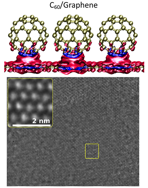
Scientists combined buckyballs, [also known as buckminsterfullerenes, fullerenes, or C60] which resemble tiny soccer balls made from 60 carbon atoms, with graphene, a single layer of carbon, on an underlying surface. Positive and negative charges can transfer between the balls and graphene depending on the nature of the surface as well as the structural order and local orientation of the carbon ball. Scientists can use this architecture to develop tunable junctions for lightweight electronic devices.

The researchers have made this illustration of their work available,

Researchers are developing new, lightweight electronics that rapidly conduct electricity by covering a sheet of carbon (graphene) with buckyballs. Electricity is the flow of electrons. On these lightweight structures, electrons as well as positive holes (missing electrons) transfer between the balls and graphene. The team showed that the crystallinity and orientation of the balls, as well as the underlying layer, affected this charge transfer. The top image shows a calculation of the charge density for a specific orientation of the balls on graphene. The blue represents positive charges, while the red is negative. The bottom image shows that the balls are in a close-packed structure. The bright dots correspond to the projected images of columns of buckyball molecules. Courtesy: US Department of Energy Office of Science

A February 28, 2018 US Department of Energy (DoE) Office of Science news release, which originated the news item, provides more detail,

The Impact

Fast-moving electrons and their counterpart, holes, were preserved in graphene with crystalline buckyball overlayers. Significantly, the carbon ball provides charge transfer to the graphene. Scientists expect the transfer to be highly tunable with external voltages. This marriage has ramifications for smart electronics that run longer and do not break as easily, bringing us closer to sensor-embedded smart clothing and robotic skin.

Summary

Charge transfer at the interface between dissimilar materials is at the heart of almost all electronic technologies such as transistors and photovoltaic devices. In this study, scientists studied charge transfer at the interface region of buckyball molecules deposited on graphene, with and without a supporting substrate, such as hexagonal boron nitride. They employed ab initio density functional theory with van der Waals interactions to model the structure theoretically. Van der Waals interactions are weak connections between neutral molecules. The team used high-resolution transmission electron microscopy and electronic transport measurements to characterize experimentally the properties of the interface. The researchers observed that charge transfer between buckyballs and the graphene was sensitive to the nature of the underlying substrate, in addition, to the crystallinity and local orientation of the buckyballs. These studies open an avenue to devices where buckyball layers on top of graphene can serve as electron acceptors and other buckyball layers as electron donors. Even at room temperature, buckyball molecules were orientationally locked into position. This is in sharp contrast to buckyball molecules in un-doped bulk crystalline configurations, where locking occurs only at low temperature. High electron and hole mobilities are preserved in graphene with crystalline buckyball overlayers. This finding has ramifications for the development of organic high-mobility field-effect devices and other high mobility applications.

Here’s a link to and a citation for the paper,

Molecular Arrangement and Charge Transfer in C60 /Graphene Heterostructures by Claudia Ojeda-Aristizabal, Elton J. G. Santos, Seita Onishi, Aiming Yan, Haider I. Rasool, Salman Kahn, Yinchuan Lv, Drew W. Latzke, Jairo Velasco Jr., Michael F. Crommie, Matthew Sorensen, Kenneth Gotlieb, Chiu-Yun Lin, Kenji Watanabe, Takashi Taniguchi, Alessandra Lanzara, and Alex Zettl. ACS Nano, 2017, 11 (5), pp 4686–4693 DOI: 10.1021/acsnano.7b00551 Publication Date (Web): April 24, 2017

Copyright © 2017 American Chemical Society

This paper is behind a paywall.

Carbon nanotubes one way: gas The other way: flexible sensors*

A Sept. 24, 2013 Technische Universitaet Muenchen (TUM) press release (also on EurekAlert) promises that flexible sensors are on the horizon,

Carbon nanotube-based gas sensors created at TUM offer a unique combination of characteristics that can’t be matched by any of the alternative technologies. They rapidly detect and continuously respond to extremely small changes in the concentrations of gases including ammonia, carbon dioxide, and nitrogen oxide. They operate at room temperature and consume very little power. Furthermore, as the TUM researchers report in their latest papers, such devices can be fabricated on flexible backing materials through large-area, low-cost processes.

Thus it becomes realistic to envision plastic food wrap that incorporates flexible, disposable gas sensors, providing a more meaningful indicator of food freshness than the sell-by date. Measuring carbon dioxide, for example, can help predict the shelf life of meat. “Smart packaging” – assuming consumers find it acceptable and the devices’ non-toxic nature can be demonstrated – could enhance food safety and might also vastly reduce the amount of food that is wasted. Used in a different setting, the same sort of gas sensor could make it less expensive and more practical to monitor indoor air quality in real time.

Dexter Johnson in a Sept. 26, 2013 posting on Nanoclast (an IEEE [Institute of Electrical and Electronics Engineers] blog) warns (Note: Links have been removed),

While this sounds great, the obstacle preventing this from becoming a reality has always been cost. Thin-film sensory packaging may make sense for a high-cost item, but for an inexpensive grocery store product, it’s hard to justify an additional cost that may be as much as the product itself. I made this point nearly a decade ago in report I authored titled, “The Future of Nanotechnology in Printing and Packaging”.

This doesn’t even take into account the often biased opinion people have about nanotechnology in relation to food.

Dexter recommends the researchers focus their commercialization efforts on robotic skins and other high ticket applications.

In reading the description of how the researchers created these flexible sensors, Dexter’s concerns are brought int high relief,

The most basic building block for this technology is a single cylindrical molecule, a rolled-up sheet of carbon atoms that are linked in a honeycomb pattern. This so-called carbon nanotube could be likened to an unimaginably long garden hose: a hollow tube just a nanometer or so in diameter but perhaps millions of times as long as it is wide. Individual carbon nanotubes exhibit amazing and useful properties, but in this case the researchers are more interested in what can be done with them en masse.

Laid down in thin films, randomly oriented carbon nanotubes form conductive networks that can serve as electrodes; patterned and layered films can function as sensors or transistors. “In fact,” Prof. Lugli [Prof. Paolo Lugli, director of TUM’s Nanoelectronics Institute] explains, “the electrical resistivity of such films can be modulated by either an applied voltage (to provide a transistor action) or by the adsorption of gas molecules, which in turn is a signature of the gas concentration for sensor applications.” And as a basis for gas sensors in particular, carbon nanotubes combine advantages (and avoid shortcomings) of more established materials, such as polymer-based organic electronics and solid-state metal-oxide semiconductors. What has been lacking until now is a reliable, reproducible, low-cost fabrication method.

Spray deposition, supplemented if necessary by transfer printing, meets that need. An aqueous solution of carbon nanotubes looks like a bottle of black ink and can be handled in similar ways. Thus devices can be sprayed – from a computer-controlled robotic nozzle – onto virtually any kind of substrate, including large-area sheets of flexible plastic. There is no need for expensive clean-room facilities.

“To us it was important to develop an easily scalable technology platform for manufacturing large-area printed and flexible electronics based on organic semiconductors and nanomaterials,” Abdellah says. “To that end, spray deposition forms the core of our processing technology.”

Remaining technical challenges arise largely from application-specific requirements, such as the need for gas sensors to be selective as well as sensitive.

Here are citations for and links to three of the researchers’ papers,

Fabrication of carbon nanotube thin films on flexible substrates by spray deposition and transfer printing. Ahmed Abdelhalim, Alaa Abdellah, Giuseppe Scarpa, Paolo Lugli. Carbon, Vol. 61, September 2013, 72-79. DOI: 10.1016/j.carbon.2013.04.069

Flexible carbon nanotube-based gas sensors fabricated by large-scale spray deposition.
Alaa Abdellah, Zubair Ahmad, Philipp Köhler, Florin Loghin, Alexander Weise, Giuseppe Scarpa, Paolo Lugli. IEEE Sensors Journal, Vol. 13 Issue 10, October 2013, 4014-4021. DOI: 10.1109/JSEN.2013.2265775

Scalable spray deposition process for high performance carbon nanotube gas sensors. Alaa Abdellah, Ahmed Abdelhalim, Markus Horn, Giuseppe Scarpa, and Paolo Lugli. IEEE Transactions on Nanotechnology 12, 174-181, 2013. DOI: 10.1109/TNANO.2013.2238248

All three papers are behind paywalls.

In one of those coincidences that take place from time to time, I wrote about an upcoming event taking place in the Guardian’s London offices, a panel discussion on nanotechnology and food,in a Sept.  26, 2013 posting.

* In the interest of some clarity the head was changed on March 13, 2015.