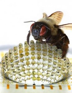
The new digital cameras exploit large arrays of tiny focusing lenses and miniaturized detectors in hemispherical layouts, just like eyes found in arthropods
A May 1, 2013 news item on Nanowerk provides some details about a new ‘bug-eyed’ digital camera,
An interdisciplinary team of researchers has created the first digital cameras with designs that mimic those of ocular systems found in dragonflies, bees, praying mantises and other insects. This class of technology offers exceptionally wide-angle fields of view, with low aberrations, high acuity to motion, and nearly infinite depth of field.
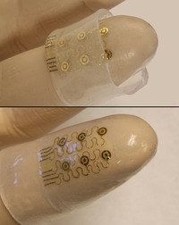
Taking cues from Mother Nature, the cameras exploit large arrays of tiny focusing lenses and miniaturized detectors in hemispherical layouts, just like eyes found in arthropods. The devices combine soft, rubbery optics with high performance silicon electronics and detectors, using ideas first established in research on skin and brain monitoring systems by John A. Rogers, a Swanlund Chair Professor at the University of Illinois at Urbana-Champaign, and his collaborators.
The May 1, 2013 University of Illinois news release by John Kubetz, which originated the news item, describes the special properties of an insect eye and how the camera mimics those properties,
Eyes in arthropods use compound designs, in which arrays of smaller eyes act together to provide image perception. Each small eye, known as an ommatidium, consists of a corneal lens, a crystalline cone, and a light sensitive organ at the base. The entire system is configured to provide exceptional properties in imaging, many of which lie beyond the reach of existing man-made cameras.
The researchers developed new ideas in materials and fabrication strategies allowing construction of artificial ommatidia in large, interconnected arrays in hemispherical layouts. Building such systems represents a daunting task, as all established camera technologies rely on bulk glass lenses and detectors constructed on the planar surfaces of silicon wafers which cannot be bent or flexed, much less formed into a hemispherical shape.
“A critical feature of our fly’s eye cameras is that they incorporate integrated microlenses, photodetectors, and electronics on hemispherically curved surfaces,” said Jianliang Xiao, an assistant professor of mechanical engineering at University of Colorado Boulder and coauthor of the study. “To realize this outcome, we used soft, rubbery optics bonded to detectors/electronics in mesh layouts that can be stretched and deformed, reversibly and without damage.”
On a more technical note, from the news release,
The fabrication starts with electronics, detectors and lens arrays formed on flat surfaces using advanced techniques adapted from the semiconductor industry, said Xiao [Jianliang Xiao, an assistant professor of mechanical engineering at University of Colorado Boulder and coauthor of the study], who began working on the project as a postdoctoral researcher in Rogers’ lab at Illinois. The lens sheet—made from a polymer material similar to a contact lens—and the electronics/detectors are then aligned and bonded together. Pneumatic pressure deforms the resulting system into the desired hemispherical shape, in a process much like blowing up a balloon, but with precision engineering control.
The individual electronic detectors and microlenses are coupled together to avoid any relative motion during this deformation process. Here, the spaces between these artificial ommatidia can stretch to allow transformation in geometry from planar to hemispherical. The electrical interconnections are thin, and narrow, in filamentary serpentine shapes; they deform as tiny springs during the stretching process.
According to the researchers, each microlens produces a small image of an object with a form dictated by the parameters of the lens and the viewing angle. An individual detector responds only if a portion of the image formed by the associated microlens overlaps the active area. The detectors stimulated in this way produce a sampled image of the object that can then be reconstructed using models of the optics.
Katherine Bourzac in her May 1, 2013 article for Nature magazine provides some additional insight and a perspective (intentional wordplay) from a researcher who has an idea of how he might like to integrate this new type of camera into his own work,
Insect eyes are made up of hundreds or even thousands of light-sensing structures called ommatidia. Each contains a lens and a cone that funnels light to a photosensitive organ. The long, thin ommatidia are bunched together to form the hemispherical eye, with each ommatidium pointing in a slightly different direction. This structure gives bugs a wide field of view, with objects in the periphery just as clear as those in the centre of the visual field, and high motion sensitivity. It also allows a large depth of field — objects are in focus whether they’re nearby or at a distance.
…
“The whole thing [the new digital camera] is stretchy and thin, and we blow it up like a balloon” so that it curves like a compound eye, says Rogers. The current prototype produces black-and-white images only, but Rogers says a colour version could be made with the same design.
…
With the basic designs in place, Rogers says, his team can now increase the resolution of the camera by incorporating more ommatidia. “We’d like to do a dragonfly, with 20,000 ommatidia,” he says, which will require some miniaturization of the components.
Alexander Borst, who builds miniature flying robots at the Max Planck Institute of Neurobiology in Martinsried, Germany, says that he is eager to integrate the camera into his machines. Insects’ wide field of vision helps them to monitor and stabilize their position during flight; robots with artificial compound eyes might be better fliers, he says.
For interested parties, here’s a link to and a citation for the research paper,
Digital cameras with designs inspired by the arthropod eye by Young Min Song, Yizhu Xie, Viktor Malyarchuk, Jianliang Xiao, Inhwa Jung, Ki-Joong Choi, Zhuangjian Liu, Hyunsung Park, Chaofeng Lu, Rak-Hwan Kim, Rui Li, Kenneth B. Crozier, Yonggang Huang, & John A. Rogers.
Nature 497, 95–99 (02 May 2013) doi:10.1038/nature12083 Published online 01 May 2013
This article is behind a paywall.
I last mentioned John A. Rogers and the University of Illinois in a Feb. 28, 2013 posting about a bendable, stretchable lithium-ion battery.
