Here’s a look at the cars:
A March 11, 2022 news item on Nanowerk announces the upcoming 2nd NanoCar race,
The world’s smallest car race will return to Toulouse (southwestern France) on 24-25 March. Eight international teams will be at the starting line for the competition. Christian Joachim, a CNRS [Centre national de la recherche scientifique] research professor and the event organiser, provides details regarding the issues involved.
Event: NanoCar Race II, March 24-25, 2022 at CEMES [Centre d’Élaboration de Matériaux et d’Etudes Structurales] (La Boule), in Toulouse. The race will be broadcast on the event’s YouTube channel: https://www.youtube.com/channel/UCkQixqt0xegeVEmo9y9gMXQ
…
A March 7, 2022 CNRS press release written by Grégory Fléchet, which originated the news item, proceeds in an interview format accompanied by footnotes, Note 1: Links have been removed; Note 2: The press release is illustrated with numerous embedded images,
Five years after the first NanoCar Race, this new and – to say the least – unique race is finally returning to the CEMES.1 Why such a long wait?
Christian Joachim:2 The very first molecule-car race in April 2017 required four years of preparation. For this second edition, the call for applications was made in March 2018, with a view to holding the competition in Toulouse in 2020. In late 2019, the international organising committee selected 11 teams from the 23 statements of intent submitted from all continents. Everything was in place for the race to be held in the spring of 2020. Unfortunately the Covid-19 epidemic broke out, forcing us to put the event on standby until July 2021. After this long break, only eight teams remained. We interviewed them by videoconference in September 2021, with support from the French embassies in their respective countries as well as the CNRS offices abroad, in order to confirm their level of commitment. The eight teams then travelled to Toulouse on 23 November, 2021 to officially present their molecule-car during C’NANO 2021. Together we set a date for the race.
…
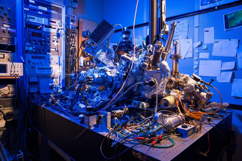
How does the scanning tunneling microscope that will capture the images of the race and fuel the molecule-cars operate?
C. J.: We are mostly using the imaging function of the scanning tunneling microscope (STM). With a single atom at its tip, this high-precision instrument can scan a material’s surface, while keeping that surface less than a nanometre away from the particle. At that distance, a “tunneling” current is established, on the order of 1 nanoampere for 1 volt of applied voltage. This weak current converted into an amplified voltage can stabilise the distance between the tip and the surface without them touching. This enables us to produce, line by line, an image of the observed material.
For greater precision, the scanning should be performed at a temperature near absolute zero, around -270 °C. This prevents the atoms that make up the track’s surface from being tossed about by thermal agitation. Once the molecule-car is on the racetrack, the driver uses the tip of the STM to supply energy and move the vehicle forward. To do this, the pilot can increase the voltage between the tip and the surface, or can leave the former at the same place on the molecule-car for a certain amount of time, between 100 milliseconds and a few seconds. In this latter scenario, the tunnel current’s small inelastic effect through the molecule-car increases the vibrational energy of some of its mechanical degrees of freedom, which moves the car forward step by step, generally a few hundred picometres at a time (1 pm=10-12m).
Can you describe the structure of the track on which the nanocars will race?
C. J.: The track was created on the surface of a pure gold crystal – in this case a pastille 8 mm in diameter – naturally featuring small grooves. These folds, which minimise the gold crystal’s surface energy, are arranged in straight lines of 100 to 200 nm, forming lanes for the molecule-cars. Track length differs from one gold pastille to another, as does the arrangement of narrow and wide grooves, which generally vary between 4-10 nm.
This layout depends on the preparation methods used by each competitor. At the end of each straight line in a given track, groups of atoms on the surface shift slightly, thereby creating a small bend – measuring between 4-5 nm with a curve of 20-30° – that connects it with the next straight line. This is the chief difficulty of the race, as a molecule-car can easily end up stuck on a bend. During the first NanoCar Race, drivers noticed that the most effective way to negotiate a turn was to bypass it on the right or left by following the next track.
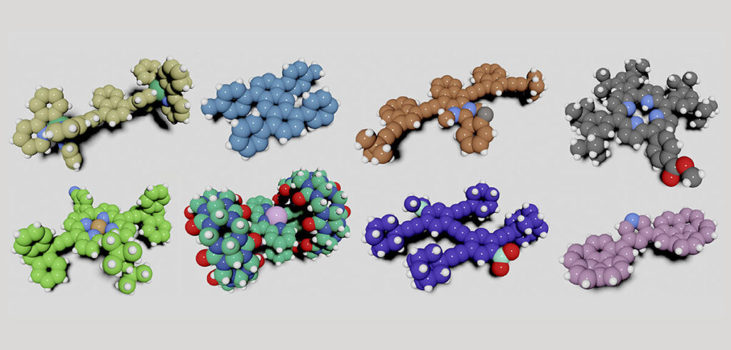
This year eight teams will compete.4 What do their nanocars look like?
C. J.: Some molecule-cars, like the one from the Strasbourg Institute of Chemistry, have two wheels and a central chassis. Others, including that developed by the Spanish team from the Nanoscience IMDEA, have four wheels attached to a chassis. Those of the Japanese and French-Japanese teams have two wheels with paddles, and a foot at the back to protect the chassis from being crushed against the track’s surface. A dipole moment can be included in the frame via a small chemical grouping located at the front of the molecule. The prototype from Ohio University has two enormous wheels attached to a narrow chassis. The latter remains an essential feature regardless of the vehicle’s chemical structure. By raising the molecular structure to which the wheels or paddles are attached, the chassis reduces the molecule-car’s interactions with the track’s surface.
…
I can’t find a specific start time but the 2nd NanoCar Race will be livestreamed for 24 hours March 24 – 25, 2022 on the event’s YouTube channel: https://www.youtube.com/channel/UCkQixqt0xegeVEmo9y9gMXQ.
For the curious, I recommend reading the March 7, 2022 CNRS press release in its entirety.
Finally, this is my fourth posting about this race. For the diehards:
- July 9, 2020 Getting ready for the next nano Grand Prix in 2021
- December 18, 2020 Next-gen Rice University nanocars for Second international Nanocar Race (it’s been bumped to 2022)
- December 28, 2021 2nd international Nanocar Race to be broadcast live in March 2022
Enjoy race day!