Tag Archives: sensors

Artificial intelligence and industrial applications

This is take on artificial intelligence that I haven’t encountered before. Sean Captain’s Nov. 15, 2016 article for Fast Company profiles industry giant GE (General Electric) and its foray into that world (Note: Links have been removed),

When you hear the term “artificial intelligence,” you may think of tech giants Amazon, Google, IBM, Microsoft, or Facebook. Industrial powerhouse General Electric is now aiming to be included on that short list. It may not have a chipper digital assistant like Cortana or Alexa. It won’t sort through selfies, but it will look through X-rays. It won’t recommend movies, but it will suggest how to care for a diesel locomotive. Today, GE announced a pair of acquisitions and new services that will bring machine learning AI to the kinds of products it’s known for, including planes, trains, X-ray machines, and power plants.

The effort started in 2015 when GE announced Predix Cloud—an online platform to network and collect data from sensors on industrial machinery such as gas turbines or windmills. At the time, GE touted the benefits of using machine learning to find patterns in sensor data that could lead to energy savings or preventative maintenance before a breakdown. Predix Cloud opened up to customers in February [2016?], but GE is still building up the AI capabilities to fulfill the promise. “We were using machine learning, but I would call it in a custom way,” says Bill Ruh, GE’s chief digital officer and CEO of its GE Digital business (GE calls its division heads CEOs). “And we hadn’t gotten to a general-purpose framework in machine learning.”

Today [Nov. 15, 2016] GE revealed the purchase of two AI companies that Ruh says will get them there. Bit Stew Systems, founded in 2005, was already doing much of what Predix Cloud promises—collecting and analyzing sensor data from power utilities, oil and gas companies, aviation, and factories. (GE Ventures has funded the company.) Customers include BC Hydro, Pacific Gas & Electric, and Scottish & Southern Energy.

The second purchase, Wise.io is a less obvious purchase. Founded by astrophysics and AI experts using machine learning to study the heavens, the company reapplied the tech to streamlining a company’s customer support systems, picking up clients like Pinterest, Twilio, and TaskRabbit. GE believes the technology will transfer yet again, to managing industrial machines. “I think by the middle of next year we will have a full machine learning stack,” says Ruh.

Though young, Predix is growing fast, with 270 partner companies using the platform, according to GE, which expects revenue on software and services to grow over 25% this year, to more than $7 billion. Ruh calls Predix a “significant part” of that extra money. And he’s ready to brag, taking a jab at IBM Watson for being a “general-purpose” machine-learning provider without the deep knowledge of the industries it serves. “We have domain algorithms, on machine learning, that’ll know what a power plant is and all the depth of that, that a general-purpose machine learning will never really understand,” he says.

One especially dull-sounding new Predix service—Predictive Corrosion Management—touches on a very hot political issue: giant oil and gas pipeline projects. Over 400 people have been arrested in months of protests against the Dakota Access Pipeline, which would carry crude oil from North Dakota to Illinois. The issue is very complicated, but one concern of protestors is that a pipeline rupture would contaminate drinking water for the Standing Rock Sioux reservation.

“I think absolutely this is aimed at that problem. If you look at why pipelines spill, it’s corrosion,” says Ruh. “We believe that 10 years from now, we can detect a leak before it occurs and fix it before you see it happen.” Given how political battles over pipelines drag on, 10 years might not be so long to wait.

I recommend reading the article in its entirety if you have the time. And, for those of us in British Columbia, Canada, it was a surprise to see BC Hydro on the list of customers for one of GE’s new acquisitions. As well, that business about the pipelines hits home hard given the current debates (Enbridge Northern Gateway Pipelines) here. *ETA Dec. 27, 2016: This was originally edited just prior to publication to include information about the announcement by the Trudeau cabinet approving two pipelines for TransMountain  and Enbridge respectively while rejecting the Northern Gateway pipeline (Canadian Broadcasting Corporation [CBC] online news Nov. 29, 2016).  I trust this second edit will stick.*

It seems GE is splashing out in a big way. There’s a second piece on Fast Company, a Nov. 16, 2016 article by Sean Captain (again) this time featuring a chat between an engineer and a robotic power plant,

We are entering the era of talking machines—and it’s about more than just asking Amazon’s Alexa to turn down the music. General Electric has built a digital assistant into its cloud service for managing power plants, jet engines, locomotives, and the other heavy equipment it builds. Over the internet, an engineer can ask a machine—even one hundreds of miles away—how it’s doing and what it needs. …

Voice controls are built on top of GE’s Digital Twin program, which uses sensor readings from machinery to create virtual models in cyberspace. “That model is constantly getting a stream of data, both operational and environmental,” says Colin Parris, VP at GE Software Research. “So it’s adapting itself to that type of data.” The machines live virtual lives online, allowing engineers to see how efficiently each is running and if they are wearing down.

GE partnered with Microsoft on the interface, using the Bing Speech API (the same tech powering the Cortana digital assistant), with special training on key terms like “rotor.” The twin had little trouble understanding the Mandarin Chinese accent of Bo Yu, one of the researchers who built the system; nor did it stumble on Parris’s Trinidad accent. Digital Twin will also work with Microsoft’s HoloLens mixed reality goggles, allowing someone to step into a 3D image of the equipment.

I can’t help wondering if there are some jobs that were eliminated with this technology.

Spinach and plant nanobionics

Who knew that spinach leaves could be turned into electronic devices? The answer is: engineers at the Massachusetts Institute of Technology, according to an Oct. 31, 2016 news item on phys.org,

Spinach is no longer just a superfood: By embedding leaves with carbon nanotubes, MIT engineers have transformed spinach plants into sensors that can detect explosives and wirelessly relay that information to a handheld device similar to a smartphone.

This is one of the first demonstrations of engineering electronic systems into plants, an approach that the researchers call “plant nanobionics.”

An Oct. 31, 2016 MIT news release (also on EurekAlert), which originated the news item, describes the research further (Note: Links have been removed),

“The goal of plant nanobionics is to introduce nanoparticles into the plant to give it non-native functions,” says Michael Strano, the Carbon P. Dubbs Professor of Chemical Engineering at MIT and the leader of the research team.

In this case, the plants were designed to detect chemical compounds known as nitroaromatics, which are often used in landmines and other explosives. When one of these chemicals is present in the groundwater sampled naturally by the plant, carbon nanotubes embedded in the plant leaves emit a fluorescent signal that can be read with an infrared camera. The camera can be attached to a small computer similar to a smartphone, which then sends an email to the user.

“This is a novel demonstration of how we have overcome the plant/human communication barrier,” says Strano, who believes plant power could also be harnessed to warn of pollutants and environmental conditions such as drought.

Strano is the senior author of a paper describing the nanobionic plants in the Oct. 31 [2016] issue of Nature Materials. The paper’s lead authors are Min Hao Wong, an MIT graduate student who has started a company called Plantea to further develop this technology, and Juan Pablo Giraldo, a former MIT postdoc who is now an assistant professor at the University of California at Riverside.

Environmental monitoring

Two years ago, in the first demonstration of plant nanobionics, Strano and former MIT postdoc Juan Pablo Giraldo used nanoparticles to enhance plants’ photosynthesis ability and to turn them into sensors for nitric oxide, a pollutant produced by combustion.

Plants are ideally suited for monitoring the environment because they already take in a lot of information from their surroundings, Strano says.

“Plants are very good analytical chemists,” he says. “They have an extensive root network in the soil, are constantly sampling groundwater, and have a way to self-power the transport of that water up into the leaves.”

Strano’s lab has previously developed carbon nanotubes that can be used as sensors to detect a wide range of molecules, including hydrogen peroxide, the explosive TNT, and the nerve gas sarin. When the target molecule binds to a polymer wrapped around the nanotube, it alters the tube’s fluorescence.

In the new study, the researchers embedded sensors for nitroaromatic compounds into the leaves of spinach plants. Using a technique called vascular infusion, which involves applying a solution of nanoparticles to the underside of the leaf, they placed the sensors into a leaf layer known as the mesophyll, which is where most photosynthesis takes place.

They also embedded carbon nanotubes that emit a constant fluorescent signal that serves as a reference. This allows the researchers to compare the two fluorescent signals, making it easier to determine if the explosive sensor has detected anything. If there are any explosive molecules in the groundwater, it takes about 10 minutes for the plant to draw them up into the leaves, where they encounter the detector.

To read the signal, the researchers shine a laser onto the leaf, prompting the nanotubes in the leaf to emit near-infrared fluorescent light. This can be detected with a small infrared camera connected to a Raspberry Pi, a $35 credit-card-sized computer similar to the computer inside a smartphone. The signal could also be detected with a smartphone by removing the infrared filter that most camera phones have, the researchers say.

“This setup could be replaced by a cell phone and the right kind of camera,” Strano says. “It’s just the infrared filter that would stop you from using your cell phone.”

Using this setup, the researchers can pick up a signal from about 1 meter away from the plant, and they are now working on increasing that distance.

Michael McAlpine, an associate professor of mechanical engineering at the University of Minnesota, says this approach holds great potential for engineering not only sensors but many other kinds of bionic plants that might receive radio signals or change color.

“When you have manmade materials infiltrated into a living organism, you can have plants do things that plants don’t ordinarily do,” says McAlpine, who was not involved in the research. “Once you start to think of living organisms like plants as biomaterials that can be combined with electronic materials, this is all possible.”

“A wealth of information”

In the 2014 plant nanobionics study, Strano’s lab worked with a common laboratory plant known as Arabidopsis thaliana. However, the researchers wanted to use common spinach plants for the latest study, to demonstrate the versatility of this technique. “You can apply these techniques with any living plant,” Strano says.

So far, the researchers have also engineered spinach plants that can detect dopamine, which influences plant root growth, and they are now working on additional sensors, including some that track the chemicals plants use to convey information within their own tissues.

“Plants are very environmentally responsive,” Strano says. “They know that there is going to be a drought long before we do. They can detect small changes in the properties of soil and water potential. If we tap into those chemical signaling pathways, there is a wealth of information to access.”

These sensors could also help botanists learn more about the inner workings of plants, monitor plant health, and maximize the yield of rare compounds synthesized by plants such as the Madagascar periwinkle, which produces drugs used to treat cancer.

“These sensors give real-time information from the plant. It is almost like having the plant talk to us about the environment they are in,” Wong says. “In the case of precision agriculture, having such information can directly affect yield and margins.”

Once getting over the excitement, questions spring to mind. How could this be implemented? Is somebody  going to plant a field of spinach and then embed the leaves so they can detect landmines? How will anyone know where to plant the spinach? And on a different track, is this spinach edible? I suspect that if spinach can be successfully used as a sensor, it might not be for explosives but for pollution as the researchers suggest.

Here’s a link to and a citation for the paper,

Nitroaromatic detection and infrared communication from wild-type plants using plant nanobionics by Min Hao Wong, Juan P. Giraldo, Seon-Yeong Kwak, Volodymyr B. Koman, Rosalie Sinclair, Tedrick Thomas Salim Lew, Gili Bisker, Pingwei Liu, & Michael S. Strano. Nature Materials (2016) doi:10.1038/nmat4771 Published online 31 October 2016

This paper is behind a paywall.

The last posting here which featured Strano’s research is in an Aug. 25, 2015 piece about carbon nanotubes and medical sensors.

Atomic force microscope with nanowire sensors

Measuring the size and direction of forces may become reality with a nanotechnology-enabled atomic force microscope designed by Swiss scientists, according to an Oct. 17, 2016 news item on phys.org,

A new type of atomic force microscope (AFM) uses nanowires as tiny sensors. Unlike standard AFM, the device with a nanowire sensor enables measurements of both the size and direction of forces. Physicists at the University of Basel and at the EPF Lausanne have described these results in the recent issue of Nature Nanotechnology.

A nanowire sensor measures size and direction of forces (Image: University of Basel, Department of Physics)

A nanowire sensor measures size and direction of forces (Image: University of Basel, Department of Physics)

An Oct. 17, 2016 University of Basel press release (also on EurekAlert), which originated the news item, expands on the theme,

Nanowires are extremely tiny filamentary crystals which are built-up molecule by molecule from various materials and which are now being very actively studied by scientists all around the world because of their exceptional properties.

The wires normally have a diameter of 100 nanometers and therefore possess only about one thousandth of a hair thickness. Because of this tiny dimension, they have a very large surface in comparison to their volume. This fact, their small mass and flawless crystal lattice make them very attractive in a variety of nanometer-scale sensing applications, including as sensors of biological and chemical samples, and as pressure or charge sensors.

Measurement of direction and size

The team of Argovia Professor Martino Poggio from the Swiss Nanoscience Institute (SNI) and the Department of Physics at the University of Basel has now demonstrated that nanowires can also be used as force sensors in atomic force microscopes. Based on their special mechanical properties, nanowires vibrate along two perpendicular axes at nearly the same frequency. When they are integrated into an AFM, the researchers can measure changes in the perpendicular vibrations caused by different forces. Essentially, they use the nanowires like tiny mechanical compasses that point out both the direction and size of the surrounding forces.

Image of the two-dimensional force field

The scientists from Basel describe how they imaged a patterned sample surface using a nanowire sensor. Together with colleagues from the EPF Lausanne, who grew the nanowires, they mapped the two-dimensional force field above the sample surface using their nanowire “compass”. As a proof-of-principle, they also mapped out test force fields produced by tiny electrodes.

The most challenging technical aspect of the experiments was the realization of an apparatus that could simultaneously scan a nanowire above a surface and monitor its vibration along two perpendicular directions. With their study, the scientists have demonstrated a new type of AFM that could extend the technique’s numerous applications even further.

AFM – today widely used

The development of AFM 30 years ago was honored with the conferment of the Kavli-Prize [2016 Kavli Prize in Nanoscience] beginning of September this year. Professor Christoph Gerber of the SNI and Department of Physics at the University of Basel is one of the awardees, who has substantially contributed to the wide use of AFM in different fields, including solid-state physics, materials science, biology, and medicine.

The various different types of AFM are most often carried out using cantilevers made from crystalline Si as the mechanical sensor. “Moving to much smaller nanowire sensors may now allow for even further improvements on an already amazingly successful technique”, Martino Poggio comments his approach.

I featured an interview article with Christoph Gerber and Gerd Binnig about their shared Kavli prize and about inventing the AFM in a Sept. 20, 2016 posting.

As for the latest innovation, here’s a link to and a citation for the paper,

Vectorial scanning force microscopy using a nanowire sensor by Nicola Rossi, Floris R. Braakman, Davide Cadeddu, Denis Vasyukov, Gözde Tütüncüoglu, Anna Fontcuberta i Morral, & Martino Poggio. Nature Nanotechnology (2016) doi:10.1038/nnano.2016.189 Published online 17 October 2016

This paper is behind a paywall.

Tiny sensors produced by nanoscale 3D printing could lead to new generation of atomic force microscopes

A Sept. 26, 2016 news item on Nanowerk features research into producing smaller sensors for atomic force microscopes (AFMs) to achieve greater sensitivity,

Tiny sensors made through nanoscale 3D printing may be the basis for the next generation of atomic force microscopes. These nanosensors can enhance the microscopes’ sensitivity and detection speed by miniaturizing their detection component up to 100 times. The sensors were used in a real-world application for the first time at EPFL, and the results are published in Nature Communications.

A Sept. 26, 2016 École Polytechnique Fédérale de Lausanne (EPFL; Switzerland) press release by Laure-Anne Pessina, which originated the news item, expands on the theme (Note: A link has been removed),

Atomic force microscopy is based on powerful technology that works a little like a miniature turntable. A tiny cantilever with a nanometric tip passes over a sample and traces its relief, atom by atom. The tip’s infinitesimal up-and-down movements are picked up by a sensor so that the sample’s topography can be determined. (…)

One way to improve atomic force microscopes is to miniaturize the cantilever, as this will reduce inertia, increase sensitivity, and speed up detection. Researchers at EPFL’s Laboratory for Bio- and Nano-Instrumentation achieved this by equipping the cantilever with a 5-nanometer thick sensor made with a nanoscale 3D-printing technique. “Using our method, the cantilever can be 100 times smaller,” says Georg Fantner, the lab’s director.

Electrons that jump over obstacles

The nanometric tip’s up-and-down movements can be measured through the deformation of the sensor placed at the fixed end of the cantilever. But because the researchers were dealing with minute movements – smaller than an atom – they had to pull a trick out of their hat.

Together with Michael Huth’s lab at Goethe Universität at Frankfurt am Main, they developed a sensor made up of highly conductive platinum nanoparticles surrounded by an insulating carbon matrix. Under normal conditions, the carbon isolates the electrons. But at the nano-scale, a quantum effect comes into play: some electrons jump through the insulating material and travel from one nanoparticle to the next. “It’s sort of like if people walking on a path came up against a wall and only the courageous few managed to climb over it,” said Fantner.

When the shape of the sensor changes, the nanoparticles move further away from each other and the electrons jump between them less frequently. Changes in the current thus reveal the deformation of the sensor and the composition of the sample.

Tailor-made sensors

The researchers’ real feat was in finding a way to produce these sensors in nanoscale dimensions while carefully controlling their structure and, by extension, their properties. “In a vacuum, we distribute a precursor gas containing platinum and carbon atoms over a substrate. Then we apply an electron beam. The platinum atoms gather and form nanoparticles, and the carbon atoms naturally form a matrix around them,” said Maja Dukic, the article’s lead author. “By repeating this process, we can build sensors with any thickness and shape we want. We have proven that we could build these sensors and that they work on existing infrastructures. Our technique can now be used for broader applications, ranging from biosensors, ABS sensors for cars, to touch sensors on flexible membranes in prosthetics and artificial skin.”

Here’s a link to and a citation for the paper,

Direct-write nanoscale printing of nanogranular tunnelling strain sensors for sub-micrometre cantilevers by Maja Dukic, Marcel Winhold, Christian H. Schwalb, Jonathan D. Adams, Vladimir Stavrov, Michael Huth, & Georg E. Fantner. Nature Communications 7, Article number: 12487 doi:10.1038/ncomms12487 Published  26 September 2016

This is an open access paper.

Sutures that can gather data wirelessly

Are sutures which gather data hackable? It’s a little early to start thinking about that issue as this seems to be brand new research. A July 18, 2016 news item on ScienceDaily tells more,

For the first time, researchers led by Tufts University engineers have integrated nano-scale sensors, electronics and microfluidics into threads — ranging from simple cotton to sophisticated synthetics — that can be sutured through multiple layers of tissue to gather diagnostic data wirelessly in real time, according to a paper published online July 18 [2016] in Microsystems & Nanoengineering. The research suggests that the thread-based diagnostic platform could be an effective substrate for a new generation of implantable diagnostic devices and smart wearable systems.

A July 18, 2016 Tufts University news release (also on EurekAlert), which originated the news item, provides more detail,

The researchers used a variety of conductive threads that were dipped in physical and chemical sensing compounds and connected to wireless electronic circuitry to create a flexible platform that they sutured into tissue in rats as well as in vitro. The threads collected data on tissue health (e.g. pressure, stress, strain and temperature), pH and glucose levels that can be used to determine such things as how a wound is healing, whether infection is emerging, or whether the body’s chemistry is out of balance. The results were transmitted wirelessly to a cell phone and computer.

The three-dimensional platform is able to conform to complex structures such as organs, wounds or orthopedic implants.

While more study is needed in a number of areas, including investigation of long-term biocompatibility, researchers said initial results raise the possibility of optimizing patient-specific treatments.

“The ability to suture a thread-based diagnostic device intimately in a tissue or organ environment in three dimensions adds a unique feature that is not available with other flexible diagnostic platforms,” said Sameer Sonkusale, Ph.D., corresponding author on the paper and director of the interdisciplinary Nano Lab in the Department of Electrical and Computer Engineering at Tufts School of Engineering. “We think thread-based devices could potentially be used as smart sutures for surgical implants, smart bandages to monitor wound healing, or integrated with textile or fabric as personalized health monitors and point-of-care diagnostics.”

Until now, the structure of substrates for implantable devices has essentially been two-dimensional, limiting their usefulness to flat tissue such as skin, according to the paper. Additionally, the materials in those substrates are expensive and require specialized processing.

Here’s a link to and a citation for the paper,

A toolkit of thread-based microfluidics, sensors, and electronics for 3D tissue embedding for medical diagnostics by Pooria Mostafalu, Mohsen Akbari, Kyle A. Alberti, Qiaobing Xu, Ali Khademhosseini, & Sameer R. Sonkusale. Microsystems & Nanoengineering 2, Article number: 16039 (2016) doi:10.1038/micronano.2016.39 Published online 18 July 2016

This paper is open access.

Wireless, wearable carbon nanotube-based gas sensors for soldiers

Researchers at MIT (Massachusetts Institute of Technology) are hoping to make wireless, toxic gas detectors the size of badges. From a June 30, 2016 news item on Nanowerk,

MIT researchers have developed low-cost chemical sensors, made from chemically altered carbon nanotubes, that enable smartphones or other wireless devices to detect trace amounts of toxic gases.

Using the sensors, the researchers hope to design lightweight, inexpensive radio-frequency identification (RFID) badges to be used for personal safety and security. Such badges could be worn by soldiers on the battlefield to rapidly detect the presence of chemical weapons — such as nerve gas or choking agents — and by people who work around hazardous chemicals prone to leakage.

A June 30, 2016 MIT news release (also on EurekAlert), which originated the news item, describes the technology further,

“Soldiers have all this extra equipment that ends up weighing way too much and they can’t sustain it,” says Timothy Swager, the John D. MacArthur Professor of Chemistry and lead author on a paper describing the sensors that was published in the Journal of the American Chemical Society. “We have something that would weigh less than a credit card. And [soldiers] already have wireless technologies with them, so it’s something that can be readily integrated into a soldier’s uniform that can give them a protective capacity.”

The sensor is a circuit loaded with carbon nanotubes, which are normally highly conductive but have been wrapped in an insulating material that keeps them in a highly resistive state. When exposed to certain toxic gases, the insulating material breaks apart, and the nanotubes become significantly more conductive. This sends a signal that’s readable by a smartphone with near-field communication (NFC) technology, which allows devices to transmit data over short distances.

The sensors are sensitive enough to detect less than 10 parts per million of target toxic gases in about five seconds. “We are matching what you could do with benchtop laboratory equipment, such as gas chromatographs and spectrometers, that is far more expensive and requires skilled operators to use,” Swager says.

Moreover, the sensors each cost about a nickel to make; roughly 4 million can be made from about 1 gram of the carbon nanotube materials. “You really can’t make anything cheaper,” Swager says. “That’s a way of getting distributed sensing into many people’s hands.”

The paper’s other co-authors are from Swager’s lab: Shinsuke Ishihara, a postdoc who is also a member of the International Center for Materials Nanoarchitectonics at the National Institute for Materials Science, in Japan; and PhD students Joseph Azzarelli and Markrete Krikorian.

Wrapping nanotubes

In recent years, Swager’s lab has developed other inexpensive, wireless sensors, called chemiresistors, that have detected spoiled meat and the ripeness of fruit, among other things [go to the end of this post for links to previous posts about Swager’s work]. All are designed similarly, with carbon nanotubes that are chemically modified, so their ability to carry an electric current changes when exposed to a target chemical.

This time, the researchers designed sensors highly sensitive to “electrophilic,” or electron-loving, chemical substances, which are often toxic and used for chemical weapons.

To do so, they created a new type of metallo-supramolecular polymer, a material made of metals binding to polymer chains. The polymer acts as an insulation, wrapping around each of the sensor’s tens of thousands of single-walled carbon nanotubes, separating them and keeping them highly resistant to electricity. But electrophilic substances trigger the polymer to disassemble, allowing the carbon nanotubes to once again come together, which leads to an increase in conductivity.

In their study, the researchers drop-cast the nanotube/polymer material onto gold electrodes, and exposed the electrodes to diethyl chlorophosphate, a skin irritant and reactive simulant of nerve gas. Using a device that measures electric current, they observed a 2,000 percent increase in electrical conductivity after five seconds of exposure. Similar conductivity increases were observed for trace amounts of numerous other electrophilic substances, such as thionyl chloride (SOCl2), a reactive simulant in choking agents. Conductivity was significantly lower in response to common volatile organic compounds, and exposure to most nontarget chemicals actually increased resistivity.

Creating the polymer was a delicate balancing act but critical to the design, Swager says. As a polymer, the material needs to hold the carbon nanotubes apart. But as it disassembles, its individual monomers need to interact more weakly, letting the nanotubes regroup. “We hit this sweet spot where it only works when it’s all hooked together,” Swager says.

Resistance is readable

To build their wireless system, the researchers created an NFC tag that turns on when its electrical resistance dips below a certain threshold.

Smartphones send out short pulses of electromagnetic fields that resonate with an NFC tag at radio frequency, inducing an electric current, which relays information to the phone. But smartphones can’t resonate with tags that have a resistance higher than 1 ohm.

The researchers applied their nanotube/polymer material to the NFC tag’s antenna. When exposed to 10 parts per million of SOCl2 for five seconds, the material’s resistance dropped to the point that the smartphone could ping the tag. Basically, it’s an “on/off indicator” to determine if toxic gas is present, Swager says.

According to the researchers, such a wireless system could be used to detect leaks in Li-SOCl2 (lithium thionyl chloride) batteries, which are used in medical instruments, fire alarms, and military systems.

The next step, Swager says, is to test the sensors on live chemical agents, outside of the lab, which are more dispersed and harder to detect, especially at trace levels. In the future, there’s also hope for developing a mobile app that could make more sophisticated measurements of the signal strength of an NFC tag: Differences in the signal will mean higher or lower concentrations of a toxic gas. “But creating new cell phone apps is a little beyond us right now,” Swager says. “We’re chemists.”

Here’s a link to and a citation for the paper,

Ultratrace Detection of Toxic Chemicals: Triggered Disassembly of Supramolecular Nanotube Wrappers by Shinsuke Ishihara, Joseph M. Azzarelli, Markrete Krikorian, and Timothy M. Swager. J. Am. Chem. Soc., Article ASAP DOI: 10.1021/jacs.6b03869 Publication Date (Web): June 23, 2016

Copyright © 2016 American Chemical Society

This paper is behind a paywall.

Here are links to other posts about Swager’s work featured here previously:

Carbon nanotubes sense spoiled food (April 23, 2015 post)

Smart suits for US soldiers—an update of sorts from the Lawrence Livermore National Laboratory (Feb. 25, 2014 post)

Come, see my etchings … they detect poison gases (Oct. 9, 2012 post)

Soldiers sniff overripe fruit (May 1, 2012 post)

King Abdullah University of Science and Technology (Saudi Arabia) develops sensors from household materials

Researchers at the King Adbullah University of Science and Technology (KAUST) are developing sensors made of household materials according to a Feb. 19, 2016 KAUST news release (also on EurekAlert but dated Feb. 21, 2016),

Everyday materials from the kitchen drawer, such as aluminum foil, sticky note paper, sponges and tape, have been used by a team of electrical engineers from KAUST to develop a low-cost sensor that can detect external stimuli, including touch, pressure, temperature, acidity and humidity.

The sensor, which is called Paper Skin, performs as well as other artificial skin applications currently being developed while integrating multiple functions using cost-effective materials1.

“This work has the potential to revolutionize the electronics industry and opens the door to commercializing affordable high-performance sensing devices,” stated Muhammad Mustafa Hussain from the University’s Integrated Nanotechnology Lab, where the research was conducted.

Wearable and flexible electronics show promise for a variety of applications, such as wireless monitoring of patient health and touch-free computer interfaces. Current research in this direction employs expensive and sophisticated materials and processes.

The team used sticky note paper to detect humidity, sponges and wipes to detect pressure and aluminum foil to detect motion. Coloring a sticky note with an HB pencil allowed the paper to detect acidity levels, and aluminum foil and conductive silver ink were used to detect temperature differences.

The materials were put together into a simple paper-based platform that was then connected to a device that detected changes in electrical conductivity according to external stimuli.

Increasing levels of humidity, for example, increased the platform’s ability to store an electrical charge, or its capacitance. Exposing the sensor to an acidic solution increased its resistance, while exposing it to an alkaline solution decreased it. Voltage changes were detected with temperature changes. Bringing a finger closer to the platform disturbed its electromagnetic field, decreasing its capacitance.

The team leveraged the various properties of the materials they used, including their porosity, adsorption, elasticity and dimensions to develop the low-cost sensory platform. They also demonstrated that a single integrated platform could simultaneously detect multiple stimuli in real time.

Several challenges must be overcome before a fully autonomous, flexible and multifunctional sensory platform becomes commercially achievable, explained Hussain. Wireless interaction with the paper skin needs to be developed. Reliability tests also need to be conducted to assess how long the sensor can last and how good its performance is under severe bending conditions.

“The next stage will be to optimize the sensor’s integration on this platform for applications in medical monitoring systems. The flexible and conformal sensory platform will enable simultaneous real-time monitoring of body vital signs, such as heart rate, blood pressure, breathing patterns and movement,” Hussain said.

Here’s a link to and a citation for the paper,

Paper Skin Multisensory Platform for Simultaneous Environmental Monitoring by Joanna M. Nassar, Marlon D. Cordero, Arwa T. Kutbee, Muhammad A. Karimi, Galo A. Torres Sevilla, Aftab M. Hussain, Atif Shamim, and Muhammad M. Hussain. Advanced Materials Technologies DOI: 10.1002/admt.201600004 Article first published online: 19 FEB 2016

© 2016 WILEY-VCH Verlag GmbH & Co. KGaA, Weinheim

This appears to be an open access paper.

Commercializing nanotechnology: Peter Thiel’s Breakout Labs and Argonne National Laboratories

Breakout Labs

I last wrote about entrepreneur Peter Thiel’s Breakout Labs project in an Oct. 26, 2011 posting announcing its inception. An Oct. 6, 2015 Breakout Labs news release (received in my email) highlights a funding announcement for four startups of which at least three are nanotechnology-enabled,

Breakout Labs, a program of Peter Thiel’s philanthropic organization, the Thiel Foundation, announced today that four new companies advancing scientific discoveries in biomedical, chemical engineering, and nanotechnology have been selected for funding.

“We’re always hearing about bold new scientific research that promises to transform the world, but far too often the latest discoveries are left withering in a lab,” said Lindy Fishburne, Executive Director of Breakout Labs. “Our mission is to help a new type of scientist-entrepreneur navigate the startup ecosystem and build lasting companies that can make audacious scientific discoveries meaningful to everyday life. The four new companies joining the Breakout Labs portfolio – nanoGriptech, Maxterial, C2Sense, and CyteGen – embody that spirit and we’re excited to be working with them to help make their vision a reality.”

The future of adhesives: inspired by geckos

Inspired by the gecko’s ability to scuttle up walls and across ceilings due to their millions of micro/nano foot-hairs,nanoGriptech (http://nanogriptech.com/), based in Pittsburgh, Pa., is developing a new kind of microfiber adhesive material that is strong, lightweight, and reusable without requiring glues or producing harmful residues. Currently being tested by the U.S. military, NASA, and top global brands, nanoGriptech’s flagship product Setex™ is the first adhesive product of its kind that is not only strong and durable, but can also be manufactured at low cost, and at scale.

“We envision a future filled with no-leak biohazard enclosures, ergonomic and inexpensive car seats, extremely durable aerospace adhesives, comfortable prosthetic liners, high performance athletic wear, and widely available nanotechnology-enabled products manufactured less expensively — all thanks to the grippy little gecko,” said Roi Ben-Itzhak, CFO and VP of Business Development for nanoGriptech.

A sense of smell for the digital world

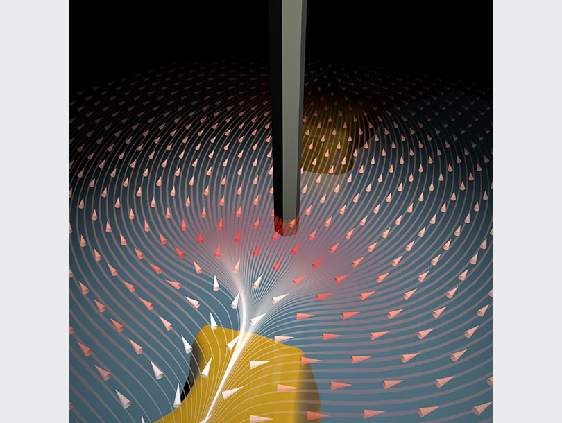
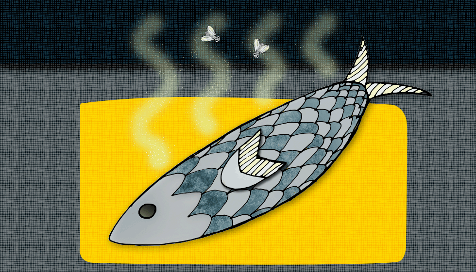
Despite the U.S. Department of Agriculture’s recent goals to drastically reduce food waste, most consumers don’t realize the global problem created by 1.3 billion metric tons of food wasted each year — clogging landfills and releasing unsustainable levels of methane gas into the atmosphere. Using technology developed at MIT’s Swager lab, Cambridge, Ma.-based C2Sense(http://www.c2sense.com/) is developing inexpensive, lightweight hand-held sensors based on carbon nanotubes which can detect fruit ripeness and meat, fish and poultry freshness. Smaller than a half of a business card, these sensors can be developed at very low cost, require very little power to operate, and can be easily integrated into most agricultural supply chains, including food storage packaging, to ensure that food is picked, stored, shipped, and sold at optimal freshness.

“Our mission is to bring a sense of smell to the digital world. With our technology, that package of steaks in your refrigerator will tell you when it’s about to go bad, recommend some recipe options and help build out your shopping list,” said Jan Schnorr, Chief Technology Officer of C2Sense.

Amazing metals that completely repel water

MaxterialTM, Inc. develops amazing materials that resist a variety of detrimental environmental effects through technology that emulates similar strategies found in nature, such as the self-cleaning lotus leaf and antifouling properties of crabs. By modifying the surface shape or texture of a metal, through a method that is very affordable and easy to introduce into the existing manufacturing process, Maxterial introduces a microlayer of air pockets that reduce contact surface area. The underlying material can be chemically the same as ever, retaining inherent properties like thermal and electrical conductivity. But through Maxterial’s technology, the metallic surface also becomes inherently water repellant. This property introduces the superhydrophobic maxterial as a potential solution to a myriad of problems, such as corrosion, biofouling, and ice formation. Maxterial is currently focused on developing durable hygienic and eco-friendly anti-corrosion coatings for metallic surfaces.

“Our process has the potential to create metallic objects that retain their amazing properties for the lifetime of the object – this isn’t an aftermarket coating that can wear or chip off,” said Mehdi Kargar, Co-founder and CEO of Maxterial, Inc. “We are working towards a day when shipping equipment can withstand harsh arctic environments, offshore structures can resist corrosion, and electronics can be fully submersible and continue working as good as new.”

New approaches to combat aging

CyteGen (http://cytegen.com/) wants to dramatically increase the human healthspan, tackle neurodegenerative diseases, and reverse age-related decline. What makes this possible now is new discovery tools backed by the dream team of interdisciplinary experts the company has assembled. CyteGen’s approach is unusually collaborative, tapping into the resources and expertise of world-renowned researchers across eight major universities to focus different strengths and perspectives to achieve the company’s goals. By approaching aging from a holistic, systematic point of view, rather than focusing solely on discrete definitions of disease, they have developed a new way to think about aging, and to develop treatments that can help people live longer, healthier lives.

“There is an assumption that aging necessarily brings the kind of physical and mental decline that results in Parkinson’s, Alzheimer’s, and other diseases. Evidence indicates otherwise, which is what spurred us to launch CyteGen,” said George Ugras, Co-Founder and President of CyteGen.

To date, Breakout Labs has invested in more than two dozen companies at the forefront of science, helping radical technologies get beyond common hurdles faced by early stage companies, and advance research and development to market much more quickly. Portfolio companies have raised more than six times the amount of capital invested in the program by the Thiel Foundation, and represent six Series A valuations ranging from $10 million to $60 million as well as one acquisition.

You can see the original Oct. 6, 2015 Breakout Labs news release here or in this Oct. 7, 2015 news item on Azonano.

Argonne National Labs and Nano Design Works (NDW) and the Argonne Collaborative Center for Energy Storage Science (ACCESS)

The US Department of Energy’s Argonne National Laboratory’s Oct. 6, 2015 press release by Greg Cunningham announced two initiatives meant to speed commercialization of nanotechnology-enabled products for the energy storage and other sectors,

Few technologies hold more potential to positively transform our society than energy storage and nanotechnology. Advances in energy storage research will revolutionize the way the world generates and stores energy, democratizing the delivery of electricity. Grid-level storage can help reduce carbon emissions through the increased adoption of renewable energy and use of electric vehicles while helping bring electricity to developing parts of the world. Nanotechnology has already transformed the electronics industry and is bringing a new set of powerful tools and materials to developers who are changing everything from the way energy is generated, stored and transported to how medicines are delivered and the way chemicals are produced through novel catalytic nanomaterials.

Recognizing the power of these technologies and seeking to accelerate their impact, the U.S. Department of Energy’s Argonne National Laboratory has created two new collaborative centers that provide an innovative pathway for business and industry to access Argonne’s unparalleled scientific resources to address the nation’s energy and national security needs. These centers will help speed discoveries to market to ensure U.S. industry maintains a lead in this global technology race.

“This is an exciting time for us, because we believe this new approach to interacting with business can be a real game changer in two areas of research that are of great importance to Argonne and the world,” said Argonne Director Peter B. Littlewood. “We recognize that delivering to market our breakthrough science in energy storage and nanotechnology can help ensure our work brings the maximum benefit to society.”

Nano Design Works (NDW) and the Argonne Collaborative Center for Energy Storage Science (ACCESS) will provide central points of contact for companies — ranging from large industrial entities to smaller businesses and startups, as well as government agencies — to benefit from Argonne’s world-class expertise, scientific tools and facilities.

NDW and ACCESS represent a new way to collaborate at Argonne, providing a single point of contact for businesses to assemble tailored interdisciplinary teams to address their most challenging R&D questions. The centers will also provide a pathway to Argonne’s fundamental research that is poised for development into practical products. The chance to build on existing scientific discovery is a unique opportunity for businesses in the nano and energy storage fields.

The center directors, Andreas Roelofs of NDW and Jeff Chamberlain of ACCESS, have both created startups in their careers and understand the value that collaboration with a national laboratory can bring to a company trying to innovate in technologically challenging fields of science. While the new centers will work with all sizes of companies, a strong emphasis will be placed on helping small businesses and startups, which are drivers of job creation and receive a large portion of the risk capital in this country.

“For a startup like mine to have the ability to tap the resources of a place like Argonne would have been immensely helpful,” said Roelofs. “We”ve seen the power of that sort of access, and we want to make it available to the companies that need it to drive truly transformative technologies to market.”

Chamberlain said his experience as an energy storage researcher and entrepreneur led him to look for innovative approaches to leveraging the best aspects of private industry and public science. The national laboratory system has a long history of breakthrough science that has worked its way to market, but shortening that journey from basic research to product has become a growing point of emphasis for the national laboratories over the past couple of decades. The idea behind ACCESS and NDW is to make that collaboration even easier and more powerful.

“Where ACCESS and NDW will differ from the conventional approach is through creating an efficient way for a business to build a customized, multi-disciplinary team that can address anything from small technical questions to broad challenges that require massive resources,” Chamberlain said. “That might mean assembling a team with chemists, physicists, computer scientists, materials engineers, imaging experts, or mechanical and electrical engineers; the list goes on and on. It’s that ability to tap the full spectrum of cross-cutting expertise at Argonne that will really make the difference.”

Chamberlain is deeply familiar with the potential of energy storage as a transformational technology, having led the formation of Argonne’s Joint Center for Energy Storage Research (JCESR). The center’s years-long quest to discover technologies beyond lithium-ion batteries has solidified the laboratory’s reputation as one of the key global players in battery research. ACCESS will tap Argonne’s full battery expertise, which extends well beyond JCESR and is dedicated to fulfilling the promise of energy storage.

Energy storage research has profound implications for energy security and national security. Chamberlain points out that approximately 1.3 billion people across the globe do not have access to electricity, with another billion having only sporadic access. Energy storage, coupled with renewable generation like solar, could solve that problem and eliminate the need to build out massive power grids. Batteries also have the potential to create a more secure, stable grid for countries with existing power systems and help fight global climate disruption through adoption of renewable energy and electric vehicles.

Argonne researchers are pursuing hundreds of projects in nanoscience, but some of the more notable include research into targeted drugs that affect only cancerous cells; magnetic nanofibers that can be used to create more powerful and efficient electric motors and generators; and highly efficient water filtration systems that can dramatically reduce the energy requirements for desalination or cleanup of oil spills. Other researchers are working with nanoparticles that create a super-lubricated state and other very-low friction coatings.

“When you think that 30 percent of a car engine’s power is sacrificed to frictional loss, you start to get an idea of the potential of these technologies,” Roelofs said. “But it’s not just about the ideas already at Argonne that can be brought to market, it’s also about the challenges for businesses that need Argonne-level resources. I”m convinced there are many startups out there working on transformational ideas that can greatly benefit from the help of a place Argonne to bring those ideas to fruition. That is what has me excited about ACCESS and NDW.”

For more information on ACCESS, see: access.anl.gov

For more information on NDW, see: nanoworks.anl.gov

You can read more about the announcement in an Oct. 6, 2015 article by Greg Watry for R&D magazine featuring an interview with Andreas Roelofs.

Indian scientists explore graphene ripples

A Sept. 19, 2015 Nanotechnology Now announces that Indian scientists have developed a theory about curved or rippled graphene,

The single-carbon-atom-thick material, graphene, featuring ripples is not easy to understand. Instead of creating such ripples physically, physicists investigating this kind of unusually shaped material rely on a quantum simulator. It is made up of an artificial lattice of light – called ultra-cold optical lattice – akin to eggs held in the cavities of an egg tray. This approach allowed a team of theoretical physicists from India to shed some light – literally and figuratively – on the properties of rippled graphene. These findings have just been published in EPJ B by Tridev Mishra and colleagues from the Birla Institute of Technology and Science, in Pilani, India. Ultimately, this work could find applications in novel graphene-based sensors.

A Sept. 18, 2015 Springer press release, which originated the news item, expands on the theme,

Optical lattices are perfect simulators. They are like mini-laboratories suitable for studying the response of a material after it has been subjected to controllable parameters inducing a deformation. What makes this particular study novel is that the team has managed to control the creation of a curved space or ripples in graphene by relying on an optical lattice simulator. The authors have thus developed a theory describing how a sequence of pulses, whose amplitude can be modulated, changes an optical lattice – specifically, the background geometry of its constituent particles. Previous modelling attempts only described static curved graphene.

Mishra and colleagues have established equations of the energy for particles caught in an optical lattice. This, in turn, simulates the energy of the electrons in a graphene sheet with a curvature. They then use a map to translate the physical characteristics of the approximation used in the curved space picture of graphene to the more realistic optical lattice picture. They thus obtain an understanding of the dynamics of the evolution from the ‘egg in a tray’ structure of the optical lattice in terms of the properties of ‘an omelette style’ continuum of energy found in graphene.

Here’s a link to and a citation for the paper,

Floquet analysis of pulsed Dirac systems: a way to simulate rippled graphene by Tridev Mishra, Tapomoy Guha Sarkar, and Jayendra N. Bandyopadhyaya. Eur. Phys. J. B (2015) 88: 231 http://dx.doi.org/10.1140/epjb/e2015-60356-2 Published online: 16 September 2015

This paper is behind a paywall.

Carbon nanotubes sense spoiled food

CNT_FoodSpolage

Courtesy: MIT (Massachusetts Institute of Technology)

I love this .gif; it says a lot without a word. However for details, you need words and here’s what an April 15, 2015 news item on Nanowerk has to say about the research illustrated by the .gif,

MIT [Massachusetts Institute of Technology] chemists have devised an inexpensive, portable sensor that can detect gases emitted by rotting meat, allowing consumers to determine whether the meat in their grocery store or refrigerator is safe to eat.

The sensor, which consists of chemically modified carbon nanotubes, could be deployed in “smart packaging” that would offer much more accurate safety information than the expiration date on the package, says Timothy Swager, the John D. MacArthur Professor of Chemistry at MIT.

An April 14, 2015 MIT news release (also on EurekAlert), which originated the news item, offers more from Dr. Swager,

It could also cut down on food waste, he adds. “People are constantly throwing things out that probably aren’t bad,” says Swager, who is the senior author of a paper describing the new sensor this week in the journal Angewandte Chemie.

This latest study is builds on previous work at Swager’s lab (Note: Links have been removed),

The sensor is similar to other carbon nanotube devices that Swager’s lab has developed in recent years, including one that detects the ripeness of fruit. All of these devices work on the same principle: Carbon nanotubes can be chemically modified so that their ability to carry an electric current changes in the presence of a particular gas.

In this case, the researchers modified the carbon nanotubes with metal-containing compounds called metalloporphyrins, which contain a central metal atom bound to several nitrogen-containing rings. Hemoglobin, which carries oxygen in the blood, is a metalloporphyrin with iron as the central atom.

For this sensor, the researchers used a metalloporphyrin with cobalt at its center. Metalloporphyrins are very good at binding to nitrogen-containing compounds called amines. Of particular interest to the researchers were the so-called biogenic amines, such as putrescine and cadaverine, which are produced by decaying meat.

When the cobalt-containing porphyrin binds to any of these amines, it increases the electrical resistance of the carbon nanotube, which can be easily measured.

“We use these porphyrins to fabricate a very simple device where we apply a potential across the device and then monitor the current. When the device encounters amines, which are markers of decaying meat, the current of the device will become lower,” Liu says.

In this study, the researchers tested the sensor on four types of meat: pork, chicken, cod, and salmon. They found that when refrigerated, all four types stayed fresh over four days. Left unrefrigerated, the samples all decayed, but at varying rates.

There are other sensors that can detect the signs of decaying meat, but they are usually large and expensive instruments that require expertise to operate. “The advantage we have is these are the cheapest, smallest, easiest-to-manufacture sensors,” Swager says.

“There are several potential advantages in having an inexpensive sensor for measuring, in real time, the freshness of meat and fish products, including preventing foodborne illness, increasing overall customer satisfaction, and reducing food waste at grocery stores and in consumers’ homes,” says Roberto Forloni, a senior science fellow at Sealed Air, a major supplier of food packaging, who was not part of the research team.

The new device also requires very little power and could be incorporated into a wireless platform Swager’s lab recently developed that allows a regular smartphone to read output from carbon nanotube sensors such as this one.

The funding sources are interesting, as I am appreciating with increasing frequency these days (from the news release),

The researchers have filed for a patent on the technology and hope to license it for commercial development. The research was funded by the National Science Foundation and the Army Research Office through MIT’s Institute for Soldier Nanotechnologies.

Here’s a link to and a citation for the paper,

Single-Walled Carbon Nanotube/Metalloporphyrin Composites for the Chemiresistive Detection of Amines and Meat Spoilage by Sophie F. Liu, Alexander R. Petty, Dr. Graham T. Sazama, and Timothy M. Swager. Angewandte Chemie International Edition DOI: 10.1002/anie.201501434 Article first published online: 13 APR 2015

© 2015 WILEY-VCH Verlag GmbH & Co. KGaA, Weinheim

This article is behind a paywall.

There are other posts here about the quest to create food sensors including this Sept. 26, 2013 piece which features a critique (by another blogger) about trying to create food sensors that may be more expensive than the item they are protecting, a problem Swager claims to have overcome in an April 17, 2015 article by Ben Schiller for Fast Company (Note: Links have been removed),

Swager has set up a company to commercialize the technology and he expects to do the first demonstrations to interested clients this summer. The first applications are likely to be for food workers working with meat and fish, but there’s no reason why consumers shouldn’t get their own devices in due time.

There are efforts to create visual clues for food status. But Swager says his method is better because it doesn’t rely on perception: it produces hard data that can be logged and tracked. And it also has potential to be very cheap.

“The resistance method is a game-changer because it’s two to three orders of magnitude cheaper than other technology. It’s hard to imagine doing this cheaper,” he says.