Tag Archives: Shrinky Dinks

A new Shrinky Dinks story: super-wrinkled and super-crumpled graphene for self-cleaning surfaces and other applications

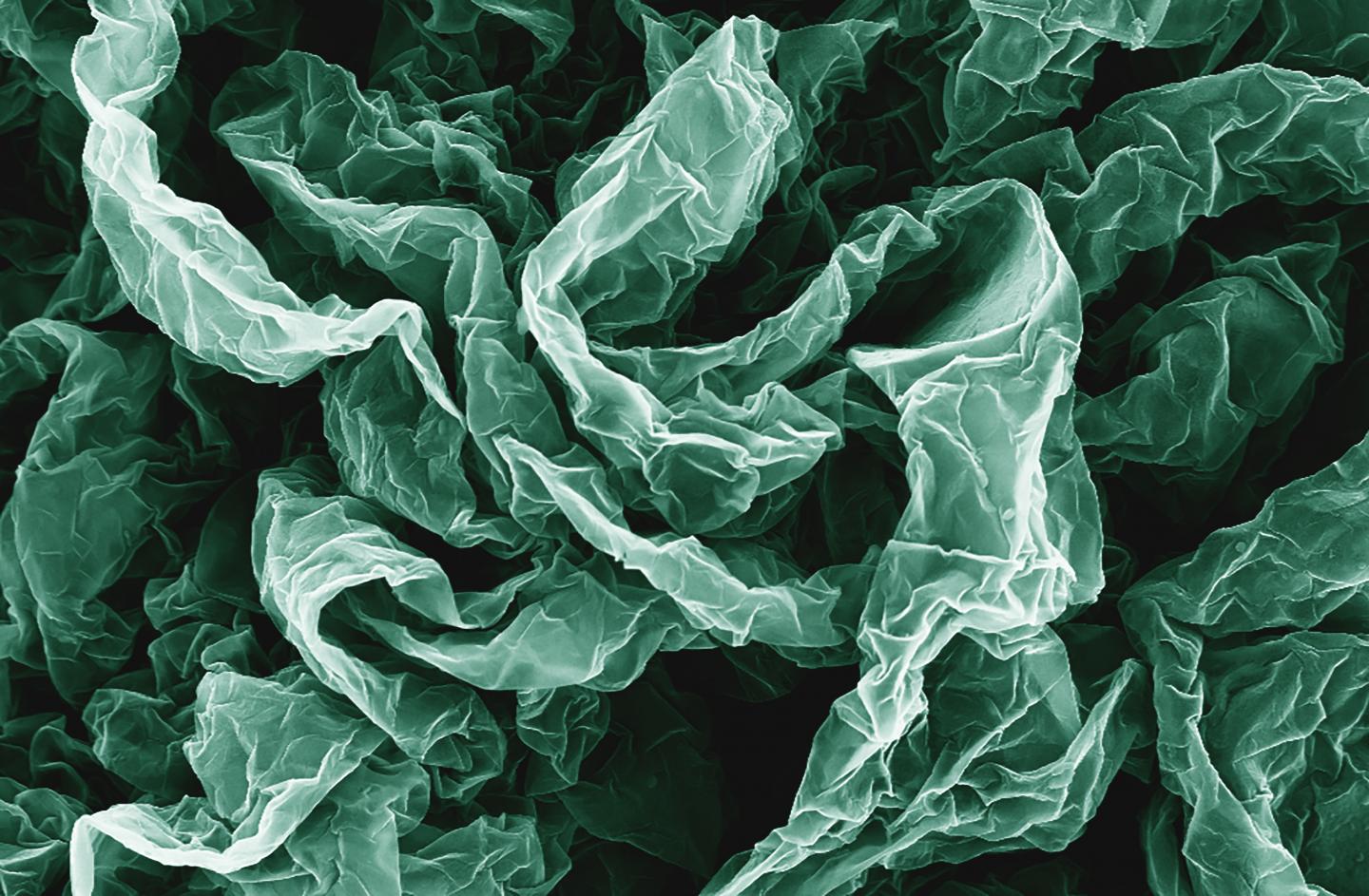
Caption: Wrinkles and crumples, introduced by placing graphene on shrinky polymers, can enhance graphene's properties. Credit: Hurt and Wong Labs / Brown University

Caption: Wrinkles and crumples, introduced by placing graphene on shrinky polymers, can enhance graphene’s properties. Credit: Hurt and Wong Labs / Brown University

A March 21, 2016 news item on ScienceDaily describes how Brown University (US) researchers developed super-wrinkled and super-crumpled graphene,

Crumple a piece of paper and it’s probably destined for the trash can, but new research shows that repeatedly crumpling sheets of the nanomaterial graphene can actually enhance some of its properties. In some cases, the more crumpled the better.

The research by engineers from Brown University shows that graphene, wrinkled and crumpled in a multi-step process, becomes significantly better at repelling water–a property that could be useful in making self-cleaning surfaces. Crumpled graphene also has enhanced electrochemical properties, which could make it more useful as electrodes in batteries and fuel cells.

A March 21, 2016 Brown University news release (also on EurekAlert), which originated the news item, provides more detail about the current and previous research,

This new research builds on previous work done by Robert Hurt and Ian Wong, from Brown’s School of Engineering. The team had previously showed that by introducing wrinkles into graphene, they could make substrates for culturing cells that were more similar to the complex environments in which cells grow in the body. For this latest work, the researchers led by Po-Yen Chen, a Hibbit postdoctoral fellow, wanted to build more complex architectures incorporating both wrinkles and crumples. “I wanted to see if there was a way to create higher-generational structures,” Chen said.

To do that, the researchers deposited layers of graphene oxide onto shrink films–polymer membranes that shrink when heated (kids may know these as Shrinky Dinks [emphasis mine]). As the films shrink, the graphene on top is compressed, causing it to wrinkle and crumple. To see what kind of structures they could create, the researchers compressed same graphene sheets multiple times. After the first shrink, the film was dissolved away, and the graphene was placed in a new film to be shrunk again.

The researchers experimented with different configurations in the successive generations of shrinking. For example, sometimes they clamped opposite ends of the films, which caused them to shrink only along one axis. Clamped films yielded graphene sheets with periodic, basically parallel wrinkles across its surface. Unclamped films shrank in two dimensions, both length- and width-wise, creating a graphene surface that was crumpled in random shapes.

The team experimented with those different modes of shrinking over three successive generations. For example, they might shrink the same graphene sheet on a clamped film, then an unclamped film, then clamped again; or unclamped, clamped, unclamped. They also rotated the graphene in different configurations between shrinkings, sometimes placing the sheet perpendicular to its original orientation.

The team found that the multi-generational approach could substantially compress the graphene sheets, making them as small as one-fortieth their original size. They also showed that successive generations could create interesting patterns along the surface–wrinkles and crumples that were superimposed onto each other, for example.

“As you go deeper into the generations you tend to get larger wavelength structures with the original, smaller wavelength structure from earlier generations built into them,” said Robert Hurt, a professor of engineering at Brown and one of the paper’s corresponding authors.

A sheet that was shrunk clamped, unclamped, and then clamped looked different from ones that were unclamped, clamped, unclamped, for example.

“The sequence matters,” said Wong, also a corresponding author on the paper. “It’s not like multiplication where 2 times 3 is the same as 3 times 2. The material has a ‘memory’ and we get different results when we wrinkle or crumple in a different order.”

The researchers generated a kind of taxonomy of structures born from different shrinking configurations. They then tested several of those structures to see how they altered the properties of the graphene sheets.

Enhanced properties

They showed that a highly crumpled graphene surface becomes superhydrophobic–able to resist wetting by water. When water touches a hydrophobic surface, it beads up and rolls off. When the contact angle of those water beads with an underlying surface exceeds 160 degrees–meaning very little of the water bead’s surface touches the material–the material is said to be superhydrophobic. The researchers showed that they could make superhydrophobic graphene with three unclamped shrinks.

The team also showed that crumpling could enhance the electrochemical behaviors of graphene, which could be useful in next-generation energy storage and generation. The research showed that crumpled graphene used as a battery electrode had as much as a 400 percent increase in electrochemical current density over flat graphene sheets. That increase in current density could make for vastly more efficient batteries.

“You don’t need a new material to do it,” Chen said. “You just need to crumple the graphene.”

In additional to batteries and water resistant coatings, graphene compressed in this manner might also be useful in stretchable electronics–a wearable sensor, for example.

The group plans to continue experimenting with different ways of generating structures on graphene and other nanomaterials.

“There are many new two-dimensional nanomaterials that have interesting properties, not just graphene,” Wong said. “So other materials or combinations of materials may also organize into interesting structures with unexpected functionalities.”

Here’s a link to and a citation for the paper,

Multiscale Graphene Topographies Programmed by Sequential Mechanical Deformation by Po-Yen Chen, Jaskiranjeet Sodhi, Yang Qiu, Thomas M. Valentin, Ruben Spitz Steinberg, Zhongying Wang, Robert H. Hurt, and Ian Y. Wong. Advanced Materials DOI: 10.1002/adma.201506194 Article first published online: 21 MAR 2016

© 2016 WILEY-VCH Verlag GmbH & Co. KGaA, Weinheim

This paper is behind a paywall.

As for Shrinky Dinks, I first featured this material and its use in science research in an Aug. 16, 2010 posting about Shrinky Dinks and nanopatterning. It was originally developed by Betty J. Morris as craft material for children. Both she and the scientist kindly answered some followup questions inspired by the original news release and published in the 2010 post.

Shrinky Dinks* instrumental for new nanowires technique

Shrinky Dinks, a material used for children’s arts and crafts projects, has proved instrumental for developing a new technique to close the gap between nanowires. From a July 1, 2014 news item on Nanowerk (Note: A link has been removed),

How do you put a puzzle together when the pieces are too tiny to pick up? Shrink the distance between them.

Engineers at the University of Illinois at Urbana-Champaign are using Shrinky Dinks, plastic that shrinks under high heat, to close the gap between nanowires in an array to make them useful for high-performance electronics applications. The group published its technique in the journal Nano Letters (“Assembly and Densification of Nanowire Arrays via Shrinkage”).

A July 1, 2014 University of Illinois at Urbana-Champaign news release, which originated the news item, provides more details about the new technique,

Nanowires are extremely fast, efficient semiconductors, but to be useful for electronics applications, they need to be packed together in dense arrays. Researchers have struggled to find a way to put large numbers of nanowires together so that they are aligned in the same direction and only one layer thick.

“Chemists have already done a brilliant job in making nanowires exhibit very high performance. We just don’t have a way to put them into a material that we can handle,” said study leader SungWoo Nam, a professor of mechanical science and engineering at the U. of I. “With the shrinking approach, people can make nanowires and nanotubes using any method they like and use the shrinking action to compact them into a higher density.”

The researchers place the nanowires on the Shrinky Dinks plastic as they would for any other substrate, but then shrink it to bring the wires much closer together. This allows them to create very dense arrays of nanowires in a simple, flexible and very controllable way.

The shrinking method has the added bonus of bringing the nanowires into alignment as they increase in density. Nam’s group demonstrated how even wires more than 30 degrees off-kilter can be brought into perfect alignment with their neighbors after shrinking.

“There’s assembly happening at the same time as the density increases,” Nam said, “so even if the wires are assembled in a disoriented direction we can still use this approach.”

The plastic is clamped before baking so that it only shrinks in one direction, so that the wires pack together but do not buckle. Clamping in different places could direct the arrays into interesting formations, according to Nam. The researchers also can control how densely the wires pack by varying the length of time the plastic is heated. They also are exploring using lasers to precisely shrink the plastic in specific patterns.

Nam first had the idea for using Shrinky Dinks plastic to assemble nanomaterials after seeing a microfluidics device that used channels made of shrinking plastic. He realized that the high degree of shrinking and the low cost of plastic could have a huge impact on nanowire assembly and processing for applications.

“I’m interested in this concept of synthesizing new materials that are assembled from nanoscale building blocks,” Nam said. “You can create new functions. For example, experiments have shown that film made of packed nanowires has properties that differ quite a bit from a crystal thin film.”

One application the group is now exploring is a thin film solar cell, made of densely packed nanowires, that could harvest energy from light much more efficiently than traditional thin-film solar cells.

I have featured the Shrinky Dinks product and its use for nanoscale fabrication before in an Aug. 16, 2010 posting which featured this reply from the lead researcher for that project on nanopatterning,

ETA Aug.17.10: I also contacted Teri W. Odom, professor at Northwestern University about why they use Slinky Dinks in their work. She very kindly responded with this:

Part of what we are interested in is the development of low-cost nanofabrication tools that can create macroscale areas of nanoscale patterns in a single step. For a variety of reasons, this end-product is hard to obtain—even though we and others have chipped away at this problem for years.

As an example, to achieve smaller and smaller separations between patterns, either expensive, top-down serial tools (such as electron beam lithography or scanning probe techniques) or bottom-up assembly methods need to be used. However, the former cannot easily create large areas of patterns, and the latter cannot readily control the separations of patterns.

We needed a way to obtain nanopatterns separated by specific distances on-demand. Here is where the Shrinky Dinks material comes in. My student had read a paper (published in 2007 in Lab on a Chip) about how this material was used to make microscale patterns starting from a pattern printed using a laser printer. I imagine his thought was: if this material could be used for microscale patterns, why not for nanoscale ones? It would be cheap, and it’s easy to order.

So, we combined this substrate with our new molding method—solvent assisted nanoscale embossing (SANE)—and could now heat the material to shrink the spacing between patterns. And thus, in some sense, we made available to any lab some of the capabilities of the billion-dollar nanofabrication industry for less than one-hundred dollars.

Getting back to this latest use of Shrinky Dinks, here’s a link to and a citation for the ‘nanowires’ research paper,

Assembly and Densification of Nanowire Arrays via Shrinkage by Jaehoon Bang, Jonghyun Choi, Fan Xia, Sun Sang Kwon, Ali Ashraf, Won Il Park, and SungWoo Nam. Nano Lett., 2014, 14 (6), pp 3304–3308 DOI: 10.1021/nl500709p Publication Date (Web): May 16, 2014
Copyright © 2014 American Chemical Society

This paper is behind a paywall.

* ‘dinks’ in headline changed to ‘Dinks’ on July 2, 2014 at 1150 hours PDT.

Nano crafts class: get out your ‘paper’ and scissors

It’s not all atomic force microscopy and nanotweezers as scientists keep reminding us that the techniques we learned in kindergarten can be all the high technology we need even when working at the nanoscale. From the Nov. 14, 2012 news item on ScienceDaily,

Two Northwestern University researchers have discovered a remarkably easy way to make nanofluidic devices: using paper and scissors. And they can cut a device into any shape and size they want, adding to the method’s versatility.

The Nov. 14, 2012 Northwestern University news release by Megan Fellman explains both nanofluidic devices and the new technique,

Nanofluidic devices are attractive because their thin channels can transport ions — and with them a higher than normal electric current — making the devices promising for use in batteries and new systems for water purification, harvesting energy and DNA sorting.

The “paper-and-scissors” method one day could be used to manufacture large-scale nanofluidic devices without relying on expensive lithography techniques.

The Northwestern duo found that simply stacking up sheets of the inexpensive material graphene oxide creates flexible “paper” with tens of thousands of very useful channels. A tiny gap forms naturally between neighboring sheets, and each gap is a channel through which ions can flow.

Using a pair of regular scissors, the researchers simply cut the paper into a desired shape, which, in the case of their experiments, was a rectangle.

“In a way, we were surprised that these nanochannels actually worked, because creating the device was so easy,” said Jiaxing Huang, who conducted the research with postdoctoral fellow Kalyan Raidongia. “No one had thought about the space between sheet-like materials before. Using the space as a flow channel was a wild idea. We ran our experiment at least 10 times to be sure we were right.”

The process is a little more complex than kindergarten crafts (from Fellman’s news release),

To create a working device, the researchers took a pair of scissors and cut a piece of their graphene oxide paper into a centimeter-long rectangle. They then encased the paper in a polymer, drilled holes to expose the ends of the rectangular piece and filled up the holes with an electrolyte solution (a liquid containing ions) to complete the device.

Next they put electrodes at both ends and tested the electrical conductivity of the device. Huang and Raidongia observed higher than normal current, and the device worked whether flat or bent.

The nanochannels have significantly different — and desirable — properties from their bulk channel counterparts, Huang said. The nanochannels have a concentrating effect, resulting in an electric current much higher than those in bulk solutions.

Graphene oxide is basically graphene sheets decorated with oxygen-containing groups. It is made from inexpensive graphite powders by chemical reactions known for more than a century.

Scaling up the size of the device is simple. Tens of thousands of sheets or layers create tens of thousands of nanochannels, each channel approximately one nanometer high. There is no limit to the number of layers — and thus channels — one can have in a piece of paper.

To manufacture very massive arrays of channels, one only needs to put more graphene oxide sheets in the paper or to stack up many pieces of paper. A larger device, of course, can handle larger quantities of electrolyte.

Kindergarten techniques worked well for Andre Geim and Konstantin Novoselov who received Nobel prizes for their work on graphene (from my Oct. 7,2010 posting),

The technique that Geim and Novoselov used to create the first graphene sheets both amuses and fascinates me (from the article by Kit Eaton on the Fast Company website),

The two scientists came up with the technique that first resulted in samples of graphene–peeling individual atoms-deep sheets of the material from a bigger block of pure graphite. The science here seems almost foolishly simple, but it took a lot of lateral thinking to dream up, and then some serious science to investigate: Geim and Novoselo literally “ripped” single sheets off the graphite by using regular adhesive tape.

Then, there’s the ‘Shrinky Dinks’ nanopatterning technique (from my Aug. 16,2010 posting),

Scientists at a Northwestern University laboratory have taken to using a children’s arts and crafts product, Shrinky Dinks, for a new way to create large area nanoscale patterns on the cheap.

It’s good to be reminded that science at its heart is not about expensive equipment and complicated techniques but a means of exploring the world around us with the means at hand.

Graphene, the Nobel Prize, and levitating frogs

As you may have heard, two  scientists (Andre Geim and Konstantin Novoselov) who performed groundbreaking research on graphene [Nov. 29, 2010: I corrected this entry Nov. 26, 2010 which originally stated that these researchers discovered graphene] have been awarded the 2010 Nobel Prize for Physics. In honour of their award, the journal, Nature Materials, is giving free access to  a 2007 article authored by the scientists. From the news item on Nanowerk,

The 2007 landmark article in Nature Materials “The rise of graphene” by the just announced winners of the 2010 Nobel prize in physics, Andre Geim and Kosta Novoselov, has now been made available as a free access article.

Abstract:

Graphene is a rapidly rising star on the horizon of materials science and condensed-matter physics. This strictly two-dimensional material exhibits exceptionally high crystal and electronic quality, and, despite its short history, has already revealed a cornucopia of new physics and potential applications, which are briefly discussed here.

Here’s a description of the scientists and their work from the BBC News article by Paul Rincon,

Prof Geim, 51, is a Dutch national while Dr Novoselov, 36, holds British and Russian citizenship. Both are natives of Russia and started their careers in physics there.

The Nobels are valued at 10m Swedish kronor (£900,000; 1m euros; $1.5m).

They first worked together in the Netherlands before moving to the UK. They were based at the University of Manchester when they published their groundbreaking research paper on graphene in October 2004.

Dr Novoselov is among the youngest winners of a prize that normally goes to scientists with decades of experience.

Graphene is a form of carbon. It is a flat layer of carbon atoms tightly packed into a two-dimensional honeycomb arrangement.

Because it is so thin, it is also practically transparent. As a conductor of electricity it performs as well as copper, and as a conductor of heat it outperforms all other known materials.

The unusual electronic, mechanical and chemical properties of graphene at the molecular scale promise ultra-fast transistors for electronics.

Some scientists have predicted that graphene could one day replace silicon – which is the current material of choice for transistors.

It could also yield incredibly strong, flexible and stable materials and find applications in transparent touch screens or solar cells.

Geim and Novoselov first isolated fine sheets of graphene from the graphite which is widely used in pencils.

A layer of graphite 1mm thick actually consists of three million layers of graphene stacked on top of one another.

The technique that Geim and Novoselov used to create the first graphene sheets both amuses and fascinates me (from the article by Kit Eaton on the Fast Company website),

The two scientists came up with the technique that first resulted in samples of graphene–peeling individual atoms-deep sheets of the material from a bigger block of pure graphite. The science here seems almost foolishly simple, but it took a lot of lateral thinking to dream up, and then some serious science to investigate: Geim and Novoselo literally “ripped” single sheets off the graphite by using regular adhesive tape. Once they’d confirmed they had grabbed micro-flakes of the material, Geim and Novoselo were responsible for some of the very early experiments into the material’s properties. Novel stuff indeed, but perhaps not so unexpected from a scientist (Geim) who the Nobel Committe notes once managed to make a frog levitate in a magnetic field.

I’ll get to the levitating frog in a minute but first the bit about using regular adhesive tape to peel off single sheets only atoms thick of graphite from a larger block of the stuff reminds me of how scientists at Northwestern University are using shrinky dinks (a child’s craft material) to create large scale nanopatterns cheaply (my Aug. 16, 2010 posting).

It’s reassuring to me that despite all of the high tech equipment that costs the earth, scientists still use fairly mundane, inexpensive objects to do some incredibly sophisticated work. The other thing I find reassuring is that Novoselov probably was not voted ‘most likely to be awarded a Nobel Prize’. Interestingly, Novoselov’s partner, Geim, was not welcomed into a physics career with open arms. From the news item on physoorg.com,

Konstantin Novoselov, the Russian-born physicist who shared this year’s Nobel prize, struggled with physics as a student and was awarded a handful of B grades, his university said Wednesday.

The Moscow Physics and Technology University (MFTI) posted report cards on its website for Novoselov, who at 36 won the Nobel prize for physics with his research partner Andre Geim.

The reports reveal that he gained a handful of B grades in his term reports for theoretical and applied physics from 1991 to 1994.

He was also not strong on physical education — a compulsory subject at Russian universities — gaining B grades. And while he now lives in Britain, he once gained a C grade for English.

The university also revealed documents on Nobel prize winner Geim, who studied at the same university from 1976 to 1982. His brilliant academic career was only marred by a few B-grades for Marxist political economy and English.

Geim was turned down when he applied first to another Moscow university specialising in engineering and physics, and worked as a machinist at a factory making electrical instruments for eight months.

Given the increasing emphasis on marks, in Canadian universities at least, I noticed that Novoselov was not a straight-A student. As for Geim, it seems the fact that his father was German posed a problem. (You can find more details in the physorg.com article.)

As for levitating frogs, I first found this information in particle physicist Jon Butterworth’s October 5, 2010 posting on his Guardian blog,

Geim is also well known (or as his web page puts it “notorious”) for levitating frogs. This is a demonstration of the peculiar fact that all materials have some magnetism, albeit very weak in most cases, and that if you put them in a high enough magnetic field you can see the effects – and make them fly.

Why frogs? Well, no frogs were harmed in the experiments. But also, magnetism is a hugely important topic in physics that can seem a little dry to students …

I hunted down a video of the levitating frog on youtube,

As a particle physicist, Butterworth notes that the graphene work is outside his area of expertise so if you’re looking for a good, general explanation with some science detail added in for good measure, I’d suggest reading his succinct description.

Using Shrinky Dinks for SANE nanopatterning

I’m charmed. Scientists at a Northwestern University laboratory have taken to using a children’s arts and crafts product, Shrinky Dinks, for a new way to create large area nanoscale patterns on the cheap. First, something more about the Shrinky Dinks (from their website),

We are the Originators and Manufacturers of SHRINKY DINKS shrinkable plastics.

The very first SHRINKY DINKS were sold on October 17, 1973 at Brookfield Square Shopping Mall in Brookfield Wisconsin. Since that time there has been over 250 different Toy Activity and Craft Kits created and marketed.

SHRINKY DINKS SHRINK to approximately 1/3rd their original size and actually become 9 times thicker. Simply place the SHRINKY DINKS piece you created into a Home Oven or Toaster Oven for 2 magic minutes. Watch as your creation gets smaller and smaller.

It’s “MAGICAL” and it’s so quick and easy to do!

There’s also a video (sadly I can’t embed it here)  about the origins, some very simple science, and ideas on how to use Shrinky Dinks.

As for the scientists, there’s no word on how they decided to use this  product for their work (from the news item on physorg.com),

“Anyone needing access to large-area nanoscale patterns on the cheap could benefit from this method,” said Teri W. Odom, associate professor of chemistry and Dow Chemical Company Research Professor in the Weinberg College of Arts and Sciences. Odom led the research. “It is a simple, low-cost and high-throughput nanopatterning method that can be done in any laboratory.”

Details of the solvent-assisted nanoscale embossing (SANE) method are published by the journal Nano Letters. The work also will appear as the cover story of the journal’s February 2011 issue.

The method offers unprecedented opportunities to manipulate the electronic, photonic and magnetic properties of nanomaterials. It also easily controls a pattern’s size and symmetry and can be used to produce millions of copies of the pattern over a large area. Potential applications include devices that take advantage of nanoscale patterns, such as solar cells, high-density displays, computers and chemical and biological sensors.

“No other existing nanopatterning method can both prototype arbitrary patterns with small separations and reproduce them over six-inch wafers for less than $100,” Odom said.

ETA Aug. 17, 2010: I emailed the originator of Shrinky Dinks, Betty J. Morris asking her how she came up with the name for her product yesterday. Here is her very kind reply,

You were wondering how we came up with the name Shrinky Dinks…To be honest, we were trying to come up with a name that would describe the process…the pieces “shrink” and they become “small”… what are words that mean small…one of the words we came up with was “dinky”…we thought of Shrink Dinky…Shrink Dinkies…Shrinkie Dinkies but ultimately liked the sound of Shrinky Dinks…it was just trying out different words that we thought might be unique and worthy of getting a Trademark…our product has now been on the market 37 years…we have Shrinky Dinks Trademarks in 42 different countries and there have been over 250 different SD kits created and marketed over the years…who would have ever imagined such a success story… not me…that’s for sure!

The story reminds me of how one writes a poem, playing with words.  As Betty says it is a remarkable story and, for me, the science (nanopaterning)/kid’s play (Shrinky Dinks) connection is the best part.

ETA Aug.17.10: I also contacted Teri W. Odom, professor at Northwestern University about why they use Slinky Dinks in their work. She very kindly responded with this:

Part of what we are interested in is the development of low-cost nanofabrication tools that can create macroscale areas of nanoscale patterns in a single step. For a variety of reasons, this end-product is hard to obtain—even though we and others have chipped away at this problem for years.

As an example, to achieve smaller and smaller separations between patterns, either expensive, top-down serial tools (such as electron beam lithography or scanning probe techniques) or bottom-up assembly methods need to be used. However, the former cannot easily create large areas of patterns, and the latter cannot readily control the separations of patterns.

We needed a way to obtain nanopatterns separated by specific distances on-demand. Here is where the Shrinky Dinks material comes in. My student had read a paper (published in 2007 in Lab on a Chip) about how this material was used to make microscale patterns starting from a pattern printed using a laser printer. I imagine his thought was: if this material could be used for microscale patterns, why not for nanoscale ones? It would be cheap, and it’s easy to order.

So, we combined this substrate with our new molding method—solvent assisted nanoscale embossing (SANE)—and could now heat the material to shrink the spacing between patterns. And thus, in some sense, we made available to any lab some of the capabilities of the billion-dollar nanofabrication industry for less than one-hundred dollars.

There is something pleasing about using an everyday, inexpensive product for high end technology. Brava!

ETA Aug.23.10: Michael Berger has written an in depth article at Nanoterk on this type of nanofabrication which includes an interview with Teri Odom.