Tag Archives: silane

Desalination with nanowood

A new treatment for wood could make renewable salt-separating membranes. Courtesy: University of Maryland

An August 6, 2019 article by Adele Peters for Fast Company describes a ‘wooden’approach to water desalinization (also known as desalination),

“We are trying to develop a new type of membrane material that is nature-based,” says Z. Jason Ren, an engineering professor at Princeton University and one of the coauthors of a new paper in Science Advances about that material, which is made from wood. It’s designed for use in a process called membrane distillation, which heats up saltwater and uses pressure to force the water vapor through a membrane, leaving the salt behind and creating pure water. The membranes are usually made from a type of plastic. Using “nanowood” membranes instead can both improve the energy efficiency of the process and avoid the environmental problems of plastic.

An August 2, 2019 University of Maryland (UMD) news release provides more detail about the research,

A membrane made of a sliver of wood could be the answer to renewably sourced water cleaning. Most membranes that are currently used to distill fresh water from salty are made of polymers based on fossil fuels.

Inspired by the intricate system of water circulating in a tree, a research team from the University of Maryland, Princeton University, and the University of Colorado Boulder have figured out how to use a thin slice of wood as a membrane through which water vapor can evaporate, leaving behind salt or other contaminants.

“This work demonstrates another exciting energy/water application of nanostructured wood, as a high-performance membrane material,” said Liangbing Hu, a professor of materials science and engineering at UMD’s A. James Clark School of Engineering, who co-led the study.

The team chemically treated the wood to become hydrophobic, so that it more efficiently allows water vapor through, driven by a heat source like solar energy.

“This study discovered a new way of using wood materials’ unique properties as both an excellent insulator and water vapor transporter,” said Z. Jason Ren, a professor in environmental engineering who recently moved from CU Boulder to Princeton, and the other co-leader of the team that performed the study.

The researchers treat the wood so that it loses its lignin, the part of the wood that makes it brown and rigid, and its hemicellulose, which weaves in and out between cellulose to hold it in place. The resulting “nanowood” is treated with silane, a compound used to make silicon for computer chips. The semiconducting nature of the compound maintains the wood’s natural nanostructures of cellulose, and clings less to water vapor molecules as they pass through. Silane is also used in solar cell manufacturing.

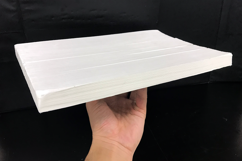
The membrane looks like a thin piece of wood, seemingly bleached white, that is suspended above a source of water vapor. As the water heats and passes into the gas phase, the molecules are small enough to fit through the tiny channels lining the walls of the leftover cell structure. Water collected on the other side is now free of large contaminants like salt.
To test it, the researchers distilled water through it and found that it performed 1.2 times better than a conventional membrane.

“The wood membrane has very high porosity, which promotes water vapor transport and prevents heat loss,” said first author Dianxun Hou, who was a student at CU Boulder.
Inventwood, a UMD spinoff company of Hu’s research group, is working on commercializing wood based nanotechnologies.

Here’s a link to and a citation for the paper,

Hydrophobic nanostructured wood membrane for thermally efficient distillation by Dianxun Hou, Tian Li, Xi Chen, Shuaiming He, Jiaqi Dai, Sohrab A. Mofid, Deyin Hou, Arpita Iddya, David Jassby, Ronggui Yang, Liangbing Hu, and Zhiyong Jason Ren. Science Advances 02 Aug 2019: Vol. 5, no. 8, eaaw3203 DOI: 10.1126/sciadv.aaw3203

This paper appears to be open access.

In my brief survey of the paper, I noticed that the researchers were working with cellulose nanofibrils (CNF), a term which should be familiar for anyone following the nanocellulose story, such as it.

E-ink discovery could be a gateway to cheaper solar cells and electronic touch pads

Non-toxic, inexpensive, and durable are words which, in combination, seem downright magical and all are mentioned in a July 31, 2013 news item on Azonano,

Researchers in the University of Minnesota’s College of Science and Engineering and the National Renewable Energy Laboratory in Golden, Colo., have overcome technical hurdles in the quest for inexpensive, durable electronics and solar cells made with non-toxic chemicals. …

“Imagine a world where every child in a developing country could learn reading and math from a touch pad that costs less than $10 or home solar cells that finally cost less than fossil fuels,” said Uwe Kortshagen, a University of Minnesota mechanical engineering professor and one of the co-authors of the paper.

The July 30, 2013 University of Minnesota news release, which originated the news item, explains the discovery and the issues the researchers are addressing and it mentions, as many do these days,  a patent,

The research team discovered a novel technology to produce a specialized type of ink from non-toxic nanometer-sized crystals of silicon, often called “electronic ink.” This “electronic ink” could produce inexpensive electronic devices with techniques that essentially print it onto inexpensive sheets of plastic.

“This process for producing electronics is almost like screen printing a number on a softball jersey,” said Lance Wheeler, a University of Minnesota mechanical engineering Ph.D. student and lead author of the research.

But it’s not quite that easy. Wheeler, Kortshagen and the rest of the research team developed a method to solve fundamental problems of silicon electronic inks.

First, there is the ubiquitous need of organic “soap-like” molecules, called ligands, that are needed to produce inks with a good shelf life, but these molecules cause detrimental residues in the films after printing. This leads to films with electrical properties too poor for electronic devices. Second, nanoparticles are often deliberately implanted with impurities, a process called “doping,” to enhance their electrical properties.

In this new paper, researchers explain a new method to use an ionized gas, called nonthermal plasma, to not only produce silicon nanocrystals, but also to cover their surfaces with a layer of chlorine atoms. This surface layer of chlorine induces an interaction with many widely used solvents that allows production of stable silicon inks with excellent shelf life without the need for organic ligand molecules. In addition, the researchers discovered that these solvents lead to doping of films printed from their silicon inks, which gave them an electrical conductivity 1,000 times larger than un-doped silicon nanoparticle films. The researchers have a provisional patent on their findings.

Here’s a link to and a citation for the published paper,

Hypervalent surface interactions for colloidal stability and doping of silicon nanocrystals by Lance M. Wheeler, Nathan R. Neale, Ting Chen, & Uwe R. Kortshagen. Nature Communications 4, Article number: 2197 doi:10.1038/ncomms3197 Published 29 July 2013

The paper is open access. The researchers also offer a brief video describing the process of making the nanocrystals,

Here’s the video description provided by the researchers (from http://www.youtube.com/watch?v=5Un_HnOl6lQ&feature=youtu.be),

This video shows how silicon nanocrystals are synthesized in a plasma reactor. Inert argon gas flows from the top of the reactor through a glass tube. Fifteen watts of radio frequency power is applied to the copper ring electrodes to ionize the argon gas and produce what is called a plasma. A gas containing silicon (silane) is injected into the reactive plasma environment to produce silicon nanocrystals. Though the plasma is energetic enough to produce these tiny crystals, the glass tube remains cool enough to touch. The plasma is a reactive environment used to produce silicon nanocrystals that can be applied to inexpensive, next-generation electronics.