Tag Archives: silicene

Silicene in Saskatchewan (Canada)

There’s some very exciting news coming out of the province of Saskatchewan (Canada) about silicene, a material some view as a possible rival to graphene (although that’s problematic according to my Jan. 12, 2014 posting) while others (US National Argonne Laboratory) challenge its existence (my Aug. 1,  2014 posting).

The researchers in Saskatchewan seem quite confident in silicene’s existence according to a Sept. 9, 2014 news item on phys.org,

“Once a device becomes too small it falls prey to the strange laws of the quantum world,” says University of Saskatchewan researcher Neil Johnson, who is using the Canadian Light Source synchrotron to help develop the next generation of computer materials. Johnson is a member of Canada Research Chair Alexander Moewes’ group of graduate students studying the nature of materials using synchrotron radiation.

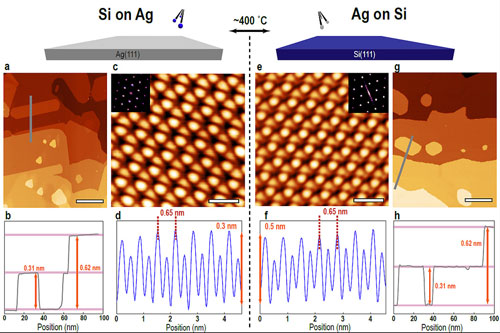
His work focuses on silicene, a recent and exciting addition to the class of two-dimensional materials. Silicene is made up of an almost flat hexagonal pattern of silicon atoms. Every second atom in each hexagonal ring is slightly lifted, resulting in a buckled sheet that looks the same from the top or the bottom.

A Sept. 9, 2014 Canadian Light Source news release, which originated the news item, provides background as to how Johnson started studying silicene and some details about the work,

In 2012, mere months before Johnson began to study silicene, it was discovered and first created by the research group of Prof. Guy Le Lay of Aix-Marseille University, using silver as a base for the thin film. The Le Lay group is the world-leader in silicene growth, and taught Johnson and his colleagues how to make it at the CLS themselves.

“I read the paper when the Le Lay announced they had made silicene, and within three or four months, Alex had arranged for us to travel down to the Advanced Light Source with these people who had made it for the first time,” says Johnson. It was an exciting collaboration for the young physicist.

“This paper had already been cited over a hundred times in a matter of months. It was a major paper, and we were going to measure this new material that no one had really started doing experiments on yet.”

The most pressing question facing silicene research was its potential as a semiconductor. Today, most electronics use silicon as a switch, and researchers looking for new materials to manage quantum effects in computing could easily use the 2-D version if it was also semiconducting.

Calculations had shown that because of the special buckling of silicene, it would have what’s called a Dirac cone – a special electronic structure that could allow researchers to tune the band gap, or the energy space between electron levels. The band gap is what makes a semiconductor: if the space is too small, the material is simply a conductor. Too large, and there is no conduction at all.

Since silicene has only ever been made on a silver base, the materials community also wondered if silicene would maintain its semiconducting properties in this condition. Though its atomic structure is slightly different than freestanding silicene, it was still predicted to have a band gap. However, silver is a metal, which may make the silicene act as a metal as well.

No one really knew how silicene would behave on its silver base.

To adapt the Le Lay group’s silicene-growing process to the equipment at the CLS took several days of work. Though their team had succeeded in silicene synthesis at the Advanced Light Source at Berkeley lab, they had no way to keep those samples under vacuum to prevent them from oxygen damage. Thanks to the work of fellow beamteam members Drs. David Muir and Israel Perez, samples grown at the CLS could be produced, transported and measured in a matter of hours without ever leaving a vacuum chamber.

Johnson grew the silicene sheets at the Resonant Elastic and Inelastic X-ray Scattering (REIXS), beamline, then transferred them in a vacuum to the XAS/XES endstation for analysis. Finally, Johnson could find the answer to the silicene question.

“I didn’t really know what to expect until I saw the XAS and XES on the same energy scale, and I thought to myself, that looks like a metal,” says Johnson.

And while that result is unfortunate for those searching for a new computing wonder material, it does provide some vital information to that search.

“Our result does help to guide the hunt for 2-D silicon in the future, suggesting that metallic substrates should be avoided at all costs,” Johnson explains. “We’re hopeful that we can grow a similar structure on other substrates, ideally ones that leave the semiconducting nature of silicene intact.”

That work is already in process, with Johnson and his colleagues planning to explore three other growing bases this summer, along with multilayers and nanoribbons of silicene.

Like the Dutch researchers in the Jan. 12, 2014 posting, Johnson finds that silicene is not serious competition for graphene (as regards to its electrical properties), but he does not challenge its existence. He does note problems with the silver substrate although he comes to a different conclusion than did the Argonne National Laboratory researchers (Aug. 1,  2014 posting).

Here’s a link to and a citation for Johnson’s paper,

The Metallic Nature of Epitaxial Silicene Monolayers on Ag(111) by Neil W. Johnson, Patrick Vogt, Andrea Resta, Paola De Padova, Israel Perez, David Muir, Ernst Z. Kurmaev, Guy Le Lay, and Alexander Moewes. Advanced Functional Materials Volume 24, Issue 33, pages 5253–5259, September 3, 2014 DOI: 10.1002/adfm.201400769 Article first published online: 10 JUN 2014

This paper is behind a paywall.

A query into the existence of silicene

There’s some fascinating work on silicene at the Argonne National Laboratory which questions current scientific belief as per a July 25, 2014 news item on Nanowerk (Note: A link has been removed),

Sometimes, scientific findings can shake the foundations of what was once held to be true, causing us to step back and re-examine our basic assumptions.

A recent study (“Silicon Growth at the Two-Dimensional Limit on Ag(111)”) at the U.S. Department of Energy’s Argonne National Laboratory has called into question the existence of silicene, thought to be one of the world’s newest and hottest two-dimensional nanomaterials. The study may have great implications to a multi-billion dollar electronics industry that seeks to revolutionize technology at scales 80,000 times smaller than the human hair.

A July 24, 2014 Argonne National Laboratory news release by Justin H.S. Breaux , which originated the news item, describes both silicene and silicon in preparation for the discussion about whether or not silicene exists,

Silicene was proposed as a two-dimensional sheet of silicon atoms that can be created experimentally by super-heating silicon and evaporating atoms onto a silver platform. Silver is the platform of choice because it will not affect the silicon via chemical bonding nor should alloying occur due to its low solubility. During the heating process, as the silicon atoms fall onto the platform, researchers believed that they were arranging themselves in certain ways to create a single sheet of interlocking atoms.

Silicon, on the other hand, exists in three dimensions and is one of the most common elements on Earth. A metal, semiconductor and insulator, purified silicon is extremely stable and has become essential to the integrated circuits and transistors that run most of our computers.

Both silicene and silicon should react immediately with oxygen, but they react slightly differently. In the case of silicon, oxygen breaks some of the silicon bonds of the first one or two atomic layers to form a layer of silicon-oxygen. This, surprisingly, acts a chemical barrier to prevent the decay of the lower layers.

Because it consists of only one layer of silicon atoms, silicene must be handled in a vacuum. Exposure to any amount of oxygen would completely destroy the sample.

This difference is one of the keys to the researchers’ discovery. After depositing the atoms onto the silver platform, initial tests identified that alloy-like surface phases would form until bulk silicon layers, or “platelets” would precipitate out, which has been mistaken as two-dimensional silicene.

The news release next describes how the scientists solved the puzzle,

“Some of the bulk silicon platelets were more than one layer thick,” said Argonne scientist Nathan Guisinger of Argonne’s Center for Nanoscale Materials. “We determined that if we were dealing with multiple layers of silicon atoms, we could bring it out of our ultra-high vacuum chamber and bring it into air and do some other tests.”

“Everybody assumed the sample would immediately decay as soon as they pulled it out of the chamber,” added Northwestern University graduate student Brian Kiraly, one of the principal authors of the study. “We were the first to actually bring it out and perform major experiments outside of the vacuum.”

Each new series of experiments presented a new set of clues that this was, in fact, not silicene.

By examining and categorizing the top layers of the material, the researchers discovered silicon oxide, a sign of oxidation in the top layers. They were also surprised to find that particles from the silver platform alloyed with the silicon at significant depths.

“We found out that what previous researchers identified as silicene is really just a combination of the silicon and the silver,” said Northwestern graduate student Andrew Mannix.

For their final test, the researchers decided to probe the atomic signature of the material.

Materials are made up of systems of atoms that bond and vibrate in unique ways. Raman spectroscopy allows researchers to measure these bonds and vibrations. Housed within the Center for Nanoscale Materials, a DOE Office of Science User Facility, the spectroscope allows researchers to use light to “shift” the position of one atom in a crystal lattice, which in turn causes a shift in the position of its neighbors. Scientists define a material by measuring how strong or weak these bonds are in relation to the frequency at which the atoms vibrate.

The researchers noticed something oddly familiar when looking at the vibrational signatures and frequencies of their sample. Their sample did not exhibit characteristic vibrations of silicene, but it did match those of silicon.

“Having this many research groups and papers potentially be wrong does not happen often,” says Guisinger. “I hope our research helps guide future studies and convincingly demonstrates that silver is not a good platform if you are trying to grow silicene.”

Here’s an image illustrating the vibrational signatures of what scientists had believed to be silicene,

Argonne researchers investigating the properties of silicene (a one-atom thick sheet of silicon atoms) compared scanning tunneling microscope images of atomic silicon growth on silver and atomic silver growth on silicon. The study finds that both growth processes exhibit identical heights and shapes (a, g), indistinguishable honeycomb structures (c, e) and atomic periodicity (d, f). This suggests the growth of bulk silicon on silver, with a silver-induced surface reconstruction, rather than silicene. Courtesy: Argonne National Laboratory

Argonne researchers investigating the properties of silicene (a one-atom thick sheet of silicon atoms) compared scanning tunneling microscope images of atomic silicon growth on silver and atomic silver growth on silicon. The study finds that both growth processes exhibit identical heights and shapes (a, g), indistinguishable honeycomb structures (c, e) and atomic periodicity (d, f). This suggests the growth of bulk silicon on silver, with a silver-induced surface reconstruction, rather than silicene. Courtesy: Argonne National Laboratory

Here’s a link to and a citation for the paper,

Silicon Growth at the Two-Dimensional Limit on Ag(111) by Andrew J. Mannix, Brian Kiraly, Brandon L. Fisher, Mark C. Hersam, and Nathan P. Guisinger. ACS Nano, 2014, 8 (7), pp 7538–7547 DOI: 10.1021/nn503000w Publication Date (Web): July 5, 2014

Copyright © 2014 American Chemical Society

This paper is behind a paywall.

It will be interesting to note what kind of a response the Argonne researchers receive from the scientific community. As for ‘silicene’ items on this blog, there’s a Jan. 14, 2014 posting about work on silicene at the University of Twente (Netherlands). That research was instrumental in helping a student achieve a master’s degree.  While I can describe the Argonne research as fascinating, I imagine the student who got a master’s degree has a different adjective.

Suicide at the nanoscale: the truth about silicene

Researchers at the University of Twente (Netherlands) have shown that silicene, a material of great interest to the semi-conductor industry, has a serious drawback according to a Jan. 14, 2014 news item on Nanowerk,

The semiconductor industry of the future had high expectations of the new material silicene, which shares a lot of similarities with the ‘wonder material’ graphene. However, researchers of the MESA+ Research Institute of the University of Twente – who recently managed to directly and in real time film the formation of silicene – are harshly bursting the bubble: their research shows that silicene has suicidal tendencies.

The Jan. 8, 2014 University of Twente news release, which originated the news item, describes the problem in detail starting with an explanation of silicene,

The material silicene was first created in 2010. Just like graphene, it consists of a single layer of atoms arranged in a honeycomb pattern. Graphene consists of carbon atoms, silicene of silicon atoms.

Because of their special properties – both materials are very strong, thin and flexible and have good electrical conductivity – graphene and silicene seem very well suited for the semiconductor industry of the future. After all, the parts on computer chips have to become smaller and smaller and the limits of the miniaturization of parts made of silicon are drawing closer and closer. The material silicene seems to be several steps ahead of graphene, because the semiconductor industry has been using silicon (which, like silicene, consists of silicon atoms) for many years now. In addition, it is easier to realize a so-called bandgap in silicene, which is a prerequisite for a transistor.

Researchers of the MESA+ Research Institute of the University of Twente have, for the first time, managed to directly and in real time capture the formation of silicene on film. They let evaporated silicon atoms precipitate on a surface of silver, so that a nice, almost closed, singular layer of silicene was formed.

So far so good, but the moment that a certain amount of silicon atoms fall on top of the formed silicene layer, a silicon crystal (silicon in a diamond crystal structure instead of in a honeycomb structure) is formed, which triggers the further crystallization of the material; an irreversible process. From that moment, the newly formed silicon eats the silicene, so to speak.

The reason for this is that the regular crystal structure (diamond) of silicon is energetically more favourable than the honeycomb structure of silicene and therefore more stable. Because of this property, the researchers did not succeed in covering more than 97 per cent of the silver surface with silicene, nor were they able to create multi-layered silicene. In other words: the moment a surface is almost completely covered with silicene, the material commits suicide and simple silicon is formed. The researchers do not expect it to be possible to create multi-layered silicene on a different type of surface, because the influence of the surface on the formation of the second layer of silicene is negligible.

The researchers have produced a video demonstrating their findings,

SiliceneDeposition from University of Twente on Vimeo.

 Caption: Formation of silicene on a silver surface (grey, start of the film). On top of the silver, silicene islands gradually start to form (black, halfway through the film). When the surface is almost completely covered, these collapse into silicon crystals again (black dots in grey areas, end of the film).

The news release ends on a personal note,

The research has been conducted by Adil Acun, Bene Poelsema, Harold Zandvliet and Raoul van Gastel of the department of Physics of Interfaces and Nanomaterials (PIN) of the University of Twente’s MESA+ Research Institute. The research has been published by the renowned academic journal Applied Physics Letters.  What’s even more special about this publication is that it has resulted from the final thesis research of Adil Acun, who was following the master’s programme Applied Physics at the time. He is now working as a PhD candidate at the PIN department.

Here’s link to and a citation for the paper,

The instability of silicene on Ag(111) by A. Acun, B. Poelsema, H. J. W. Zandvliet, and R. van Gastel.  Appl. Phys. Lett. 103, 263119 (2013); http://dx.doi.org/10.1063/1.4860964

This paper is open access as of Jan. 14, 2014.