Tag Archives: silver nanowires

A tangle of silver nanowires for brain-like action

I’ve been meaning to get to this news item from late 2019 as it features work from a team that I’ve been following for a number of years now. First mentioned here in an October 17, 2011 posting, James Gimzewski has been working with researchers at the University of California at Los Angeles (UCLA) and researchers at Japan’s National Institute for Materials Science (NIMS) on neuromorphic computing.

This particular research had a protracted rollout with the paper being published in October 2019 and the last news item about it being published in mid-December 2019.

A December 17, 2029 news item on Nanowerk was the first to alert me to this new work (Note: A link has been removed),

UCLA scientists James Gimzewski and Adam Stieg are part of an international research team that has taken a significant stride toward the goal of creating thinking machines.

Led by researchers at Japan’s National Institute for Materials Science, the team created an experimental device that exhibited characteristics analogous to certain behaviors of the brain — learning, memorization, forgetting, wakefulness and sleep. The paper, published in Scientific Reports (“Emergent dynamics of neuromorphic nanowire networks”), describes a network in a state of continuous flux.

A December 16, 2019 UCLA news release, which originated the news item, offers more detail (Note: A link has been removed),

“This is a system between order and chaos, on the edge of chaos,” said Gimzewski, a UCLA distinguished professor of chemistry and biochemistry, a member of the California NanoSystems Institute at UCLA and a co-author of the study. “The way that the device constantly evolves and shifts mimics the human brain. It can come up with different types of behavior patterns that don’t repeat themselves.”

The research is one early step along a path that could eventually lead to computers that physically and functionally resemble the brain — machines that may be capable of solving problems that contemporary computers struggle with, and that may require much less power than today’s computers do.

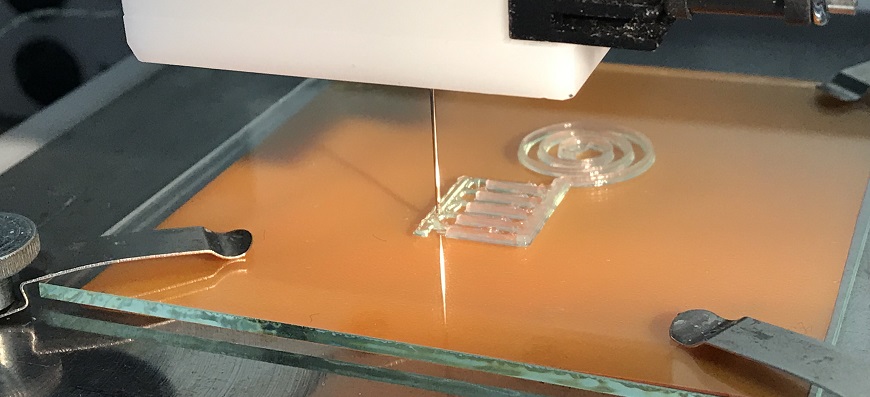
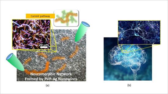
The device the researchers studied is made of a tangle of silver nanowires — with an average diameter of just 360 nanometers. (A nanometer is one-billionth of a meter.) The nanowires were coated in an insulating polymer about 1 nanometer thick. Overall, the device itself measured about 10 square millimeters — so small that it would take 25 of them to cover a dime.

Allowed to randomly self-assemble on a silicon wafer, the nanowires formed highly interconnected structures that are remarkably similar to those that form the neocortex, the part of the brain involved with higher functions such as language, perception and cognition.

One trait that differentiates the nanowire network from conventional electronic circuits is that electrons flowing through them cause the physical configuration of the network to change. In the study, electrical current caused silver atoms to migrate from within the polymer coating and form connections where two nanowires overlap. The system had about 10 million of these junctions, which are analogous to the synapses where brain cells connect and communicate.

The researchers attached two electrodes to the brain-like mesh to profile how the network performed. They observed “emergent behavior,” meaning that the network displayed characteristics as a whole that could not be attributed to the individual parts that make it up. This is another trait that makes the network resemble the brain and sets it apart from conventional computers.

After current flowed through the network, the connections between nanowires persisted for as much as one minute in some cases, which resembled the process of learning and memorization in the brain. Other times, the connections shut down abruptly after the charge ended, mimicking the brain’s process of forgetting.

In other experiments, the research team found that with less power flowing in, the device exhibited behavior that corresponds to what neuroscientists see when they use functional MRI scanning to take images of the brain of a sleeping person. With more power, the nanowire network’s behavior corresponded to that of the wakeful brain.

The paper is the latest in a series of publications examining nanowire networks as a brain-inspired system, an area of research that Gimzewski helped pioneer along with Stieg, a UCLA research scientist and an associate director of CNSI.

“Our approach may be useful for generating new types of hardware that are both energy-efficient and capable of processing complex datasets that challenge the limits of modern computers,” said Stieg, a co-author of the study.

The borderline-chaotic activity of the nanowire network resembles not only signaling within the brain but also other natural systems such as weather patterns. That could mean that, with further development, future versions of the device could help model such complex systems.

In other experiments, Gimzewski and Stieg already have coaxed a silver nanowire device to successfully predict statistical trends in Los Angeles traffic patterns based on previous years’ traffic data.

Because of their similarities to the inner workings of the brain, future devices based on nanowire technology could also demonstrate energy efficiency like the brain’s own processing. The human brain operates on power roughly equivalent to what’s used by a 20-watt incandescent bulb. By contrast, computer servers where work-intensive tasks take place — from training for machine learning to executing internet searches — can use the equivalent of many households’ worth of energy, with the attendant carbon footprint.

“In our studies, we have a broader mission than just reprogramming existing computers,” Gimzewski said. “Our vision is a system that will eventually be able to handle tasks that are closer to the way the human being operates.”

The study’s first author, Adrian Diaz-Alvarez, is from the International Center for Material Nanoarchitectonics at Japan’s National Institute for Materials Science. Co-authors include Tomonobu Nakayama and Rintaro Higuchi, also of NIMS; and Zdenka Kuncic at the University of Sydney in Australia.

Caption: (a) Micrograph of the neuromorphic network fabricated by this research team. The network contains of numerous junctions between nanowires, which operate as synaptic elements. When voltage is applied to the network (between the green probes), current pathways (orange) are formed in the network. (b) A Human brain and one of its neuronal networks. The brain is known to have a complex network structure and to operate by means of electrical signal propagation across the network. Credit: NIMS

A November 11, 2019 National Institute for Materials Science (Japan) press release (also on EurekAlert but dated December 25, 2019) first announced the news,

An international joint research team led by NIMS succeeded in fabricating a neuromorphic network composed of numerous metallic nanowires. Using this network, the team was able to generate electrical characteristics similar to those associated with higher order brain functions unique to humans, such as memorization, learning, forgetting, becoming alert and returning to calm. The team then clarified the mechanisms that induced these electrical characteristics.

The development of artificial intelligence (AI) techniques has been rapidly advancing in recent years and has begun impacting our lives in various ways. Although AI processes information in a manner similar to the human brain, the mechanisms by which human brains operate are still largely unknown. Fundamental brain components, such as neurons and the junctions between them (synapses), have been studied in detail. However, many questions concerning the brain as a collective whole need to be answered. For example, we still do not fully understand how the brain performs such functions as memorization, learning and forgetting, and how the brain becomes alert and returns to calm. In addition, live brains are difficult to manipulate in experimental research. For these reasons, the brain remains a “mysterious organ.” A different approach to brain research?in which materials and systems capable of performing brain-like functions are created and their mechanisms are investigated?may be effective in identifying new applications of brain-like information processing and advancing brain science.

The joint research team recently built a complex brain-like network by integrating numerous silver (Ag) nanowires coated with a polymer (PVP) insulating layer approximately 1 nanometer in thickness. A junction between two nanowires forms a variable resistive element (i.e., a synaptic element) that behaves like a neuronal synapse. This nanowire network, which contains a large number of intricately interacting synaptic elements, forms a “neuromorphic network”. When a voltage was applied to the neuromorphic network, it appeared to “struggle” to find optimal current pathways (i.e., the most electrically efficient pathways). The research team measured the processes of current pathway formation, retention and deactivation while electric current was flowing through the network and found that these processes always fluctuate as they progress, similar to the human brain’s memorization, learning, and forgetting processes. The observed temporal fluctuations also resemble the processes by which the brain becomes alert or returns to calm. Brain-like functions simulated by the neuromorphic network were found to occur as the huge number of synaptic elements in the network collectively work to optimize current transport, in the other words, as a result of self-organized and emerging dynamic processes..

The research team is currently developing a brain-like memory device using the neuromorphic network material. The team intends to design the memory device to operate using fundamentally different principles than those used in current computers. For example, while computers are currently designed to spend as much time and electricity as necessary in pursuit of absolutely optimum solutions, the new memory device is intended to make a quick decision within particular limits even though the solution generated may not be absolutely optimum. The team also hopes that this research will facilitate understanding of the brain’s information processing mechanisms.

This project was carried out by an international joint research team led by Tomonobu Nakayama (Deputy Director, International Center for Materials Nanoarchitectonics (WPI-MANA), NIMS), Adrian Diaz Alvarez (Postdoctoral Researcher, WPI-MANA, NIMS), Zdenka Kuncic (Professor, School of Physics, University of Sydney, Australia) and James K. Gimzewski (Professor, California NanoSystems Institute, University of California Los Angeles, USA).

Here at last is a link to and a citation for the paper,

Emergent dynamics of neuromorphic nanowire networks by Adrian Diaz-Alvarez, Rintaro Higuchi, Paula Sanz-Leon, Ido Marcus, Yoshitaka Shingaya, Adam Z. Stieg, James K. Gimzewski, Zdenka Kuncic & Tomonobu Nakayama. Scientific Reports volume 9, Article number: 14920 (2019) DOI: https://doi.org/10.1038/s41598-019-51330-6 Published: 17 October 2019

This paper is open access.

Nanocellulose sensors: 3D printed and biocompatible

I do like to keep up with nanocellulose doings, especially when there’s some Canadian involvement, and an October 8, 2019 news item on Nanowerk alerted me to a newish application for the product,

Physiological parameters in our blood can be determined without painful punctures. Empa researchers are currently working with a Canadian team to develop flexible, biocompatible nanocellulose sensors that can be attached to the skin. The 3D-printed analytic chips made of renewable raw materials will even be biodegradable in future.

The idea of measuring parameters that are relevant for our health via the skin has already taken hold in medical diagnostics. Diabetics, for example, can painlessly determine their blood sugar level with a sensor instead of having to prick their fingers.

An October 8, 2019 Empa (Swiss Federal Laboratories for Materials Science and Technology) press release, which originated the news item, provides more detail,

A transparent foil made of wood

Nanocellulose is an inexpensive, renewable raw material, which can be obtained in form of crystals and fibers, for example from wood. However, the original appearance of a tree no longer has anything to do with the gelatinous substance, which can consist of cellulose nanocrystals and cellulose nanofibers. Other sources of the material are bacteria, algae or residues from agricultural production. Thus, nanocellulose is not only relatively easy and sustainable to obtain. Its mechanical properties also make the “super pudding” an interesting product. For instance, new composite materials based on nanocellulose can be developed that could be used as surface coatings, transparent packaging films or even to produce everyday objects like beverage bottles.

Researchers at Empa’s Cellulose & Wood Materials lab and Woo Soo Kim from the Simon Fraser University [SFU] in Burnaby, Canada, are also focusing on another feature of nanocellulose: biocompatibility. Since the material is obtained from natural resources, it is particularly suitable for biomedical research.

With the aim of producing biocompatible sensors that can measure important metabolic values, the researchers used nanocellulose as an “ink” in 3D printing processes. To make the sensors electrically conductive, the ink was mixed with silver nanowires. The researchers determined the exact ratio of nanocellulose and silver threads so that a three-dimensional network could form.

Just like spaghetti – only a wee bit smaller

It turned out that cellulose nanofibers are better suited than cellulose nanocrystals to produce a cross-linked matrix with the tiny silver wires. “Cellulose nanofibers are flexible similar to cooked spaghetti, but with a diameter of only about 20 nanometers and a length of just a few micrometers,” explains Empa researcher Gilberto Siqueira.

The team finally succeeded in developing sensors that measure medically relevant metabolic parameters such as the concentration of calcium, potassium and ammonium ions. The electrochemical skin sensor sends its results wirelessly to a computer for further data processing. The tiny biochemistry lab on the skin is only half a millimeter thin.

While the tiny biochemistry lab on the skin – which is only half a millimeter thin – is capable of determining ion concentrations specifically and reliably, the researchers are already working on an updated version. “In the future, we want to replace the silver [nano] particles with another conductive material, for example on the basis of carbon compounds,” Siqueira explains. This would make the medical nanocellulose sensor not only biocompatible, but also completely biodegradable.

I like the images from Empa better than the ones from SFU,

Using a 3D printer, the nanocellulose “ink” is applied to a carrier plate. Silver particles provide the electrical conductivity of the material. Image: Empa
Empa researcher Gilberto Siqueira demonstrates the newly printed nanocellulose circuit. After a subsequent drying, the material can be further processed. Image: Empa

SFU produced a news release about this work back in February 2019. Again, I prefer what the Swiss have done because they’re explaining/communicating the science, as well as , communicating benefits. From a February 13, 2019 SFU news release (Note: Links have been removed),

Simon Fraser University and Swiss researchers are developing an eco-friendly, 3D printable solution for producing wireless Internet-of-Things (IoT) sensors that can be used and disposed of without contaminating the environment. Their research has been published as the cover story in the February issue of the journal Advanced Electronic Materials.

SFU professor Woo Soo Kim is leading the research team’s discovery, which uses a wood-derived cellulose material to replace the plastics and polymeric materials currently used in electronics.

Additionally, 3D printing can give flexibility to add or embed functions onto 3D shapes or textiles, creating greater functionality.

“Our eco-friendly, 3D-printed cellulose sensors can wirelessly transmit data during their life, and then can be disposed without concern of environmental contamination,” says Kim, a professor in the School of Mechatronic Systems Engineering. The SFU research is being carried out at PowerTech Labs in Surrey, which houses several state-of-the-art 3D printers used to advance the research.

“This development will help to advance green electronics. For example, the waste from printed circuit boards is a hazardous source of contamination to the environment. If we are able to change the plastics in PCB to cellulose composite materials, recycling of metal components on the board could be collected in a much easier way.”

Kim’s research program spans two international collaborative projects, including the latest focusing on the eco-friendly cellulose material-based chemical sensors with collaborators from the Swiss Federal Laboratories for Materials Science.

He is also collaborating with a team of South Korean researchers from the Daegu Gyeongbuk Institute of Science and Technology’s (DGIST)’s department of Robotics Engineering, and PROTEM Co Inc, a technology-based company, for the development of printable conductive ink materials.

In this second project, researchers have developed a new breakthrough in the embossing process technology, one that can freely imprint fine circuit patterns on flexible polymer substrate, a necessary component of electronic products.

Embossing technology is applied for the mass imprinting of precise patterns at a low unit cost. However, Kim says it can only imprint circuit patterns that are imprinted beforehand on the pattern stamp, and the entire, costly stamp must be changed to put in different patterns.

The team succeeded in developing a precise location control system that can imprint patterns directly resulting in a new process technology. The result will have widespread implications for use in semiconductor processes, wearable devices and the display industry.

This paper was made available online back in December 2018 and then published in print in February 2019. As to why there’d be such large gaps between the paper’s publication dates and the two institution’s news/press releases, it’s a mystery to me. In any event, here’s a link to and a citation for the paper,

3D Printed Disposable Wireless Ion Sensors with Biocompatible Cellulose Composites by Taeil Kim, Chao Bao, Michael Hausmann, Gilberto Siqueira, Tanja Zimmermann, Woo Soo Kim. Advanced Electronic Materials DOI: https://doi.org/10.1002/aelm.201970007 First published online December 19, 2018. First published in print: 08 February 2019 (Adv. Electron. Mater. 2/2109) Volume 5, Issue 2 February 2019 1970007

This paper is behind a paywall.

Replacing the indium tin oxide (ITO) electrodes in smartphones?

Physicists have developed silver nanowires that could be used to replace the indium tin oxide electrodes found in touchscreens for smartphones, tablets, and more. From a Sept. 14, 2016 news item on Nanowerk,

Physicists at the University of Sussex are at an advanced stage of developing alternative touchscreen technology to overcome the shortfall in the traditional display, phone and tablet material that relies on electrodes made from indium tin oxide (ITO).

They have now shown that not only is the material suitable for touchscreens, but that it is possible to produce extremely small patterns (pixels), small enough for high definition LCD displays, such as smartphones and the next generation of television and computer screens.

The study, led by Sussex Professor of Experimental Physics Alan Dalton, investigates some of the intricacies of patterning silver nanowire films to produce detailed electrode structures. …

A Sept. 13, 2016 University of Sussex press release, which originated the news item, describes why this research presents some exciting possibilities (Note: Links have been removed),

Previous research by Professor Dalton’s group has shown that silver nanowires not only match the transmittances and conductivities of ITO films but exceed them. This makes the material very attractive for touch screens. However, the group have now shown, for the first time, that this type of nanomaterial is compatible with more demanding applications such as LCD and OLED displays.

Professor Dalton said: “Display technologies such as LCD and OLED form images using pixels. Each pixel of these displays is further broken down into subpixels; typically, one each for red, green and blue colours. In the display in a smartphone, for example, these subpixels are less than a sixth of the width of a human hair – which is also similar in length to the silver nanowires used in our research.”

Dr Matthew Large, the lead author of the paper, expanded: “In this research we have applied a mathematical technique to work out the smallest subpixel size we can make without affecting the properties of our nanowire electrodes. This method was originally developed to describe how phase changes like freezing happen in very small spaces, The results tell us how to tune our nanowires to meet the requirements of any given application.”

In collaboration with their industrial partners, M-SOLV based in Oxford, the team – which is now looking to apply these research results to commercial projects – has also demonstrated that the incorporation of silver nanowires into a multi-touch sensor actually reduces the production cost and energy usage.

Professor Dalton said: “Silver nanowire and silver nanowire/graphene hybrids are probably the most viable alternatives to existing technologies. Others scientists have studied several alternative materials, but the main issue is that the majority of other materials do not effectively compete with ITO or they are too costly to produce, at least at the moment.”

Here’s a link to and a citation for the paper,

Finite-size scaling in silver nanowire films: design considerations for practical devices by Matthew J. Large, Maria Cann, Sean P. Ogilvie, Alice A. K. King, Izabela Jurewicz, and Alan B. Dalton. Nanoscale, (issue 28) 2016,8, 13701-13707 DOI: 10.1039/C6NR03960J First published online 27 Jun 2016

This paper is behind a paywall.

Dexter Johnson’s Sept. 16, 2016 posting (on his Nanoclast blog on the IEEE [Institute of Electrical and Electronics Engineers] website) adds some new detail (Note: Links have been removed),

The field of nanomaterials vying to replace indium tin oxide (ITO) as the transparent conductor that controls display pixels in touch screen displays is getting crowded. We’ve seen materials including carbon nanotubes, silver nanowires, and graphene promoted as the heir apparent for this application.

Now, researchers at the University of Sussex in England have introduced a strong contender into the battle to replace indium tin oxide: a hybrid material consisting of silver nanowires that are linked together with graphene.

“The hybrid material is a lot cheaper due to the fact that we only need to use a fraction of the nanowires normally required to attain the properties of ITO,” …

Tune your windows for privacy

Caption: With an applied voltage, the nanowires on either side of the glass become attracted to each other and move toward each other, squeezing and deforming the soft elastomer. Because the nanowires are scattered unevenly across the surface, the elastomer deforms unevenly. That uneven roughness causes light to scatter, turning the glass opaque. Credit: David Clarke/Harvard SEAS [School of Engineering and Applied Sciences]

Right now, this is my favourite science illustration. A March 14, 2016 news item on Nanowerk announces Harvard’s new technology that can turn a clear window into an opaque one at the touch of a switch,

Say goodbye to blinds.

Researchers at the Harvard John A. Paulson School of Engineering and Applied Sciences have developed a technique that can quickly change the opacity of a window, turning it cloudy, clear or somewhere in between with the flick of a switch.

Tunable windows aren’t new but most previous technologies have relied on electrochemical reactions achieved through expensive manufacturing. This technology, developed by David Clarke, the Extended Tarr Family Professor of Materials, and postdoctoral fellow Samuel Shian, uses geometry [to] adjust the transparency of a window.

A March 14, 2016 Harvard University news release (also on EurekAlert) by Leah Burrows, which originated the news item, describes the technology in more detail,

The tunable window is comprised of a sheet of glass or plastic, sandwiched between transparent, soft elastomers sprayed with a coating of silver nanowires, too small to scatter light on their own.

But apply an electric voltage and things change quickly.

With an applied voltage, the nanowires on either side of the glass are energized to move toward each other, squeezing and deforming the soft elastomer. Because the nanowires are distributed unevenly across the surface, the elastomer deforms unevenly. The resulting uneven roughness causes light to scatter, turning the glass opaque.

The change happens in less than a second.

It’s like a frozen pond, said Shian.

“If the frozen pond is smooth, you can see through the ice. But if the ice is heavily scratched, you can’t see through,” said Shian.

Clarke and Shian found that the roughness of the elastomer surface depended on the voltage, so if you wanted a window that is only light clouded, you would apply less voltage than if you wanted a totally opaque window.

“Because this is a physical phenomenon rather than based on a chemical reaction, it is a simpler and potentially cheaper way to achieve commercial tunable windows,” said Clarke.

Current chemical-based controllable windows use vacuum deposition to coat the glass, a process that deposits layers of a material molecule by molecule. It’s expensive and painstaking. In Clarke and Shian’s method, the nanowire layer can be sprayed or peeled onto the elastomer, making the technology scalable for larger architectural projects.

Next the team is working on incorporating thinner elastomers, which would require lower voltages, more suited for standard electronical supplies.

Here’s a link to and a citation for the paper,

Electrically tunable window device by Samuel Shian and David R. Clarke. Optics Letters Vol. 41, Issue 6, pp. 1289-1292 (2016) •doi: 10.1364/OL.41.001289

This is an open access paper.

Saving silver; a new kind of electrode

An Aug. 1, 2015 news item on Nanotechnology Now highlights work from Germany’s Helmholtz-Zentrum Berlin für Materialien und Energie (Helmholtz Zentrum Berlin),

The electrodes for connections on the “sunny side” of a solar cell need to be not just electrically conductive, but transparent as well. As a result, electrodes are currently made either by using thin strips of silver in the form of a coarse-meshed grid squeegeed onto a surface, or by applying a transparent layer of electrically conductive indium tin oxide (ITO) compound. Neither of these are ideal solutions, however. This is because silver is a precious metal and relatively expensive, and silver particles with nanoscale dimensions oxidise particularly rapidly; meanwhile, indium is one of the rarest elements on earth crust and probably will only continue to be available for a few more years.

Manuela Göbelt on the team of Prof. Silke Christiansen has now developed an elegant new solution using only a fraction of the silver and entirely devoid of indium to produce a technologically intriguing electrode. The doctoral student initially made a suspension of silver nanowires in ethanol using wet-chemistry techniques. She then transferred this suspension with a pipette onto a substrate, in this case a silicon solar cell. As the solvent is evaporated, the silver nanowires organise themselves into a loose mesh that remains transparent, yet dense enough to form uninterrupted current paths.

A July 31, 2015 Helmholtz Zentrum Berlin press release (also on EurekAlert), which originated the news item, describes the work in more detail,

Subsequently, Göbelt used an atomic layer deposition technique to gradually apply a coating of a highly doped wide bandgap semiconductor known as AZO. AZO consists of zinc oxide that is doped with aluminium. It is much less expensive than ITO and just as transparent, but not quite as electrically conductive. This process caused tiny AZO crystals to form on the silver nanowires, enveloped them completely, and finally filled in the interstices. The silver nanowires, measuring about 120 nanometres in diameter, were covered with a layer of about 100 nanometres of AZO and encapsulated by this process.

Quality map calculated

Measurements of the electrical conductivity showed that the newly developed composite electrode is comparable to a conventional silver grid electrode. However, its performance depends on how well the nanowires are interconnected, which is a function of the wire lengths and the concentration of silver nanowires in the suspension. The scientists were able to specify the degree of networking in advance with computers. Using specially developed image analysis algorithms, they could evaluate images taken with a scanning electron microscope and predict the electrical conductivity of the electrodes from them.

“We are investigating where a given continuous conductive path of nanowires is interrupted to see where the network is not yet optimum”, explains Ralf Keding. Even with high-performance computers, it still initially took nearly five days to calculate a good “quality map” of the electrode. The software is now being optimised to reduce the computation time. “The image analysis has given us valuable clues about where we need to concentrate our efforts to increase the performance of the electrode, such as increased networking to improve areas of poor coverage by changing the wire lengths or the wire concentration in solution”, says Göbelt.

Practical aternative to conventional electrodes

“We have developed a practical, cost-effective alternative to conventional screen-printed grid electrodes and to the common ITO type that is threatened however by material bottlenecks”, says Christiansen, who heads the Institute of Nanoarchitectures for Energy Conversion at HZB and additionally directs a project team at the Max Planck Institute for the Science of Light (MPL).

Only a fraction of silver, nearly no shadow effects

The new electrodes can actually be made using only 0.3 grams of silver per square metre, while conventional silver grid electrodes require closer to between 15 and 20 grams of silver. In addition, the new electrode casts a considerably smaller shadow on the solar cell. “The network of silver nanowires is so fine that almost no light for solar energy conversion is lost in the cell due to the shadow”, explains Göbelt. On the contrary, she hopes “it might even be possible for the silver nanowires to scatter light into the solar cell absorbers in a controlled fashion through what are known as plasmonic effects.”

Here’s a link to and a citation for the paper,

Encapsulation of silver nanowire networks by atomic layer deposition for indium-free transparent electrodes by Manuela Göbelt, Ralf Keding, Sebastian W. Schmitt, Björn Hoffmann, Sara Jäckle, Michael Latzel, Vuk V. Radmilović, Velimir R. Radmilović,  Erdmann Spiecker, and Silke Christiansen. Nano Energy Volume 16, September 2015, Pages 196–206 doi:10.1016/j.nanoen.2015.06.027

This paper is behind a paywall.

Hyper stretchable nanogenerator

There’s a lot of talk about flexibility, stretchability and bendability in electronics and the latest is coming from Korea. An April 13, 2015 Korea Advanced Institute for Science and Technology (KAIST) news release on EurekAlert describes the situation and the Korean scientists’ most recent research into stretchable electronics,

A research team led by Professor Keon Jae Lee of the Department of Materials Science and Engineering at the Korea Advanced Institute of Science and Technology (KAIST) has developed a hyper-stretchable elastic-composite energy harvesting device called a nanogenerator.

Flexible electronics have come into the market and are enabling new technologies like flexible displays in mobile phone, wearable electronics, and the Internet of Things (IoTs). However, is the degree of flexibility enough for most applications? For many flexible devices, elasticity is a very important issue. For example, wearable/biomedical devices and electronic skins (e-skins) should stretch to conform to arbitrarily curved surfaces and moving body parts such as joints, diaphragms, and tendons. They must be able to withstand the repeated and prolonged mechanical stresses of stretching. In particular, the development of elastic energy devices is regarded as critical to establish power supplies in stretchable applications. Although several researchers have explored diverse stretchable electronics, due to the absence of the appropriate device structures and correspondingly electrodes, researchers have not developed ultra-stretchable and fully-reversible energy conversion devices properly.

Recently, researchers from KAIST and Seoul National University (SNU) have collaborated and demonstrated a facile methodology to obtain a high-performance and hyper-stretchable elastic-composite generator (SEG) using very long silver nanowire-based stretchable electrodes. Their stretchable piezoelectric generator can harvest mechanical energy to produce high power output (~4 V) with large elasticity (~250%) and excellent durability (over 104 cycles). These noteworthy results were achieved by the non-destructive stress- relaxation ability of the unique electrodes as well as the good piezoelectricity of the device components. The new SEG can be applied to a wide-variety of wearable energy-harvesters to transduce biomechanical-stretching energy from the body (or machines) to electrical energy.

Professor Lee said, “This exciting approach introduces an ultra-stretchable piezoelectric generator. It can open avenues for power supplies in universal wearable and biomedical applications as well as self-powered ultra-stretchable electronics.”

Here’s a link to and a citation for the paper,

A Hyper-Stretchable Elastic-Composite Energy Harvester by Chang Kyu Jeong, Jinhwan Lee, Seungyong Han, Jungho Ryu, Geon-Tae Hwang, Dae Yong Park, Jung Hwan Park, Seung Seob Lee, Mynghwan Byun, Seung Hwan Ko, and Keon Jae Lee. Advanced Materials DOI: 10.1002/adma.201500367 30 March 2015Full

This paper is behind a paywall.

The researchers have prepared a short video (22 secs. and silent),

Silver nanowires have a surprising ability to self-heal

It seems there could be a new member of the flexible electronics materials community, silver nanowires, according to a Jan. 23, 2015 news item on ScienceDaily,

Wth its high electrical conductivity and optical transparency, indium tin oxide is one of the most widely used materials for touchscreens, plasma displays, and flexible electronics. But its rapidly escalating price has forced the electronics industry to search for other alternatives.

One potential and more cost-effective alternative is a film made with silver nanowires–wires so extremely thin that they are one-dimensional–embedded in flexible polymers. Like indium tin oxide, this material is transparent and conductive. But development has stalled because scientists lack a fundamental understanding of its mechanical properties.

A Jan. 23, 2015 Northwestern University news release (also on EurekAlert), which originated the news item, explains what makes silver nanowires a candidate as an alternative to indium tin oxide for use in flexible electronics,

… Horacio Espinosa, the James N. and Nancy J. Farley Professor in Manufacturing and Entrepreneurship at Northwestern University’s McCormick School of Engineering, has led research that expands the understanding of silver nanowires’ behavior in electronics.

Espinosa and his team investigated the material’s cyclic loading, which is an important part of fatigue analysis because it shows how the material reacts to fluctuating loads of stress.

“Cyclic loading is an important material behavior that must be investigated for realizing the potential applications of using silver nanowires in electronics,” Espinosa said. “Knowledge of such behavior allows designers to understand how these conductive films fail and how to improve their durability.”

By varying the tension on silver nanowires thinner than 120 nanometers and monitoring their deformation with electron microscopy, the research team characterized the cyclic mechanical behavior. They found that permanent deformation was partially recoverable in the studied nanowires, meaning that some of the material’s defects actually self-healed and disappeared upon cyclic loading. These results indicate that silver nanowires could potentially withstand strong cyclic loads for long periods of time, which is a key attribute needed for flexible electronics.

“These silver nanowires show mechanical properties that are quite unexpected,” Espinosa said. “We had to develop new experimental techniques to be able to measure this novel material property.”

The findings were recently featured on the cover of the journal Nano Letters. Other Northwestern coauthors on the paper are Rodrigo Bernal, a recently graduated PhD student in Espinosa’s lab, and Jiaxing Huang, associate professor of materials science and engineering in McCormick.

“The next step is to understand how this recovery influences the behavior of these materials when they are flexed millions of times,” said Bernal, first author of the paper.

Here’s a link to and citation for the paper,

Intrinsic Bauschinger Effect and Recoverable Plasticity in Pentatwinned Silver Nanowires Tested in Tension by Rodrigo A. Bernal, Amin Aghaei, Sangjun Lee, Seunghwa Ryu, Kwonnam Sohn, Jiaxing Huang, Wei Cai, and Horacio Espinosa. Nano Lett., 2015, 15 (1), pp 139–146 DOI: 10.1021/nl503237t Publication Date (Web): October 3, 2014
Copyright © 2014 American Chemical Society

This particular version of the paper is behind a paywall. However, access to the paper is possible although I make no claims as to which version it is or whether it will continue to be freely accessible.

LEDs for your contact lenses from Korea’s Ulsan National Institute of Science and Technology

Probably the most exciting application for this work from Korea is where stretchable graphene-metal nanowire electrodes can be fitted to soft contact lenses paving the way for picture-taking and scanning lenses. A May 30, 2013 news item on Nanowerk describes the research in broad terms (Note: A link has been removed),

A hybrid transparent and stretchable electrode could open the new way for flexible displays, solar cells, and even electronic devices fitted on a curvature substrate such as soft eye contact lenses, by the UNIST (Ulsan National Institute of Science and Technology) research team (“High-Performance, Transparent, and Stretchable Electrodes Using Graphene–Metal Nanowire Hybrid Structures”).

The UNIST May 31, 2013 news release by Eunhee Song about the research provides context and detail,

Transparent electrodes are in and of themselves nothing all that new – they have been widely used in things like touch screens, flat-screen TVs, solar cells and light-emitting devices. Currently transparent electrodes are commonly made from a material known as indium tin oxide (ITO). Although it suffices for its job, it’s brittle, cracking and losing functionality if flexed. It also degrades over time, and is somewhat expensive due to the limited quantities of indium metal.

As an alternative, the networks of randomly distributed mNWs [metal nanowires] have been considered as promising candidates for next-generation transparent electrodes, due to their low-cost, high-speed fabrication of transparent electrodes.

However, the number of disadvantage of the mNW networks has limited their integration into commercial devices. They have low breakdown voltage, typically high NW-NW junction resistance, high contact resistance between network and active materials, material instability and poor adhesion to plastic substrates.

UNIST scientists here, combined graphene with silver nanowires to form a thin, transparent and stretchable electrode. Combining graphene and silver nanowires in a hybrid material overcomes weakness of individual material.

Graphene is also well known as good a candidate for transparent electrode because of their unique electrical properties and high mechanical flexibility. However, scalable graphene synthesis methods for commercialization produces lower quality graphene with individual segments called grains which increases the electrical resistance at boundaries between these grains.

Silver nanowires, on the other hand, have high resistance because they are randomly oriented like a jumble of toothpicks facing in different directions. In this random orientation, there are many contact between nanowires, resulting in high resistance due to large junction resistance of nanowires. Due to these drawbacks, neither is good for conducting electricity, but a hybrid structure, combined from two materials, is.

As a result, it presents a high electrical and optical performance with mechanical flexibility and stretchability for flexible electronics. The hybrid Transparent electrode reportedly has a low “sheet resistance” while preserving high transmittance. There’s almost no change in its resistance when bent and folded where ITO is bent, its resistance increases significantly. Additionally the hybrid material reportedly has a low “sheet resistance” while preserving electrical and optical properties reliable against thermal oxidation condition

The graphene-mNW hybrid structure developed by the research team, as a new class of such electrodes, may soon find use in a variety of other applications. The research team demonstrated Inorganic light-emitting diode (ILDED) devices fitted on a soft eye contact lens using the transparent, stretchable interconnects of the hybrid electrodes as an application example.

Here are some images from the research team,

Hybrid transparent and stretchable electrode as part of norganic light-emitting diode (ILDED) devices fitted on a soft eye contact lens. Image courtesy of  Korea's UNIST(Ulsan National Institute of Science and Technology)

Hybrid transparent and stretchable electrode as part of norganic light-emitting diode (ILDED) devices fitted on a soft eye contact lens. Image courtesy of Korea’s UNIST (Ulsan National Institute of Science and Technology)

There has already been an in vivo study of the ‘electrified’ soft contact lens (from the news release),

As an in vivo study, this contact lens was worn by a live rabbit eye for five hours and none of abnormal behavior, such as bloodshot eye or the rubbing of eye areas, of the live rabbit had been observed.

Wearing eye contact lenses, picture-taking and scanning, is not a scene on Sci-Fi movie anymore.

Jang-Ung Park, professor of the School of Nano-Bioscience and Chemical Engineering, UNIST, led the effort.

“We believe the hybridization between two-dimensional and one-dimensional nanomaterials presents a promising strategy toward flexible, wearable electronics and implantable biosensor devices, and indicate the substantial promise of future electronics,” said Prof. Park.

Here’s a close-up of a test bunny’s eye,

Rabbit's (bunny's) eye with Inorganic light-emitting diode (ILDED) devices fitted on a soft eye contact lens (using the transparent, stretchable interconnects of the hybrid electrodes).  Courtesy of UNIST (Ulsan National Institute of Science and Technology)

Rabbit’s (bunny’s) eye with Inorganic light-emitting diode (ILDED) devices fitted on a soft eye contact lens (using the transparent, stretchable interconnects of the hybrid electrodes).
Courtesy of UNIST (Ulsan National Institute of Science and Technology)

I wonder how one would control the picture-taking, scanning capabilities. In any event, here’s a link to and a citation for the research paper,

High-Performance, Transparent, and Stretchable Electrodes Using Graphene–Metal Nanowire Hybrid Structures by Mi-Sun Lee, Kyongsoo Lee, So-Yun Kim, Heejoo Lee, Jihun Park, Kwang-Hyuk Choi, Han-Ki Kim, Dae-Gon Kim, Dae-Young Lee, SungWoo Nam, and Jang-Ung Park. Nano Lett. [Nano Letters], Article ASAP DOI: 10.1021/nl401070p Publication Date (Web): May 23, 2013

Copyright © 2013 American Chemical Society

This paper is behind a paywall.