Tag Archives: solar panels

Plants as a source of usable electricity

A friend sent me a link to this interview with Iftach Yacoby of Tel Aviv University talking about some new research into plants and electricity. From a June 8, 2020 article by Omer Kabir for Calcalist (CTech) on the Algemeiner website,

For years, scientists have been trying to understand the evolutionary capabilities of plants to produce energy and have had only partial success. But a recent Tel Aviv University [TAU] study seems to make the impossible possible, proving that any plant can be transformed into an electrical source, producing a variety of materials that can revolutionize the global economy — from using hydrogen as fuel to clean ammonia to replace the pollutants in the agriculture industry.

“People are unaware that their plant pots have an electric current for everything,” Iftach Yacoby, head of the Laboratory of Renewable Energy Studies at Tel Aviv University’s Faculty of Life Sciences said in a recent interview with Calcalist.

“Our study opens the door to a new field of agriculture, equivalent to wheat or corn production for food security — generating energy,” he said. However, Yacoby makes it clear that it will take at least a decade before the research findings can be transferred to the commercial level.

At the heart of the research is the understanding that plants have particularly efficient capacities when it comes to electricity generation. “Anything green that is not dollars, but rather leaves, grass, and seaweed for example, contains solar panels that are completely identical to the panels the entire country is now building,” Yacoby explained. “They know how to take in solar radiation and make electrons flow out of it. That’s the essence of photosynthesis. Most people think of oxygen and food production, but the most basic phase of photosynthesis is the same as silicon panels in the Negev and on rooftops — taking in sunlight and generating electric current.”

… “At home, an electric current can be wired to many devices. Just plug the device into a power outlet. But when you want to do it in plants, it’s about the order of nanometers. We have no idea where to plug the plugs. That’s what we did in this study. In plant cells, we found they can be used as a socket for anything, at just a nanometer size. We have an enzyme, which is equivalent to a biological machine that can produce hydrogen. We took this enzyme, put it together so that it sits in the socket in the plant cell, which was previously only hypothetical. When he started to produce hydrogen, we proved that we had a socket for everything, though nanotermically-sized. Now we can take any plant or kelp and engineer it so that their electrical outlet can be used for production purposes,” Yacoby explained.

“If you attach an enzyme that produces hydrogen you get hydrogen, it’s the cleanest fuel that can be,” he said. “There are already electric cars and bicycles with a range of 150 km that travel on hydrogen. There are many types of enzymes in nature that produce valuable substances, such as ammonia needed for the fertilizer industry and today is still produced by a very toxic and harmful method that consumes a lot of energy. We can provide a plant-based alternative for the production of materials that are made in chemical manufacturing facilities. It’s an electric platform inside a living plant cell.”

You might find it helpful to read Kabir’s article in its entirety before moving on to the news release about the work. The work was conducted with researchers from Arizona State University (ASU;US) and a researcher from Yogi Vemana University (India), as well as, Yacoby. There’s a May 7, 2020 ASU news release (also on EurekAlert but published on May 6, 2020) detailing the work,

Hydrogen is an essential commodity with over 60 million tons produced globally every year. However over 95 percent of it is made by steam reformation of fossil fuels, a process that is energy intensive and produces carbon dioxide. If we could replace even a part of that with algal biohydrogen that is made via light and water, it would have a substantial impact.

This is essentially what has just been achieved in the lab of Kevin Redding, professor in the School of Molecular Sciences and director of the Center for Bioenergy and Photosynthesis. Their research, entitled Rewiring photosynthesis: a Photosystem I -hydrogenase chimera that makes hydrogen in vivo was published very recently in the high impact journal Energy and Environmental Science.

“What we have done is to show that it is possible to intercept the high energy electrons from photosynthesis and use them to drive alternate chemistry, in a living cell” explained Redding. “We have used hydrogen production here as an example.”

“Kevin Redding and his group have made a true breakthrough in re-engineering the Photosystem I complex,” explained Ian Gould, interim director of the School of Molecular Sciences, which is part of The College of Liberal Arts and Sciences. “They didn’t just find a way to redirect a complex protein structure that nature designed for one purpose to perform a different, but equally critical process, but they found the best way to do it at the molecular level.”

It is common knowledge that plants and algae, as well as cyanobacteria, use photosynthesis to produce oxygen and “fuels,” the latter being oxidizable substances like carbohydrates and hydrogen. There are two pigment-protein complexes that orchestrate the primary reactions of light in oxygenic photosynthesis: Photosystem I (PSI) and Photosystem II (PSII).

Algae (in this work the single-celled green alga Chlamydomonas reinhardtii, or ‘Chlamy’ for short) possess an enzyme called hydrogenase that uses electrons it gets from the protein ferredoxin, which is normally used to ferry electrons from PSI to various destinations. A problem is that the algal hydrogenase is rapidly and irreversibly inactivated by oxygen that is constantly produced by PSII.

In this study, doctoral student and first author Andrey Kanygin has created a genetic chimera of PSI and the hydrogenase such that they co-assemble and are active in vivo. This new assembly redirects electrons away from carbon dioxide fixation to the production of biohydrogen.

“We thought that some radically different approaches needed to be taken — thus, our crazy idea of hooking up the hydrogenase enzyme directly to Photosystem I in order to divert a large fraction of the electrons from water splitting (by Photosystem II) to make molecular hydrogen,” explained Redding.

Cells expressing the new photosystem (PSI-hydrogenase) make hydrogen at high rates in a light dependent fashion, for several days.

This important result will also be featured in an upcoming article in Chemistry World – a monthly chemistry news magazine published by the Royal Society of Chemistry. The magazine addresses current developments in the world of chemistry including research, international business news and government policy as it affects the chemical science community.

The NSF grant funding this research is part of the U.S.-Israel Binational Science Foundation (BSF). In this arrangement, a U.S. scientist and Israeli scientist join forces to form a joint project. The U.S. partner submits a grant on the joint project to the NSF, and the Israeli partner submits the same grant to the ISF (Israel Science Foundation). Both agencies must agree to fund the project in order to obtain the BSF funding. Professor Iftach Yacoby of Tel Aviv University, Redding’s partner on the BSF project, is a young scientist who first started at TAU about eight years ago and has focused on different ways to increase algal biohydrogen production.

In summary, re-engineering the fundamental processes of photosynthetic microorganisms offers a cheap and renewable platform for creating bio-factories capable of driving difficult electron reactions, powered only by the sun and using water as the electron source.

Here’s a link to and a citation for the paper,

Rewiring photosynthesis: a photosystem I-hydrogenase chimera that makes H2in vivo by Andrey Kanygin, Yuval Milrad, Chandrasekhar Thummala, Kiera Reifschneider, Patricia Baker, Pini Marco, Iftach Yacoby and Kevin E. Redding. Energy Environ. Sci., 2020, Advance DOI: https://doi.org/10.1039/C9EE03859K First published: 17 Apr 2020

In order to gain access to the paper, you must have or sign up for a free account.

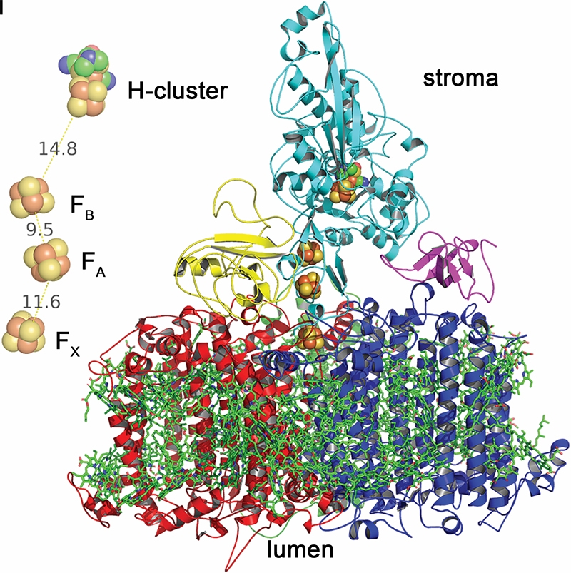
This image was used to illustrate the research,

A model of Photosystem 1 core subunits Courtesy: ASU

Better performing solar cells with newly discovered property of pristine graphene

Light-harvesting devices—I like that better than solar cells or the like but I think that the term serves as a category rather than a name/label for a specific device. Enough musing. A December 17, 2018 news item on Nanowerk describes the latest about graphene and light-harvesting devices (Note: A link has been removed,

An international research team, co-led by a physicist at the University of California, Riverside, has discovered a new mechanism for ultra-efficient charge and energy flow in graphene, opening up opportunities for developing new types of light-harvesting devices.

The researchers fabricated pristine graphene — graphene with no impurities — into different geometric shapes, connecting narrow ribbons and crosses to wide open rectangular regions. They found that when light illuminated constricted areas, such as the region where a narrow ribbon connected two wide regions, they detected a large light-induced current, or photocurrent.

The finding that pristine graphene can very efficiently convert light into electricity could lead to the development of efficient and ultrafast photodetectors — and potentially more efficient solar panels.

A December 14, 2018 University of California at Riverside (UCR) news release by Iqbal Pittalwala (also on EurekAlert but published Dec. 17, 2018), which originated the news item,gives a brief description of graphene while adding context for this research,


Graphene, a 1-atom thick sheet of carbon atoms arranged in a hexagonal lattice, has many desirable material properties, such as high current-carrying capacity and thermal conductivity. In principle, graphene can absorb light at any frequency, making it ideal material for infrared and other types of photodetection, with wide applications in bio-sensing, imaging, and night vision.

In most solar energy harvesting devices, a photocurrent arises only in the presence of a junction between two dissimilar materials, such as “p-n” junctions, the boundary between two types of semiconductor materials. The electrical current is generated in the junction region and moves through the distinct regions of the two materials.

“But in graphene, everything changes,” said Nathaniel Gabor, an associate professor of physics at UCR, who co-led the research project. “We found that photocurrents may arise in pristine graphene under a special condition in which the entire sheet of graphene is completely free of excess electronic charge. Generating the photocurrent requires no special junctions and can instead be controlled, surprisingly, by simply cutting and shaping the graphene sheet into unusual configurations, from ladder-like linear arrays of contacts, to narrowly constricted rectangles, to tapered and terraced edges.”

Pristine graphene is completely charge neutral, meaning there is no excess electronic charge in the material. When wired into a device, however, an electronic charge can be introduced by applying a voltage to a nearby metal. This voltage can induce positive charge, negative charge, or perfectly balance negative and positive charges so the graphene sheet is perfectly charge neutral.

“The light-harvesting device we fabricated is only as thick as a single atom,” Gabor said. “We could use it to engineer devices that are semi-transparent. These could be embedded in unusual environments, such as windows, or they could be combined with other more conventional light-harvesting devices to harvest excess energy that is usually not absorbed. Depending on how the edges are cut to shape, the device can give extraordinarily different signals.”

The research team reports this first observation of an entirely new physical mechanism — a photocurrent generated in charge-neutral graphene with no need for p-n junctions — in Nature Nanotechnology today [Dec. 17, 2018].

Previous work by the Gabor lab showed a photocurrent in graphene results from highly excited “hot” charge carriers. When light hits graphene, high-energy electrons relax to form a population of many relatively cooler electrons, Gabor explained, which are subsequently collected as current. Even though graphene is not a semiconductor, this light-induced hot electron population can be used to generate very large currents.

“All of this behavior is due to graphene’s unique electronic structure,” he said. “In this ‘wonder material,’ light energy is efficiently converted into electronic energy, which can subsequently be transported within the material over remarkably long distances.”

He explained that, about a decade ago, pristine graphene was predicted to exhibit very unusual electronic behavior: electrons should behave like a liquid, allowing energy to be transferred through the electronic medium rather than by moving charges around physically.
“But despite this prediction, no photocurrent measurements had been done on pristine graphene devices — until now,” he said.

The new work on pristine graphene shows electronic energy travels great distances in the absence of excess electronic charge.

The research team has found evidence that the new mechanism results in a greatly enhanced photoresponse in the infrared regime with an ultrafast operation speed.
“We plan to further study this effect in a broad range of infrared and other frequencies, and measure its response speed,” said first author Qiong Ma, a postdoctoral associate in physics at the Massachusetts Institute of Technology, or MIT.

The researchers have provided an image illustrating their work,

Caption: Shining light on graphene: Although graphene has been studied vigorously for more than a decade, new measurements on high-performance graphene devices have revealed yet another unusual property. In ultra-clean graphene sheets, energy can flow over great distances, giving rise to an unprecedented response to light. Credit: Max Grossnickle and QMO Labs, UC Riverside.

Here’s a link to and a citation for the paper,

Giant intrinsic photoresponse in pristine graphene by Qiong Ma, Chun Hung Lui, Justin C. W. Song, Yuxuan Lin, Jian Feng Kong, Yuan Cao, Thao H. Dinh, Nityan L. Nair, Wenjing Fang, Kenji Watanabe, Takashi Taniguchi, Su-Yang Xu, Jing Kong, Tomás Palacios, Nuh Gedik, Nathaniel M. Gabor, & Pablo Jarillo-Herrero. Nature Nanotechnology (2018) Published 17 December 2018 DOI: https://doi.org/10.1038/s41565-018-0323-8

This paper is behind a paywall.

Cyborg bacteria to reduce carbon dioxide

This video is a bit technical but then it is about work being presented to chemists at the American Chemical Society’s (ACS) at the 254th National Meeting & Exposition Aug. 20 -24, 2017,

For a more plain language explanation, there’s an August 22, 2017 ACS news release (also on EurekAlert),

Photosynthesis provides energy for the vast majority of life on Earth. But chlorophyll, the green pigment that plants use to harvest sunlight, is relatively inefficient. To enable humans to capture more of the sun’s energy than natural photosynthesis can, scientists have taught bacteria to cover themselves in tiny, highly efficient solar panels to produce useful compounds.

“Rather than rely on inefficient chlorophyll to harvest sunlight, I’ve taught bacteria how to grow and cover their bodies with tiny semiconductor nanocrystals,” says Kelsey K. Sakimoto, Ph.D., who carried out the research in the lab of Peidong Yang, Ph.D. “These nanocrystals are much more efficient than chlorophyll and can be grown at a fraction of the cost of manufactured solar panels.”

Humans increasingly are looking to find alternatives to fossil fuels as sources of energy and feedstocks for chemical production. Many scientists have worked to create artificial photosynthetic systems to generate renewable energy and simple organic chemicals using sunlight. Progress has been made, but the systems are not efficient enough for commercial production of fuels and feedstocks.

Research in Yang’s lab at the University of California, Berkeley, where Sakimoto earned his Ph.D., focuses on harnessing inorganic semiconductors that can capture sunlight to organisms such as bacteria that can then use the energy to produce useful chemicals from carbon dioxide and water. “The thrust of research in my lab is to essentially ‘supercharge’ nonphotosynthetic bacteria by providing them energy in the form of electrons from inorganic semiconductors, like cadmium sulfide, that are efficient light absorbers,” Yang says. “We are now looking for more benign light absorbers than cadmium sulfide to provide bacteria with energy from light.”

Sakimoto worked with a naturally occurring, nonphotosynthetic bacterium, Moorella thermoacetica, which, as part of its normal respiration, produces acetic acid from carbon dioxide (CO2). Acetic acid is a versatile chemical that can be readily upgraded to a number of fuels, polymers, pharmaceuticals and commodity chemicals through complementary, genetically engineered bacteria.

When Sakimoto fed cadmium and the amino acid cysteine, which contains a sulfur atom, to the bacteria, they synthesized cadmium sulfide (CdS) nanoparticles, which function as solar panels on their surfaces. The hybrid organism, M. thermoacetica-CdS, produces acetic acid from CO2, water and light. “Once covered with these tiny solar panels, the bacteria can synthesize food, fuels and plastics, all using solar energy,” Sakimoto says. “These bacteria outperform natural photosynthesis.”

The bacteria operate at an efficiency of more than 80 percent, and the process is self-replicating and self-regenerating, making this a zero-waste technology. “Synthetic biology and the ability to expand the product scope of CO2 reduction will be crucial to poising this technology as a replacement, or one of many replacements, for the petrochemical industry,” Sakimoto says.

So, do the inorganic-biological hybrids have commercial potential? “I sure hope so!” he says. “Many current systems in artificial photosynthesis require solid electrodes, which is a huge cost. Our algal biofuels are much more attractive, as the whole CO2-to-chemical apparatus is self-contained and only requires a big vat out in the sun.” But he points out that the system still requires some tweaking to tune both the semiconductor and the bacteria. He also suggests that it is possible that the hybrid bacteria he created may have some naturally occurring analog. “A future direction, if this phenomenon exists in nature, would be to bioprospect for these organisms and put them to use,” he says.

For more insight into the work, check out Dexter Johnson’s Aug. 22, 2017 posting on his Nanoclast blog (on the IEEE [Institute of Electrical and Electronics Engineers] website),

“It’s actually a natural, overlooked feature of their biology,” explains Sakimoto in an e-mail interview with IEEE Spectrum. “This bacterium has a detoxification pathway, meaning if it encounters a toxic metal, like cadmium, it will try to precipitate it out, thereby detoxifying it. So when we introduce cadmium ions into the growth medium in which M. thermoacetica is hanging out, it will convert the amino acid cysteine into sulfide, which precipitates out cadmium as cadmium sulfide. The crystals then assemble and stick onto the bacterium through normal electrostatic interactions.”

I’ve just excerpted one bit, there’s more in Dexter’s posting.

Metamaterial could supply air conditioning with zero energy consumption

This is exciting provided they can scale up the metamaterial for industrial use. A Feb. 9, 2017 news item on Nanowerk announces a new metamaterial that could change air conditioning  from the University of Colorado at Boulder (Note: A link has been removed),

A team of University of Colorado Boulder engineers has developed a scalable manufactured metamaterial — an engineered material with extraordinary properties not found in nature — to act as a kind of air conditioning system for structures. It has the ability to cool objects even under direct sunlight with zero energy and water consumption.

When applied to a surface, the metamaterial film cools the object underneath by efficiently reflecting incoming solar energy back into space while simultaneously allowing the surface to shed its own heat in the form of infrared thermal radiation.

The new material, which is described today in the journal Science (“Scalable-manufactured randomized glass-polymer hybrid metamaterial for daytime radiative cooling”), could provide an eco-friendly means of supplementary cooling for thermoelectric power plants, which currently require large amounts of water and electricity to maintain the operating temperatures of their machinery.

A Feb. 9, 2017 University of Colorado at Boulder news release (also on EurekAlert), which originated the news item, expands on the theme (Note: Links have been removed),

The researchers’ glass-polymer hybrid material measures just 50 micrometers thick — slightly thicker than the aluminum foil found in a kitchen — and can be manufactured economically on rolls, making it a potentially viable large-scale technology for both residential and commercial applications.

“We feel that this low-cost manufacturing process will be transformative for real-world applications of this radiative cooling technology,” said Xiaobo Yin, co-director of the research and an assistant professor who holds dual appointments in CU Boulder’s Department of Mechanical Engineering and the Materials Science and Engineering Program. Yin received DARPA’s [US Defense Advanced Research Projects Agency] Young Faculty Award in 2015.

The material takes advantage of passive radiative cooling, the process by which objects naturally shed heat in the form of infrared radiation, without consuming energy. Thermal radiation provides some natural nighttime cooling and is used for residential cooling in some areas, but daytime cooling has historically been more of a challenge. For a structure exposed to sunlight, even a small amount of directly-absorbed solar energy is enough to negate passive radiation.

The challenge for the CU Boulder researchers, then, was to create a material that could provide a one-two punch: reflect any incoming solar rays back into the atmosphere while still providing a means of escape for infrared radiation. To solve this, the researchers embedded visibly-scattering but infrared-radiant glass microspheres into a polymer film. They then added a thin silver coating underneath in order to achieve maximum spectral reflectance.

“Both the glass-polymer metamaterial formation and the silver coating are manufactured at scale on roll-to-roll processes,” added Ronggui Yang, also a professor of mechanical engineering and a Fellow of the American Society of Mechanical Engineers.

“Just 10 to 20 square meters of this material on the rooftop could nicely cool down a single-family house in summer,” said Gang Tan, an associate professor in the University of Wyoming’s Department of Civil and Architectural Engineering and a co-author of the paper.

In addition to being useful for cooling of buildings and power plants, the material could also help improve the efficiency and lifetime of solar panels. In direct sunlight, panels can overheat to temperatures that hamper their ability to convert solar rays into electricity.

“Just by applying this material to the surface of a solar panel, we can cool the panel and recover an additional one to two percent of solar efficiency,” said Yin. “That makes a big difference at scale.”

The engineers have applied for a patent for the technology and are working with CU Boulder’s Technology Transfer Office to explore potential commercial applications. They plan to create a 200-square-meter “cooling farm” prototype in Boulder in 2017.

The invention is the result of a $3 million grant awarded in 2015 to Yang, Yin and Tang by the Energy Department’s Advanced Research Projects Agency-Energy (ARPA-E).

“The key advantage of this technology is that it works 24/7 with no electricity or water usage,” said Yang “We’re excited about the opportunity to explore potential uses in the power industry, aerospace, agriculture and more.”

Here’s a link to and a citation for the paper,

Scalable-manufactured randomized glass-polymer hybrid metamaterial for daytime radiative cooling by Yao Zhai, Yaoguang Ma, Sabrina N. David, Dongliang Zhao, Runnan Lou, Gang Tan, Ronggui Yang, Xiaobo Yin. Science  09 Feb 2017: DOI: 10.1126/science.aai7899

This paper is behind a paywall.

Members of the research team show off the metamaterial (?) Courtesy: University of Colorado at Boulder

I added the caption to this image, which was on the University of Colorado at Boulder’s home page where it accompanied the news release headline on the rotating banner.

Turning gold into see-through rubber for an updated Rumpelstiltskin story

Rumpelstiltskin is a fairy tale whereby a young girl is trapped by her father’s lie that she can spin straw into gold. She is forced to spin gold by the King under pain of execution when an imp offers to help in exchange for various goods. As she succeeds each time, the King demands more until finally she has nothing left to trade for the imp’s help. Well, there is one last thing: her first-born child. She agrees to the bargain and she marries the King. On the birth of their first child, the imp reappears and under pressure of her pleas makes one last bargain. She must guess his name which she does, Rumplestiltskin. (The full story along with variants is here in this Wikipedia entry.)

With this latest research, we have a reverse Rumpelstiltskin story where gold is turned into something else according to a June 13, 2016 news item on Nanowerk (Note: A link has been removed),

Flexible solar panels that could be rolled up for easy transport and other devices would benefit from transparent metal electrodes that can conduct electricity, are stretchable, and resist damage following repeated stretching. Researchers found that topology and the adhesion between a metal nanomesh and the underlying substrate played key roles in creating such materials. The metal nanomesh can be stretched to three times its length while maintaining a transparency comparable to similar commercial materials used in solar cells and flat panel displays. Also, nanomeshes on pre-stretched slippery substrates led to electrodes that didn’t wear out, even after being stretched 50,000 times (Proceedings of the National Academy of Sciences, “Fatigue-free, superstretchable, transparent, and biocompatible metal electrodes”).

Tuning topology and adhesion of metal nanomeshes has led to super stretchable, transparent electrodes that don’t wear out. The scanning electron microscopy image shows the structure of a gold mesh created with a special lithographic technique that controlled the dimensions of the mesh structure. Optimizing this structure and its adhesion to the substrate was key to achieving super stretchability and long lifetimes in use—nanomeshes on pre-stretched slippery substrates did not show signs of wear even after repeated stretching, up to 50,000 cycles.

Tuning topology and adhesion of metal nanomeshes has led to super stretchable, transparent electrodes that don’t wear out. The scanning electron microscopy image shows the structure of a gold mesh created with a special lithographic technique that controlled the dimensions of the mesh structure. Optimizing this structure and its adhesion to the substrate was key to achieving super stretchability and long lifetimes in use—nanomeshes on pre-stretched slippery substrates did not show signs of wear even after repeated stretching, up to 50,000 cycles.

A June 9, 2016 US Dept. of Energy news release,which originated the news item, provides more detail,

Next-generation flexible electronics require highly stretchable and transparent electrodes. Fatigue, structural damage due to repeated use, is deadly in metals as it leads to poor conductivity and it commonly occurs in metals with repeated stretching—even with short elongations. However, few electronic conductors are transparent and stretchable, even fewer can be cyclically stretched to a large strain without causing fatigue. Now researchers led by the University of Houston found that optimizing topology of a metal nanomesh and its adhesion to an underlying substrate improved stretchability and eliminated fatigue, while maintaining transparency. A special lithographic technique called “grain boundary lithography” controlled the dimensions of the mesh structure. The metal nanomesh remained transparent after being stretched to three times its length. Gold nanomeshes on prestretched slippery substrates impressively showed no wear when stretched 50,000 times. The slippery surface advantageously allowed the structure of the nanomesh to reorient to relax the stress. Such electrically conductive, flexible, and transparent electrodes could lead to next-generation flexible electronics such as advanced solar cells.  The nanomesh electrodes are also promising for implantable electronics because the nanomeshes are biocompatible.

Here’s a link to and a citation for the paper,

Fatigue-free, superstretchable, transparent, and biocompatible metal electrodes by Chuan Fei Guo, Qihan Liu, Guohui Wang, Yecheng Wang, Zhengzheng Shi, Zhigang Suo, Ching-Wu Chu, and Zhifeng Ren. Proceedings of the National Academy of Sciences, vol. 112 no. 40,  12332–12337, doi: 10.1073/pnas.1516873112

This paper appears to be open access.

Squeezing light into extremely thin layers

A May 4, 2016 Rice University (US) news release (also on EurekAlert) describes research on molybdenum disulfide and its light absorption properties,

Mechanics know molybdenum disulfide (MoS2) as a useful lubricant in aircraft and motorcycle engines and in the CV and universal joints of trucks and automobiles. Rice University engineering researcher Isabell Thomann knows it as a remarkably light-absorbent substance that holds promise for the development of energy-efficient optoelectronic and photocatalytic devices.

“Basically, we want to understand how much light can be confined in an atomically thin semiconductor monolayer of MoS2,” said Thomann, assistant professor of electrical and computer engineering and of materials science and nanoengineering and of chemistry. “By using simple strategies, we were able to absorb 35 to 37 percent of the incident light in the 400- to 700-nanometer wavelength range, in a layer that is only 0.7 nanometers thick.”

Thomann and Rice graduate students Shah Mohammad Bahauddin and Hossein Robatjazi have recounted their findings in a paper titled “Broadband Absorption Engineering To Enhance Light Absorption in Monolayer MoS2,” which was recently published in the American Chemical Society journal ACS Photonics. The research has many applications, including development of efficient and inexpensive photovoltaic solar panels.

“Squeezing light into these extremely thin layers and extracting the generated charge carriers is an important problem in the field of two-dimensional materials,” she said. “That’s because monolayers of 2-D materials have different electronic and catalytic properties from their bulk or multilayer counterparts.”

Thomann and her team used a combination of numerical simulations, analytical models and experimental optical characterizations. Using three-dimensional electromagnetic simulations, they found that light absorption was enhanced 5.9 times compared with using MoS2 on a sapphire substrate.

“If light absorption in these materials was perfect, we’d be able to create all sorts of energy-efficient optoelectronic and photocatalytic devices. That’s the problem we’re trying to solve,” Thomann said.

She is pleased with her lab’s progress but concedes that much work remains to be done. “The goal, of course, is 100 percent absorption, and we’re not there yet.”

Here’s a link to and a citation for the paper,

Broadband Absorption Engineering to Enhance Light Absorption in Monolayer MoSby Shah Mohammad Bahauddin, Hossein Robatjazi, and Isabell Thomann. ACS Photonics, Article ASAP DOI: 10.1021/acsphotonics.6b00081
Publication Date (Web): April 27, 2016

Copyright © 2016 American Chemical Society

This paper is behind a paywall.

Transparent wood instead of glass for window panes?

The transparent wood is made by removing the lignin in the wood veneer. (Photo: Peter Larsson

The transparent wood is made by removing the lignin in the wood veneer. (Photo: Peter Larsson

Not quite ready as a replacement for some types of glass window panes, nonetheless, transparent (more like translucent) wood is an impressive achievement. According to a March 30, 2016 news item on ScienceDaily size is what makes this piece of transparent wood newsworthy,

Windows and solar panels in the future could be made from one of the best — and cheapest — construction materials known: wood. Researchers at Stockholm’s KTH Royal Institute of Technology [Sweden] have developed a new transparent wood material that’s suitable for mass production.

Lars Berglund, a professor at Wallenberg Wood Science Center at KTH, says that while optically transparent wood has been developed for microscopic samples in the study of wood anatomy, the KTH project introduces a way to use the material on a large scale. …

A March 31 (?), 2016 KTH Institute of Technology press release, which originated the news item, provides more detail,

“Transparent wood is a good material for solar cells, since it’s a low-cost, readily available and renewable resource,” Berglund says. “This becomes particularly important in covering large surfaces with solar cells.”

Berglund says transparent wood panels can also be used for windows, and semitransparent facades, when the idea is to let light in but maintain privacy.

The optically transparent wood is a type of wood veneer in which the lignin, a component of the cell walls, is removed chemically.

“When the lignin is removed, the wood becomes beautifully white. But because wood isn’t not naturally transparent, we achieve that effect with some nanoscale tailoring,” he says.

The white porous veneer substrate is impregnated with a transparent polymer and the optical properties of the two are then matched, he says.

“No one has previously considered the possibility of creating larger transparent structures for use as solar cells and in buildings,” he says

Among the work to be done next is enhancing the transparency of the material and scaling up the manufacturing process, Berglund says.

“We also intend to work further with different types of wood,” he adds.

“Wood is by far the most used bio-based material in buildings. It’s attractive that the material comes from renewable sources. It also offers excellent mechanical properties, including strength, toughness, low density and low thermal conductivity.”

The American Chemical Society has a March 30, 2016 news release about the KTH achievement on EurekAlert  highlighting another potential use for transparent wood,

When it comes to indoor lighting, nothing beats the sun’s rays streaming in through windows. Soon, that natural light could be shining through walls, too. Scientists have developed transparent wood that could be used in building materials and could help home and building owners save money on their artificial lighting costs. …

Homeowners often search for ways to brighten up their living space. They opt for light-colored paints, mirrors and lots of lamps and ceiling lights. But if the walls themselves were transparent, this would reduce the need for artificial lighting — and the associated energy costs. Recent work on making transparent paper from wood has led to the potential for making similar but stronger materials. Lars Berglund and colleagues wanted to pursue this possibility.

Here’s a link to and a citation for the paper,

Optically Transparent Wood from a Nanoporous Cellulosic Template: Combining Functional and Structural Performance by Yuanyuan Li, Qiliang Fu, Shun Yu, Min Yan, and Lars Berglund. Biomacromolecules, Article ASAP DOI: 10.1021/acs.biomac.6b00145 Publication Date (Web): March 4, 2016

Copyright © 2016 American Chemical Society

This paper appears to be open access.

Unboiling egg technology can cut through carbon nanotubes

One of 2015’s big science stories, Flinders University’s ‘egg unboiler’ (also known as, a vortex fluidic device). has made the news again in a March 11, 2016 news item on phys.org,

Technology used by scientists to unboil an egg is being adapted to precisely cut through carbon nanotubes used in solar panel manufacturing and cancer treatment.

Scientists from Flinders University in South Australia have proven their Vortex Fluidic Device’s ability to slice through carbon nanotubes with great precision.

A March 11, 2016 story written by Caleb Radford for The Lead, which originated the news item, notes the advantages to using this technology for slicing carbon nanotubes (CNTs) and prospects for commercialization,

Device creator and Flinders University Professor Colin Raston said the carbon nanotubes could be commercialised within 12 months.

“Importantly for this technology is that we have uniformity in products,” he said.

“It opens it up for applications in drug delivery if you can get all of the carbon nanotubes to about 100 nanometres … 100 nanometres is the ideal length for getting into tumours so you can actually functionalise them to target cancer cells.

“Uniformity in products also means that you can improve the solar cell efficiency in solar cell devices.”

Flinders University scientists last year were awarded an Ig Nobel Award for creating the Vortex Fluidic Device and using it to unboil an egg.

The device can also be used to slice CNTs accurately to an average length of 170 nanometres using only water, a solvent and a laser.

It is also a simpler and cheaper process than previous methods, which resulted in random lengths that made it difficult to deliver drugs to patients and transfer electrons for solar panel manufacturing.

Flinders University PhD student Kasturi Vimalanathan, who played a key role in discovering new applications for the device, said the machines ability to cut carbon nanotubes to a similar length significantly increased the efficiency of solar cells.

“They shorten the carbon nanotubes to fit in all the chemicals so it can withstand high temperatures,” she said.

“It increases the efficiency and enhances the photoelectric conversion because they can provide a shorter transportation pathway for these electrons.

“It’s a one step method we can scale up. We can see cheaper solar panels on the back of this development.”

Here’s an image of Ralston, presumably with his Vortex Fluidic Device,

Professor Colin Raston received global attention and won an Ig Nobel prize on his way to becoming one of the biggest science stories of 2015. Courtesy Flinders University, Australia

Professor Colin Raston received global attention and won an Ig Nobel prize on his way to becoming one of the biggest science stories of 2015. Courtesy Flinders University, Australia

A Dec. 18, 2015 Flinders University blog posting announced Ralston’s Ig Nobel,

When Flinders University’s Professor Colin Raston unboiled an egg earlier this year with his ‘Vortex Fluidic Device’, in a feat previously considered impossible by science, he made TV screens and front pages all over the world, generating a veritable tsunami of ‘eggscellent’ puns.

The global impact of his achievement transformed the softly spoken South Australia Premier’s Professorial Research Fellow in Clean Technology into an internationally recognised figure overnight – and culminated in him receiving a prestigious Ig Nobel prize in September [2015].

In recognition of the massive amount of attention Professor Raston’s achievement received for Australian research, it has today been hailed as one of the top ten weird and wonderful Australian science stories of 2015 by the Australian Science and Media Centre (AusSMC).

Responding to the announcement, Professor Raston said he had been thrilled with the response to his achievement and had been ‘living the dream’ since.

“We were very interested in how the Vortex Fluidic Device might control protein folding, and the breakthrough with my collaborator at UCI, Greg Weiss, simplifies this, in a fraction of the time, minimising waste generation and energy usage. What this amounted to was unboiling an egg,” he said.

Who would have thought a device for unboiling eggs could be used to cut carbon nanotubes? Clearly, Kasturi Vimalanathan. Amazing.

For anyone interested and/or unfamiliar with the Ig Nobel prizes, there’s my Sept. 17, 2013 posting.

South Africa, energy, and nanotechnology

South African academics Nosipho Moloto, Associate Professor, Department of Chemistry, University of the Witwatersrand and Siyabonga P. Ngubane, Lecturer in Chemistry, University of the Witwatersrand have written a Feb. 17, 2016 article for The Conversation (also available on the South African Broadcasting Corporation website) about South Africa’s energy needs and its nanotechnology efforts (Note: Links have been removed),

Energy is an economic driver of both developed and developing countries. South Africa over the past few years has faced an energy crisis with rolling blackouts between 2008 and 2015. Part of the problem has been attributed to mismanagement by the state-owned utility company Eskom, particularly the shortcomings of maintenance plans on several plants.

But South Africa has two things going for it that could help it out of its current crisis. By developing a strong nanotechnology capability and applying this to its rich mineral reserves the country is well-placed to develop new energy technologies.

Nanotechnology has already shown that it has the potential to alleviate energy problems. …

It can also yield materials with new properties and the miniaturisation of devices. For example, since the discovery of graphene, a single atomic layer of graphite, several applications in biological engineering, electronics and composite materials have been identified. These include economic and efficient devices like solar cells and lithium ion secondary batteries.

Nanotechnology has seen an incredible increase in commercialisation. Nearly 10,000 patents have been filed by large corporations since its beginning in 1991. There are already a number of nanotechnology products and solutions on the market. Examples include Miller’s beer bottling composites, Armor’s N-Force line bulletproof vests and printed solar cells produced by Nanosolar – as well as Samsung’s nanotechnology television.

The advent of nanotechnology in South Africa began with the South African Nanotechnology Initiative in 2002. This was followed by the a [sic] national nanotechnology strategy in 2003.

The government has spent more than R450 million [Rand] in nanotechnology and nanosciences research since 2006. For example, two national innovation centres have been set up and funding has been made available for equipment. There has also been flagship funding.

The country could be globally competitive in this field due to the infancy of the technology. As such, there are plenty of opportunities to make novel discoveries in South Africa.

Mineral wealth

There is another major advantage South Africa has that could help diversify its energy supply. It has an abundance of mineral wealth with an estimated value of US$2.5 trillion. The country has the world’s largest reserves of manganese and platinum group metals. It also has massive reserves of gold, diamonds, chromite ore and vanadium.

Through beneficiation and nanotechnology these resources could be used to cater for the development of new energy technologies. Research in beneficiation of minerals for energy applications is gaining momentum. For example, Anglo American and the Department of Science and Technology have embarked on a partnership to convert hydrogen into electricity.

The Council for Scientific and Industrial research also aims to develop low cost lithium ion batteries and supercapacitors using locally mined manganese and titanium ores. There is collaborative researchto use minerals like gold to synthesize nanomaterials for application in photovoltaics.

The current photovoltaic market relies on importing solar cells or panels from Europe, Asia and the US for local assembly to produce arrays. South African UV index is one of the highest in the world which reduces the lifespan of solar panels. The key to a thriving and profitable photovoltaic sector therefore lies in local production and research and development to support the sector.

It’s worth reading the article in its entirety if you’re interested in a perspective on South Africa’s energy and nanotechnology efforts.

Interfaces are the device—organic semiconductors and their edges

Researchers at the University of British Columbia (UBC; Canada) have announced a startling revelation according to an Oct. 6, 2015 news item on ScienceDaily,

As the push for thinner and faster electronics continues, a new finding by University of British Columbia scientists could help inform the design of the next generation of cheaper, more efficient devices.

The work, published this week in Nature Communications, details how electronic properties at the edges of organic molecular systems differ from the rest of the material.

An Oct. 6, 2015 UBC news release on EurekAlert, which originated the news item, expands on the theme,

Organic [as in carbon-based] materials–plastics–are of great interest for use in solar panels, light emitting diodes and transistors. They’re low-cost, light, and take less energy to produce than silicon. Interfaces–where one type of material meets another–play a key role in the functionality of all these devices.

“We found that the polarization-induced energy level shifts from the edge of these materials to the interior are significant, and can’t be neglected when designing components,” says UBC PhD researcher Katherine Cochrane, lead author of the paper.

‘While we were expecting some differences, we were surprised by the size of the effect and that it occurred on the scale of a single molecule,” adds UBC researcher Sarah Burke, an expert on nanoscale electronic and optoelectronic materials and author on the paper.

The researchers looked at ‘nano-islands’ of clustered organic molecules. The molecules were deposited on a silver crystal coated with an ultra-thin layer of salt only two atoms deep. The salt is an insulator and prevents electrons in the organic molecules from interacting with those in the silver–the researchers wanted to isolate the interactions of the molecules.

Not only did the molecules at the edge of the nano-islands have very different properties than in the middle, the variation in properties depended on the position and orientation of other molecules nearby.

The researchers, part of UBC’s Quantum Matter Institute, used a simple, analytical model to explain the differences which can be extended to predict interface properties in much more complex systems, like those encountered in a real device.

Herbert Kroemer said in his Nobel Lecture that ‘The interface is the device’ and it’s equally true for organic materials,” says Burke. [emphasis mine] “The differences we’ve seen at the edges of molecular clusters highlights one effect that we’ll need to consider as we design new materials for these devices, but likely they are many more surprises waiting to be discovered.”

Cochrane and colleagues plan to keep looking at what happens at interfaces in these materials and to work with materials chemists to guide the design rules for the structure and electronic properties of future devices.

Methods

The experiment was performed at UBC’s state-of-the-art Laboratory for Atomic Imaging Research, which features three specially designed ultra-quiet rooms that allow the instruments to sit in complete silence, totally still, to perform their delicate measurements. This allowed the researchers to take dense data sets with a tool called a scanning tunnelling microscope (STM) that showed them the energy levels in real-space on the scale of single atoms.

Here’s a link to and a citation for the paper,

Pronounced polarization-induced energy level shifts at boundaries of organic semiconductor nanostructures by K. A. Cochrane, A. Schiffrin, T. S. Roussy, M. Capsoni, & S. A. Burke. Nature Communications 6, Article number: 8312 doi:10.1038/ncomms9312 Published 06 October 2015

This paper is open access. Yes, I borrowed from Nobel Laureate, Herbert Kroemer for the headline. As Woody Guthrie (legendary American folksinger) once said, more or less, “Only steal from the best.”