Tag Archives: Spanish National Research Council (CSIC)

Graphene-based neural probes

I have two news bits (dated almost one month apart) about the use of graphene in neural probes, one from the European Union and the other from Korea.

European Union (EU)

This work is being announced by the European Commission’s (a subset of the EU) Graphene Flagship (one of two mega-funding projects announced in 2013; 1B Euros each over ten years for the Graphene Flagship and the Human Brain Project).

According to a March 27, 2017 news item on ScienceDaily, researchers have developed a graphene-based neural probe that has been tested on rats,

Measuring brain activity with precision is essential to developing further understanding of diseases such as epilepsy and disorders that affect brain function and motor control. Neural probes with high spatial resolution are needed for both recording and stimulating specific functional areas of the brain. Now, researchers from the Graphene Flagship have developed a new device for recording brain activity in high resolution while maintaining excellent signal to noise ratio (SNR). Based on graphene field-effect transistors, the flexible devices open up new possibilities for the development of functional implants and interfaces.

The research, published in 2D Materials, was a collaborative effort involving Flagship partners Technical University of Munich (TU Munich; Germany), Institut d’Investigacions Biomèdiques August Pi i Sunyer (IDIBAPS; Spain), Spanish National Research Council (CSIC; Spain), The Biomedical Research Networking Center in Bioengineering, Biomaterials and Nanomedicine (CIBER-BBN; Spain) and the Catalan Institute of Nanoscience and Nanotechnology (ICN2; Spain).

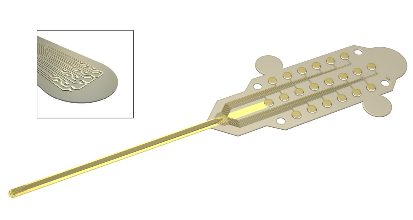
Caption: Graphene transistors integrated in a flexible neural probe enables electrical signals from neurons to be measured with high accuracy and density. Inset: The tip of the probe contains 16 flexible graphene transistors. Credit: ICN2

A March 27, 2017 Graphene Flagship press release on EurekAlert, which originated the news item, describes the work,  in more detail,

The devices were used to record the large signals generated by pre-epileptic activity in rats, as well as the smaller levels of brain activity during sleep and in response to visual light stimulation. These types of activities lead to much smaller electrical signals, and are at the level of typical brain activity. Neural activity is detected through the highly localised electric fields generated when neurons fire, so densely packed, ultra-small measuring devices is important for accurate brain readings.

The neural probes are placed directly on the surface of the brain, so safety is of paramount importance for the development of graphene-based neural implant devices. Importantly, the researchers determined that the graphene-based probes are non-toxic, and did not induce any significant inflammation.

Devices implanted in the brain as neural prosthesis for therapeutic brain stimulation technologies and interfaces for sensory and motor devices, such as artificial limbs, are an important goal for improving quality of life for patients. This work represents a first step towards the use of graphene in research as well as clinical neural devices, showing that graphene-based technologies can deliver the high resolution and high SNR needed for these applications.

First author Benno Blaschke (TU Munich) said “Graphene is one of the few materials that allows recording in a transistor configuration and simultaneously complies with all other requirements for neural probes such as flexibility, biocompability and chemical stability. Although graphene is ideally suited for flexible electronics, it was a great challenge to transfer our fabrication process from rigid substrates to flexible ones. The next step is to optimize the wafer-scale fabrication process and improve device flexibility and stability.”

Jose Antonio Garrido (ICN2), led the research. He said “Mechanical compliance is an important requirement for safe neural probes and interfaces. Currently, the focus is on ultra-soft materials that can adapt conformally to the brain surface. Graphene neural interfaces have shown already great potential, but we have to improve on the yield and homogeneity of the device production in order to advance towards a real technology. Once we have demonstrated the proof of concept in animal studies, the next goal will be to work towards the first human clinical trial with graphene devices during intraoperative mapping of the brain. This means addressing all regulatory issues associated to medical devices such as safety, biocompatibility, etc.”

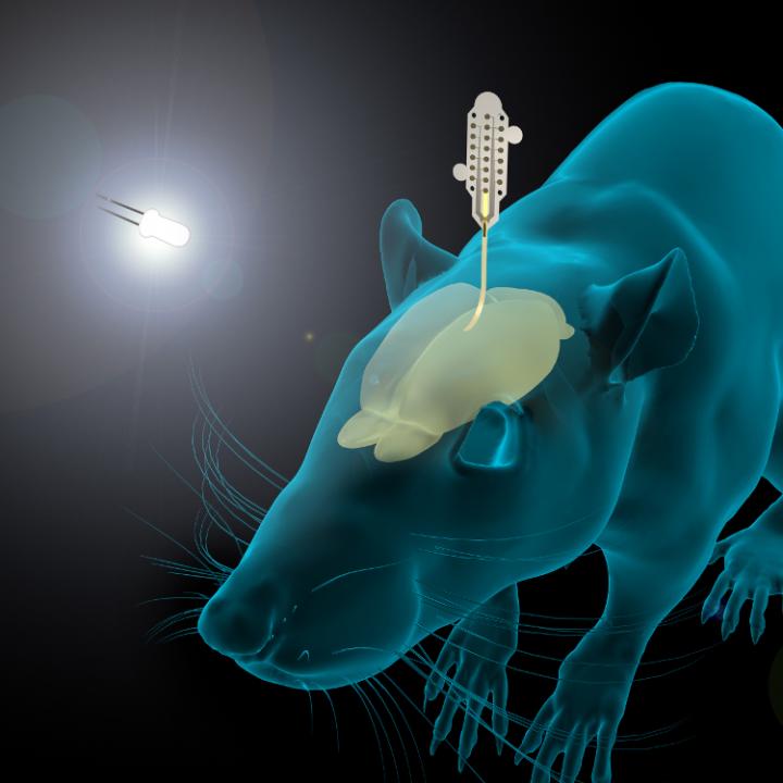
Caption: The graphene-based neural probes were used to detect rats’ responses to visual stimulation, as well as neural signals during sleep. Both types of signals are small, and typically difficult to measure. Credit: ICN2

Here’s a link to and a citation for the paper,

Mapping brain activity with flexible graphene micro-transistors by Benno M Blaschke, Núria Tort-Colet, Anton Guimerà-Brunet, Julia Weinert, Lionel Rousseau, Axel Heimann, Simon Drieschner, Oliver Kempski, Rosa Villa, Maria V Sanchez-Vives. 2D Materials, Volume 4, Number 2 DOI https://doi.org/10.1088/2053-1583/aa5eff Published 24 February 2017

© 2017 IOP Publishing Ltd

This paper is behind a paywall.

Korea

While this research from Korea was published more recently, the probe itself has not been subjected to in vivo (animal testing). From an April 19, 2017 news item on ScienceDaily,

Electrodes placed in the brain record neural activity, and can help treat neural diseases like Parkinson’s and epilepsy. Interest is also growing in developing better brain-machine interfaces, in which electrodes can help control prosthetic limbs. Progress in these fields is hindered by limitations in electrodes, which are relatively stiff and can damage soft brain tissue.

Designing smaller, gentler electrodes that still pick up brain signals is a challenge because brain signals are so weak. Typically, the smaller the electrode, the harder it is to detect a signal. However, a team from the Daegu Gyeongbuk Institute of Science & Technology [DGIST} in Korea developed new probes that are small, flexible and read brain signals clearly.

This is a pretty interesting way to illustrate the research,

Caption: Graphene and gold make a better brain probe. Credit: DGIST

An April 19, 2017 DGIST press release (also on EurekAlert), which originated the news item, expands on the theme (Note: A link has been removed),

The probe consists of an electrode, which records the brain signal. The signal travels down an interconnection line to a connector, which transfers the signal to machines measuring and analysing the signals.

The electrode starts with a thin gold base. Attached to the base are tiny zinc oxide nanowires, which are coated in a thin layer of gold, and then a layer of conducting polymer called PEDOT. These combined materials increase the probe’s effective surface area, conducting properties, and strength of the electrode, while still maintaining flexibility and compatibility with soft tissue.

Packing several long, thin nanowires together onto one probe enables the scientists to make a smaller electrode that retains the same effective surface area of a larger, flat electrode. This means the electrode can shrink, but not reduce signal detection. The interconnection line is made of a mix of graphene and gold. Graphene is flexible and gold is an excellent conductor. The researchers tested the probe and found it read rat brain signals very clearly, much better than a standard flat, gold electrode.

“Our graphene and nanowires-based flexible electrode array can be useful for monitoring and recording the functions of the nervous system, or to deliver electrical signals to the brain,” the researchers conclude in their paper recently published in the journal ACS Applied Materials and Interfaces.

The probe requires further clinical tests before widespread commercialization. The researchers are also interested in developing a wireless version to make it more convenient for a variety of applications.

Here’s a link to and a citation for the paper,

Enhancement of Interface Characteristics of Neural Probe Based on Graphene, ZnO Nanowires, and Conducting Polymer PEDOT by Mingyu Ryu, Jae Hoon Yang, Yumi Ahn, Minkyung Sim, Kyung Hwa Lee, Kyungsoo Kim, Taeju Lee, Seung-Jun Yoo, So Yeun Kim, Cheil Moon, Minkyu Je, Ji-Woong Choi, Youngu Lee, and Jae Eun Jang. ACS Appl. Mater. Interfaces, 2017, 9 (12), pp 10577–10586 DOI: 10.1021/acsami.7b02975 Publication Date (Web): March 7, 2017

Copyright © 2017 American Chemical Society

This paper is behind a paywall.

PlasCarb: producing graphene and renewable hydrogen from food waster

I have two tidbits about PlasCarb the first being an announcement of its existence and the second an announcement of its recently published research. A Jan. 13, 2015 news item on Nanowerk describes the PlasCarb project (Note: A link has been removed),

The Centre for Process Innovation (CPI) is leading a European collaborative project that aims to transform food waste into a sustainable source of significant economic added value, namely graphene and renewable hydrogen.

The project titled PlasCarb will transform biogas generated by the anaerobic digestion of food waste using an innovative low energy microwave plasma process to split biogas (methane and carbon dioxide) into high value graphitic carbon and renewable hydrogen.

A Jan. 13, 2015 CPI press release, which originated the news item, describes the project and its organization in greater detail,

CPI  as the coordinator of the project is responsible for the technical aspects in the separation of biogas into methane and carbon dioxide, and separating of the graphitic carbon produced from the renewable hydrogen. The infrastructure at CPI allows for the microwave plasma process to be trialled and optimised at pilot production scale, with a future technology roadmap devised for commercial scale manufacturing.

Graphene is one of the most interesting inventions of modern times. Stronger than steel, yet light, the material conducts electricity and heat. It has been used for a wide variety of applications, from strengthening tennis rackets, spray on radiators, to building semiconductors, electric circuits and solar cells.

The sustainable creation of graphene and renewable hydrogen from food waste in provides a sustainable method towards dealing with food waste problem that the European Union faces. It is estimated that 90 million tonnes of food is wasted each year, a figure which could rise to approximately 126 million tonnes by 2020. In the UK alone, food waste equates to a financial loss to business of at least £5 billion per year.

Dr Keith Robson, Director of Formulation and Flexible Manufacturing at CPI said, “PlasCarb will provide an innovative solution to the problems associated with food waste, which is one of the biggest challenges that the European Union faces in the strive towards a low carbon economy.  The project will not only seek to reduce food waste but also use new technological methods to turn it into renewable energy resources which themselves are of economic value, and all within a sustainable manner.”

PlasCarb will utilise quality research and specialist industrial process engineering to optimise the quality and economic value of the Graphene and hydrogen, further enhancing the sustainability of the process life cycle.

Graphitic carbon has been identified as one of Europe’s economically critical raw materials and of strategic performance in the development of future emerging technologies. The global market for graphite, either mined or synthetic is worth over €10 billion per annum. Hydrogen is already used in significant quantities by industry and recognised with great potential as a future transport fuel for a low carbon economy. The ability to produce renewable hydrogen also has added benefits as currently 95% of hydrogen is produced from fossil fuels. Moreover, it is currently projected that increasing demand of raw materials from fossil sources will lead to price volatility, accelerated environmental degradation and rising political tensions over resource access.

Therefore, the latter stages of the project will be dedicated to the market uptake of the PlasCarb process and the output products, through the development of an economically sustainable business strategy, a financial risk assessment of the project results and a flexible financial model that is able to act as a primary screen of economic viability. Based on this, an economic analysis of the process will be determined. Through the development of a decentralised business model for widespread trans-European implementation, the valorisation of food waste will have the potential to be undertaken for the benefit of local economies and employment. More specifically, three interrelated post project exploitation markets have been defined: food waste management, high value graphite and RH2 sales.

PlasCarb is a 3-year collaborative project, co-funded under the European Union’s Seventh Framework Programme (FP7) and will further reinforce Europe’s leading position in environmental technologies and innovation in high value Carbon. The consortium is composed of eight partners led by CPI from five European countries, whose complimentary research and industrial expertise will enable the required results to be successfully delivered. The project partners are; The Centre for Process Innovation (UK), GasPlas AS (NO), CNRS (FR), Fraunhofer IBP (DE), Uvasol Ltd (UK), GAP Waste Management (UK), Geonardo Ltd. (HU), Abalonyx AS (NO).

You can find PlasCarb here.

The second announcement can be found in a PlasCarb Jan. 14, 2015 press release announcing the publication of research on heterostructures of graphene ribbons,

Few materials have received as much attention from the scientific world or have raised so many hopes with a view to their potential deployment in new applications as graphene has. This is largely due to its superlative properties: it is the thinnest material in existence, almost transparent, the strongest, the stiffest and at the same time the most strechable, the best thermal conductor, the one with the highest intrinsic charge carrier mobility, plus many more fascinating features. Specifically, its electronic properties can vary enormously through its confinement inside nanostructured systems, for example. That is why ribbons or rows of graphene with nanometric widths are emerging as tremendously interesting electronic components. On the other hand, due to the great variability of electronic properties upon minimal changes in the structure of these nanoribbons, exact control on an atomic level is an indispensable requirement to make the most of all their potential.

The lithographic techniques used in conventional nanotechnology do not yet have such resolution and precision. In the year 2010, however, a way was found to synthesise nanoribbons with atomic precision by means of the so-called molecular self-assembly. Molecules designed for this purpose are deposited onto a surface in such a way that they react with each other and give rise to perfectly specified graphene nanoribbons by means of a highly reproducible process and without any other external mediation than heating to the required temperature. In 2013 a team of scientists from the University of Berkeley and the Centre for Materials Physics (CFM), a mixed CSIC (Spanish National Research Council) and UPV/EHU (University of the Basque Country) centre, extended this very concept to new molecules that were forming wider graphene nanoribbons and therefore with new electronic properties. This same group has now managed to go a step further by creating, through this self-assembly, heterostructures that blend segments of graphene nanoribbons of two different widths.

The forming of heterostructures with different materials has been a concept widely used in electronic engineering and has enabled huge advances to be made in conventional electronics. “We have now managed for the first time to form heterostructures of graphene nanoribbons modulating their width on a molecular level with atomic precision. What is more, their subsequent characterisation by means of scanning tunnelling microscopy and spectroscopy, complemented with first principles theoretical calculations, has shown that it gives rise to a system with very interesting electronic properties which include, for example, the creation of what are known as quantum wells,” pointed out the scientist Dimas de Oteyza, who has participated in this project. This work, the results of which are being published this very week in the journal Nature Nanotechnology, therefore constitutes a significant success towards the desired deployment of graphene in commercial electronic applications.

Here’s a link to and a citation for the paper,

Molecular bandgap engineering of bottom-up synthesized graphene nanoribbon heterojunctions by Yen-Chia Chen, Ting Cao, Chen Chen, Zahra Pedramrazi, Danny Haberer, Dimas G. de Oteyza, Felix R. Fischer, Steven G. Louie, & Michael F. Crommie. Nature Nanotechnology (2015) doi:10.1038/nnano.2014.307 Published online 12 January 2015

This article is behind a paywall but there is a free preview available via ReadCube access.