Tag Archives: SungWoo Nam

Crumpling graphene to create a 3D structure and reflattening it afterwards

The reseaarchers at the University of Illinois College of Engineering are quite excited about a new technique for crumpling graphene as a Feb. 17, 2015 news item on ScienceDaily reports,

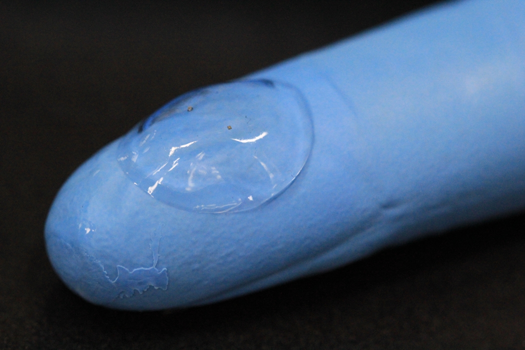
Researchers at the University of Illinois at Urbana-Champaign have developed a unique single-step process to achieve three-dimensional (3D) texturing of graphene and graphite. Using a commercially available thermally activated shape-memory polymer substrate, this 3D texturing, or “crumpling,” allows for increased surface area and opens the doors to expanded capabilities for electronics and biomaterials.

“Fundamentally, intrinsic strains on crumpled graphene could allow modulation of electrical and optical properties of graphene,” explained SungWoo Nam, an assistant professor of mechanical science and engineering at Illinois. “We believe that the crumpled graphene surfaces can be used as higher surface area electrodes for battery and supercapacitor applications. As a coating layer, 3D textured/crumpled nano-topographies could allow omniphobic/anti-bacterial surfaces for advanced coating applications.”

A Feb. 16, 2015 University of Illinois College of Engineering news release (also on EurekAlert), which originated the news item, describes the nature of graphene and what makes this technique so exciting,

Graphene—a single atomic layer of sp2-bonded carbon atoms—has been a material of intensive research and interest over recent years.  A combination of exceptional mechanical properties, high carrier mobility, thermal conductivity, and chemical inertness, make graphene a prime candidate material for next generation optoelectronic, electromechanical, and biomedical applications.

“In this study, we developed a novel method for controlled crumpling of graphene and graphite via heat-induced contractile deformation of the underlying substrate,” explained Michael Cai Wang, a graduate student and first author of the paper, “Heterogeneous, Three-Dimensional Texturing of Graphene,” which appeared in the journal Nano Letters. ”While graphene intrinsically exhibits tiny ripples in ambient conditions, we created large and tunable crumpled textures in a tailored and scalable fashion.”

“As a simpler, more scalable, and spatially selective method, this texturing of graphene and graphite exploits the thermally induced transformation of shape-memory thermoplastics, which has been previously applied to microfluidic device fabrication, metallic  film patterning, nanowire assembly, and robotic self-assembly applications,” added Nam, whose group has filed a patent for their novel strategy. “The thermoplastic nature of the polymeric substrate also allows for the crumpled graphene morphology to be arbitrarily re-flattened at the same elevated temperature for the crumpling process.”

“Due to the extremely low cost and ease of processing of our approach, we believe that this will be a new way to manufacture nanoscale topographies for graphene and many other 2D and thin-film materials.”

The researchers are also investigating the textured graphene surfaces for 3D sensor applications.

“Enhanced surface area will allow even more sensitive and intimate interactions with biological systems, leading to high sensitivity devices,” Nam said.

The funding agencies for this project were unexpectedly interesting (to me), from the news release,

Funding for this research was provided through the Air Force Office for Scientific Research, American Chemical Society and Brain Research Foundation. [emphasis mine] In addition to Wang, co-authors from Nam’s research group at Illinois include SungGyu Chun, Ryan Han, Ali Ashraf, and Pilgyu Kang.

Here’s a link to and a citation for the paper,

Heterogeneous, Three-Dimensional Texturing of Graphene by Michael Cai Wang, SungGyu Chun, Ryan Steven Han, Ali Ashraf, Pilgyu Kang, and SungWoo Nam. Nano Lett., Article ASAP
DOI: 10.1021/nl504612y Publication Date (Web): February 10, 2015

Copyright © 2015 American Chemical Society

This paper is behind a paywall.

Dexter Johnson has written a Feb. 20, 2015 post highlighting this work on his Nanoclast blog (on the Institute of Electrical and Electronics Engineers [IEEE] website).

Shrinky Dinks* instrumental for new nanowires technique

Shrinky Dinks, a material used for children’s arts and crafts projects, has proved instrumental for developing a new technique to close the gap between nanowires. From a July 1, 2014 news item on Nanowerk (Note: A link has been removed),

How do you put a puzzle together when the pieces are too tiny to pick up? Shrink the distance between them.

Engineers at the University of Illinois at Urbana-Champaign are using Shrinky Dinks, plastic that shrinks under high heat, to close the gap between nanowires in an array to make them useful for high-performance electronics applications. The group published its technique in the journal Nano Letters (“Assembly and Densification of Nanowire Arrays via Shrinkage”).

A July 1, 2014 University of Illinois at Urbana-Champaign news release, which originated the news item, provides more details about the new technique,

Nanowires are extremely fast, efficient semiconductors, but to be useful for electronics applications, they need to be packed together in dense arrays. Researchers have struggled to find a way to put large numbers of nanowires together so that they are aligned in the same direction and only one layer thick.

“Chemists have already done a brilliant job in making nanowires exhibit very high performance. We just don’t have a way to put them into a material that we can handle,” said study leader SungWoo Nam, a professor of mechanical science and engineering at the U. of I. “With the shrinking approach, people can make nanowires and nanotubes using any method they like and use the shrinking action to compact them into a higher density.”

The researchers place the nanowires on the Shrinky Dinks plastic as they would for any other substrate, but then shrink it to bring the wires much closer together. This allows them to create very dense arrays of nanowires in a simple, flexible and very controllable way.

The shrinking method has the added bonus of bringing the nanowires into alignment as they increase in density. Nam’s group demonstrated how even wires more than 30 degrees off-kilter can be brought into perfect alignment with their neighbors after shrinking.

“There’s assembly happening at the same time as the density increases,” Nam said, “so even if the wires are assembled in a disoriented direction we can still use this approach.”

The plastic is clamped before baking so that it only shrinks in one direction, so that the wires pack together but do not buckle. Clamping in different places could direct the arrays into interesting formations, according to Nam. The researchers also can control how densely the wires pack by varying the length of time the plastic is heated. They also are exploring using lasers to precisely shrink the plastic in specific patterns.

Nam first had the idea for using Shrinky Dinks plastic to assemble nanomaterials after seeing a microfluidics device that used channels made of shrinking plastic. He realized that the high degree of shrinking and the low cost of plastic could have a huge impact on nanowire assembly and processing for applications.

“I’m interested in this concept of synthesizing new materials that are assembled from nanoscale building blocks,” Nam said. “You can create new functions. For example, experiments have shown that film made of packed nanowires has properties that differ quite a bit from a crystal thin film.”

One application the group is now exploring is a thin film solar cell, made of densely packed nanowires, that could harvest energy from light much more efficiently than traditional thin-film solar cells.

I have featured the Shrinky Dinks product and its use for nanoscale fabrication before in an Aug. 16, 2010 posting which featured this reply from the lead researcher for that project on nanopatterning,

ETA Aug.17.10: I also contacted Teri W. Odom, professor at Northwestern University about why they use Slinky Dinks in their work. She very kindly responded with this:

Part of what we are interested in is the development of low-cost nanofabrication tools that can create macroscale areas of nanoscale patterns in a single step. For a variety of reasons, this end-product is hard to obtain—even though we and others have chipped away at this problem for years.

As an example, to achieve smaller and smaller separations between patterns, either expensive, top-down serial tools (such as electron beam lithography or scanning probe techniques) or bottom-up assembly methods need to be used. However, the former cannot easily create large areas of patterns, and the latter cannot readily control the separations of patterns.

We needed a way to obtain nanopatterns separated by specific distances on-demand. Here is where the Shrinky Dinks material comes in. My student had read a paper (published in 2007 in Lab on a Chip) about how this material was used to make microscale patterns starting from a pattern printed using a laser printer. I imagine his thought was: if this material could be used for microscale patterns, why not for nanoscale ones? It would be cheap, and it’s easy to order.

So, we combined this substrate with our new molding method—solvent assisted nanoscale embossing (SANE)—and could now heat the material to shrink the spacing between patterns. And thus, in some sense, we made available to any lab some of the capabilities of the billion-dollar nanofabrication industry for less than one-hundred dollars.

Getting back to this latest use of Shrinky Dinks, here’s a link to and a citation for the ‘nanowires’ research paper,

Assembly and Densification of Nanowire Arrays via Shrinkage by Jaehoon Bang, Jonghyun Choi, Fan Xia, Sun Sang Kwon, Ali Ashraf, Won Il Park, and SungWoo Nam. Nano Lett., 2014, 14 (6), pp 3304–3308 DOI: 10.1021/nl500709p Publication Date (Web): May 16, 2014
Copyright © 2014 American Chemical Society

This paper is behind a paywall.

* ‘dinks’ in headline changed to ‘Dinks’ on July 2, 2014 at 1150 hours PDT.

LEDs for your contact lenses from Korea’s Ulsan National Institute of Science and Technology

Probably the most exciting application for this work from Korea is where stretchable graphene-metal nanowire electrodes can be fitted to soft contact lenses paving the way for picture-taking and scanning lenses. A May 30, 2013 news item on Nanowerk describes the research in broad terms (Note: A link has been removed),

A hybrid transparent and stretchable electrode could open the new way for flexible displays, solar cells, and even electronic devices fitted on a curvature substrate such as soft eye contact lenses, by the UNIST (Ulsan National Institute of Science and Technology) research team (“High-Performance, Transparent, and Stretchable Electrodes Using Graphene–Metal Nanowire Hybrid Structures”).

The UNIST May 31, 2013 news release by Eunhee Song about the research provides context and detail,

Transparent electrodes are in and of themselves nothing all that new – they have been widely used in things like touch screens, flat-screen TVs, solar cells and light-emitting devices. Currently transparent electrodes are commonly made from a material known as indium tin oxide (ITO). Although it suffices for its job, it’s brittle, cracking and losing functionality if flexed. It also degrades over time, and is somewhat expensive due to the limited quantities of indium metal.

As an alternative, the networks of randomly distributed mNWs [metal nanowires] have been considered as promising candidates for next-generation transparent electrodes, due to their low-cost, high-speed fabrication of transparent electrodes.

However, the number of disadvantage of the mNW networks has limited their integration into commercial devices. They have low breakdown voltage, typically high NW-NW junction resistance, high contact resistance between network and active materials, material instability and poor adhesion to plastic substrates.

UNIST scientists here, combined graphene with silver nanowires to form a thin, transparent and stretchable electrode. Combining graphene and silver nanowires in a hybrid material overcomes weakness of individual material.

Graphene is also well known as good a candidate for transparent electrode because of their unique electrical properties and high mechanical flexibility. However, scalable graphene synthesis methods for commercialization produces lower quality graphene with individual segments called grains which increases the electrical resistance at boundaries between these grains.

Silver nanowires, on the other hand, have high resistance because they are randomly oriented like a jumble of toothpicks facing in different directions. In this random orientation, there are many contact between nanowires, resulting in high resistance due to large junction resistance of nanowires. Due to these drawbacks, neither is good for conducting electricity, but a hybrid structure, combined from two materials, is.

As a result, it presents a high electrical and optical performance with mechanical flexibility and stretchability for flexible electronics. The hybrid Transparent electrode reportedly has a low “sheet resistance” while preserving high transmittance. There’s almost no change in its resistance when bent and folded where ITO is bent, its resistance increases significantly. Additionally the hybrid material reportedly has a low “sheet resistance” while preserving electrical and optical properties reliable against thermal oxidation condition

The graphene-mNW hybrid structure developed by the research team, as a new class of such electrodes, may soon find use in a variety of other applications. The research team demonstrated Inorganic light-emitting diode (ILDED) devices fitted on a soft eye contact lens using the transparent, stretchable interconnects of the hybrid electrodes as an application example.

Here are some images from the research team,

Hybrid transparent and stretchable electrode as part of norganic light-emitting diode (ILDED) devices fitted on a soft eye contact lens. Image courtesy of  Korea's UNIST(Ulsan National Institute of Science and Technology)

Hybrid transparent and stretchable electrode as part of norganic light-emitting diode (ILDED) devices fitted on a soft eye contact lens. Image courtesy of Korea’s UNIST (Ulsan National Institute of Science and Technology)

There has already been an in vivo study of the ‘electrified’ soft contact lens (from the news release),

As an in vivo study, this contact lens was worn by a live rabbit eye for five hours and none of abnormal behavior, such as bloodshot eye or the rubbing of eye areas, of the live rabbit had been observed.

Wearing eye contact lenses, picture-taking and scanning, is not a scene on Sci-Fi movie anymore.

Jang-Ung Park, professor of the School of Nano-Bioscience and Chemical Engineering, UNIST, led the effort.

“We believe the hybridization between two-dimensional and one-dimensional nanomaterials presents a promising strategy toward flexible, wearable electronics and implantable biosensor devices, and indicate the substantial promise of future electronics,” said Prof. Park.

Here’s a close-up of a test bunny’s eye,

Rabbit's (bunny's) eye with Inorganic light-emitting diode (ILDED) devices fitted on a soft eye contact lens (using the transparent, stretchable interconnects of the hybrid electrodes).  Courtesy of UNIST (Ulsan National Institute of Science and Technology)

Rabbit’s (bunny’s) eye with Inorganic light-emitting diode (ILDED) devices fitted on a soft eye contact lens (using the transparent, stretchable interconnects of the hybrid electrodes).
Courtesy of UNIST (Ulsan National Institute of Science and Technology)

I wonder how one would control the picture-taking, scanning capabilities. In any event, here’s a link to and a citation for the research paper,

High-Performance, Transparent, and Stretchable Electrodes Using Graphene–Metal Nanowire Hybrid Structures by Mi-Sun Lee, Kyongsoo Lee, So-Yun Kim, Heejoo Lee, Jihun Park, Kwang-Hyuk Choi, Han-Ki Kim, Dae-Gon Kim, Dae-Young Lee, SungWoo Nam, and Jang-Ung Park. Nano Lett. [Nano Letters], Article ASAP DOI: 10.1021/nl401070p Publication Date (Web): May 23, 2013

Copyright © 2013 American Chemical Society

This paper is behind a paywall.