As amazing as the altar appears, it was hiding some even more amazing secrets. From an October 10, 2022 Paul Scherrer Institute (PSI) press release (also on EurekAlert but published October 11, 2022) by Barbara Vonarburg,
To gild sculptures in the late Middle Ages, artists often applied ultra-thin gold foil supported by a silver base layer. For the first time, scientists at the Paul Scherrer Institute [PSI] have managed to produce nanoscale 3D images of this material, known as Zwischgold. The pictures show this was a highly sophisticated mediaeval production technique and demonstrate why restoring such precious gilded artefacts is so difficult.
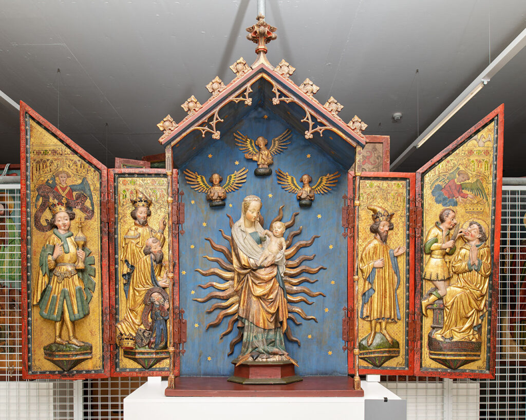
The samples examined at the Swiss Light Source SLS using one of the most advanced microscopy methods were unusual even for the highly experienced PSI team: minute samples of materials taken from an altar and wooden statues originating from the fifteenth century. The altar is thought to have been made around 1420 in Southern Germany and stood for a long time in a mountain chapel on Alp Leiggern in the Swiss canton of Valais. Today it is on display at the Swiss National Museum (Landesmuseum Zürich). In the middle you can see Mary cradling Baby Jesus. The material sample was taken from a fold in the Virgin Mary’s robe. The tiny samples from the other two mediaeval structures were supplied by Basel Historical Museum.
The material was used to gild the sacred figures. It is not actually gold leaf, but a special double-sided foil of gold and silver where the gold can be ultra-thin because it is supported by the silver base. This material, known as Zwischgold (part-gold) was significantly cheaper than using pure gold leaf. “Although Zwischgold was frequently used in the Middle Ages, very little was known about this material up to now,” says PSI physicist Benjamin Watts: “So we wanted to investigate the samples using 3D technology which can visualise extremely fine details.” Although other microscopy techniques had been used previously to examine Zwischgold, they only provided a 2D cross-section through the material. In other words, it was only possible to view the surface of the cut segment, rather than looking inside the material. The scientists were also worried that cutting through it may have changed the structure of the sample. The advanced microscopy imaging method used today, ptychographic tomography, provides a 3D image of Zwischgold’s exact composition for the first time.
X-rays generate a diffraction pattern
The PSI scientists conducted their research using X-rays produced by the Swiss Light Source SLS. These produce tomographs displaying details in the nanoscale range – millionths of a millimetre, in other words. “Ptychography is a fairly sophisticated method, as there is no objective lens that forms an image directly on the detector,” Watts explains. Ptychography actually produces a diffraction pattern of the illuminated area, in other words an image with points of differing intensity. By manipulating the sample in a precisely defined manner, it is possible to generate hundreds of overlapping diffraction patterns. “We can then combine these diffraction patterns like a sort of giant Sudoku puzzle and work out what the original image looked like,” says the physicist. A set of ptychographic images taken from different directions can be combined to create a 3D tomogram.
The advantage of this method is its extremely high resolution. “We knew the thickness of the Zwischgold sample taken from Mary was of the order of hundreds of nanometres,” Watts explains. “So we had to be able to reveal even tinier details.” The scientists achieved this using ptychographic tomography, as they report in their latest article in the journal Nanoscale. “The 3D images clearly show how thinly and evenly the gold layer is over the silver base layer,” says Qing Wu, lead author of the publication. The art historian and conservation scientist completed her PhD at the University of Zurich, in collaboration with PSI and the Swiss National Museum. “Many people had assumed that technology in the Middle Ages was not particularly advanced,” Wu comments. “On the contrary: this was not the Dark Ages, but a period when metallurgy and gilding techniques were incredibly well developed.”
Secret recipe revealed
Unfortunately there are no records of how Zwischgold was produced at the time. “We reckon the artisans kept their recipe secret,” says Wu. Based on nanoscale images and documents from later epochs, however, the art historian now knows the method used in the 15th century: first the gold and the silver were hammered separately to produce thin foils, whereby the gold film had to be much thinner than the silver. Then the two metal foils were worked on together. Wu describes the process: “This required special beating tools and pouches with various inserts made of different materials into which the foils were inserted,” Wu explains. This was a fairly complicated procedure that required highly skilled specialists.
“Our investigations of Zwischgold samples showed the average thickness of the gold layer to be around 30 nanometres, while gold leaf produced in the same period and region was approximately 140 nanometres thick,” Wu explains. “This method saved on gold, which was much more expensive”. At the same time, there was also a very strict hierarchy of materials: gold leaf was used to make the halo of one figure, for example, while Zwischgold was used for the robe. Because this material has less of a sheen, the artists often used it to colour the hair or beards of their statues. “It is incredible how someone with only hand tools was able to craft such nanoscale material,” Watts says. Mediaeval artisans also benefited from a unique property of gold and silver crystals when pressed together: their morphology is preserved across the entire metal film. “A lucky coincidence of nature that ensures this technique works,” says the physicist.
Golden surface turns black
The 3D images do bring to light one drawback of using Zwischgold, however: the silver can push through the gold layer and cover it. The silver moves surprisingly quickly – even at room temperature. Within days, a thin silver coating covers the gold completely. At the surface the silver comes into contact with water and sulphur in the air, and corrodes. “This makes the gold surface of the Zwischgold turn black over time,” Watts explains. “The only thing you can do about this is to seal the surface with a varnish so the sulphur does not attack the silver and form silver sulphide.” The artisans using Zwischgold were aware of this problem from the start. They used resin, glue or other organic substances as a varnish. “But over hundreds of years this protective layer has decomposed, allowing corrosion to continue,” Wu explains.
The corrosion also encourages more and more silver to migrate to the surface, creating a gap below the Zwischgold. “We were surprised how clearly this gap under the metal layer could be seen,” says Watts. Especially in the sample taken from Mary’s robe, the Zwischgold had clearly come away from the base layer. “This gap can cause mechanical instability, and we expect that in some cases it is only the protective coating over the Zwischgold that is holding the metal foil in place,” Wu warns. This is a massive problem for the restoration of historical artefacts, as the silver sulphide has become embedded in the varnish layer or even further down. “If we remove the unsightly products of corrosion, the varnish layer will also fall away and we will lose everything,” says Wu. She hopes it will be possible in future to develop a special material that can be used to fill the gap and keep the Zwischgold attached. “Using ptychographic tomography, we could check how well such a consolidation material would perform its task,” says the art historian.
About PSI
The Paul Scherrer Institute PSI develops, builds and operates large, complex research facilities and makes them available to the national and international research community. The institute’s own key research priorities are in the fields of matter and materials, energy and environment and human health. PSI is committed to the training of future generations. Therefore about one quarter of our staff are post-docs, post-graduates or apprentices. Altogether PSI employs 2100 people, thus being the largest research institute in Switzerland. The annual budget amounts to approximately CHF 400 million. PSI is part of the ETH Domain, with the other members being the two Swiss Federal Institutes of Technology, ETH Zurich and EPFL Lausanne, as well as Eawag (Swiss Federal Institute of Aquatic Science and Technology), Empa (Swiss Federal Laboratories for Materials Science and Technology) and WSL (Swiss Federal Institute for Forest, Snow and Landscape Research). Insight into the exciting research of the PSI with changing focal points is provided 3 times a year in the publication 5232 – The Magazine of the Paul Scherrer Institute.
Here’s a link to and a citation for the paper,
A modern look at a medieval bilayer metal leaf: nanotomography of Zwischgold by
Qing Wu, Karolina Soppa, Elisabeth Müller, Julian Müller, Michal Odstrcil, Esther Hsiao Rho Tsai, Andreas Späth, Mirko Holler, Manuel Guizar-Sicairos, Benjamin Butz, Rainer H. Fink, and Benjamin Watts. Nanoscale DOI: https://doi.org/10.1039/D2NR03367D First published: 10 Oct 2022
This paper is open access.