There are three inter-related nanotechnology-themed events taking place in Ireland starting today, Sept. 14, 2012 with the twin launches of Nanoweek 2012, which runs until Sept. 21, 2012, and a preview of the Magical Materials exhibition, which runs Sept. 15 – Oct. 14, 2012, at Trinity College Dublin’s (TCD) Science Gallery.
During Nanoweek 2012, which is hosted by NanoNet Ireland, the third inter-related event, which as it turns out, is the organization’s 3rd national nanotechnology conference and that will be held Sept. 17 – 18, 2012 at Trinity College Dublin. Details here.
The Sept. 13, 2012 news item on Nanowerk provides more detail about the Magical Materials exhibit,
CRANN [Centre for Research on Adaptive Nanostructures and Nanodevices], the Science Foundation Ireland funded nanoscience institute based at Trinity College Dublin, today celebrated the launch of Nanoweek 2012 with the opening of a new exhibition jointly developed with Science Gallery. Magical Materials is a free, month long show at Science Gallery which explores the peculiar properties of the world’s most futuristic and spectacular materials. Visitors to the exhibition will have a chance to see, touch and experience almost fifty Magical Materials including:
Aerogel, the lightest solid in the world (dubbed ‘solid smoke’)
Graphene, a layer of graphite just one atom thick but 200 times stronger than steel
Smart textiles that store information, keep your gadgets charged and raise oxygen levels in blood.
The Sept. 13, 2012 news release from CRANN (which originated the news item) provides some insight into how nanotechnology’s importance in Ireland,
Speaking at the Magical Materials exhibition, Dr. Diarmuid O’Brien, Executive Director of CRANN said, “The hugely significant impact of nanoscience and material science on our everyday lives is such that general and widespread understanding of its reach is crucial. Nanoweek 2012, through “Magical Materials” brings the impact of this research to life in a very tangible way for the public. Nanoscience is a crucial contributor to the Irish economy. It is linked to 120,000 jobs, totalling 10% of our annual exports or €15 billion across a range of sectors including medicine, pharmaceuticals, technology and energy. Science Gallery has an impressive track record of attracting large numbers of young visitors to their exhibitions and we are delighted to have collaborated with them on this month long exhibition, We hope that this event will lead to a growing awareness of the importance of nanoscience to Ireland”.
As for the Magical Materials*; Unleash Your Superpowers exhibit itself, here’s more, from the exhibition webpage,
What makes a material magical? An ability to change shape before your eyes, to turn from a liquid to a solid or to be one of the lightest materials on earth and yet also one of the strongest? MAGICAL MATERIALS explores the properties of some of the world’s most mysterious materials, giving you an opportunity to investigate and experiment at the cutting edge of material science.
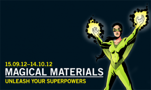
Six nanotechnology superheroes have been created for this, here’s Florogirl,

Floro Girl by Stephen Byrne for Trinity College Dublin’s Science Gallery ‘Magic Materials’ exhibition.
I love the description of how and why this superhero was created,
The sixth and final superhero comic book cover in artist Stephen Byrne’s MAGICAL MATERIALS-inspired series sees him bringing to life a category of materials called Designed By Nature [aka biomimicry].
…
Inspired by artificial photosynthesis, Stephen imagined an investigative reporter who had accidentally exposed herself to nickel-molybdenum-zinc, and found herself able to imitate the process of photosynthesis by converting light from the sun and moisture from the air into energy, and named her Florogirl. Florogirl can use her powers to create highly concentrated energy beams, and while she can store up energy, she runs the risk of running out of her energy reserves at night.…
Nickel-molybdenum-zinc is a compound used in manufacturing ‘artificial leaves’. Resembling thin playing cards, when covered with water and placed in sunlight, artificial leaves go through a biomimetic process that replicates capturing sunlight energy, water and carbon dioxide and converting them into carbohydrates and oxygen. This mimics photosynthesis, an efficient way of turning sunlight into energy, and replaces nature’s use of pigments such as chlorophyll.
I recommend visiting the Florogirl page where there is a video about artificial leaves, links to other resources, and links to more nanotechnology superheroes created by Byrne.
Concurrent with these nanotechnology-themed events, the Science Gallery is presenting a related project, Let’s Make Stuff, and associated events. The glue binding together the nanotechnology theme and ‘making stuff’ theme is the emphasis on materials. From the CRANN news release,
As part of Magical Materials ‘Director of Stuff, Producer of Things, Maker of Objects and Collector of Materials’, Zoe Loughlin, will present ‘Performativity of Matter’ on the 18th September, while Mark Miodownik from the Institute of Making will speak on September 27th. During the exhibition, Science Gallery will also explore science fiction in ‘From Grey Goo to Tricorders – How Science Fiction Influences Reality’ and bring back the hugely successful Curated Dinner series for members.
Sadly, I was not able to find any information about the ‘From Grey Goo to Tricorders – How Science Fiction Influences Reality’ event but perhaps they haven’t been able to schedule it yet. In the meantime, here’s a little more about the ‘Performativity of Matter’, from the event page (where you can book a ticket for this talk),
“First presented in 2008 at the ICA [Institute of Contemporary Art] in London, this ‘science demonstration lecture performance’ spotlights the performing nature – or performativity – of materials. As Zoe explains, performance isn’t just about animate objects – inanimate objects perform, too. This ever-evolving piece first emerged after a successful work by Zoe in which she gave a performance lecture about a mathematical equation she discovered. Since then, Zoe has been invited to perform around the UK and Europe to all manner of audiences. For example, last year saw her devise a lecture performance show on liquids for the Fundus Theatre in Germany.
Importantly, “The Performativity of Matter” is never the same twice. It is responsive to each diverse audience and setting, taking into account that the main performers on the stage – the materials – can’t always be controlled. But, to use one of Zoe’s expressions, if an on-stage demonstration works as it should on stage, it’s science. If it doesn’t, it’s art.”
Zoe Laughlin is a co-founder/director of the Institute of Making and the Materials Library project. She holds an MA from Central Saint Martin’s College of Art and Design and obtained a PhD in Materials within the Division of Engineering, King’s College London. Working at the interface of the science, art, craft and design of materials, her work ranges from formal experiments with matter, to materials consultancy and large-scale public exhibitions and events with partners including Tate Modern, the Hayward Gallery, the V&A Museum, the Science Museum and the Wellcome Collection.
A Q&A session will follow Zoe’s talk
The Science Gallery currently has opened a popup shop under its Let’s Make Stuff banner, from the Science Gallery home page,
MAKESHOP — a pop-up experiment by Science Gallery, is a new collaborative workshop space where you can learn everything from cross-stitching to DIY robotics.
One last item on the ‘making stuff’ theme, Mark Miodownick’s talk on Sept. 27, 2012, from the event page (where you can book a ticket),
Whatever people think about the rapid pace of change in the past, the fundamental arrangement of materials on the planet has not altered. There are living things which we call life, and there are non-living things which we call rocks, tools, buildings and so on. As a result of our greater understanding of matter, this distinction is now becoming blurred and is likely to usher in a new materials age.
Mark Miodownik, from the Institute of Making, believes bionic people with synthetic organs, bones and even brains will be the norm. Just as we become more synthetic, so our man-made environment is changing to become more lifelike: living buildings, and objects that heal-themselves are on the horizon.
His talk will review the imminent changes to the material world that are coming our way, and a Q&A session will follow.
Hats off to the Science Gallery, CRANN, TCD, and NanoNet Ireland, this looks to be a very exciting set of programmes engaging experts and the public in a variety of ways and means. I’d dearly love to know if anyone is analyzing these various initiatives for their impact on public awareness and understanding of nanotechnology and materials.
*’Mateirals’ corrected to ‘Materials’ on Nov. 7, 2014.
