A Feb. 29, 2016 news item on ScienceDaily announces a new development concerning free radicals that may be helpful with skin diseases and pathologies,
Researchers at The Hebrew University of Jerusalem have developed a nanotechnology-based delivery system containing a protective cellular pathway inducer that activates the body’s natural defense against free radicals efficiently, a development that could control a variety of skin pathologies and disorders.
A Feb. 29, 2016 Hebrew University of Jerusalem press release on EurekAlert, which originated the news item, expands on the theme,
The human skin is constantly exposed to various pollutants, UV rays, radiation and other stressors that exist in our day-to-day environment. When they filter into the body they can create Reactive Oxygen Species (ROS) – oxygen molecules known as Free Radicals, which are able to damage and destroy cells, including lipids, proteins and DNA.
In the skin – the largest organ of the body – an excess of ROS can lead to various skin conditions, including inflammatory diseases, pigmenting disorders, wrinkles and some types of skin cancer, and can also affect internal organs. This damage is known as Oxidative Stress.
The body is naturally equipped with defense mechanisms to counter oxidative stress. It has anti-oxidants and, more importantly, anti-oxidant enzymes that attack the ROS before they cause damage.
In a review article published in the journal Cosmetics, a PhD student from The Hebrew University of Jerusalem, working in collaboration with researchers at the Technion – Israel Institute of Technology, suggested an innovative way to invigorate the body to produce antioxidant enzymes, while maintaining skin cell redox balance – a gentle equilibrium between Reactive Oxygen Species and their detoxification.
“The approach of using the body’s own defense system is very effective. We showed that activation of the body’s defense system with the aid of a unique delivery system is feasible, and may leverage dermal cure,” said Hebrew University researcher Maya Ben-Yehuda Greenwald.
Ben-Yehuda Greenwald showed that applying nano-size droplets of microemulsion liquids containing a cellular protective pathway inducer into the skin activates the natural skin defense systems.
“Currently, there are many scientific studies supporting the activation of the body’s defense mechanisms. However, none of these studies has demonstrated the use of a nanotechnology-based delivery system to do so,” Ben-Yehuda Greenwald said.
Production of antioxidant enzymes in the body is signaled in the DNA by activation of Nrf2 – a powerful protein that exists in every cell in our body. This Nrf2 cellular-protective signaling pathway is a major intersection of many other signaling pathways affecting each other and determining cell functionality and fate. Nrf2 is capable of coordinating the cellular response to internal as well as external stressors by tight regulation of phase-II protective enzymes, such as the antioxidant enzymes.
Ben-Yehuda Greenwald has also discovered a new family of compounds capable of activating the Nrf2 pathway. Moreover, by incorporating them into the unique delivery system she has developed, she managed to efficiently stimulate the activation of the Nrf2 pathway and mimic the activity of the body’s’ natural way of coping with a variety of stress conditions.
“The formula we have created could be used in topical medication for treating skin conditions. Our formula could be used both as preventive means and for treatment of various skin conditions, such as infections, over-exposure to UV irradiation, inflammatory conditions, and also internal disease,” she said.
While the researchers focused on the skin, the formulation could prove to be effective in enhancing the body’s natural protection against the damaging effects of ROS in other parts of the body, such as inflammation in cardiovascular diseases, heart attack, cancer, multiple sclerosis and Alzheimer’s.
Here’s an image provided by Ben-Yehuda Greenwald illustrating the team’s work,
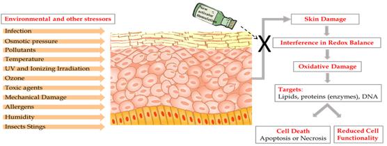
Caption: These are the consequences of skin exposure to stressors. Credit: Maya Ben-Yehuda Greenwald
Here’s a link to and a citation for the paper,
Skin Redox Balance Maintenance: The Need for an Nrf2-Activator Delivery System by Maya Ben-Yehuda Greenwald, Shmuel Ben-Sasson, Havazelet Bianco-Peled, and Ron Kohen. Cosmetics 2016, 3(1), 1; doi:10.3390/cosmetics3010001 Published: 15 January 2016
This paper appears to be open access.
![Figure 1. A brief chronology of the evolution of e-skin. We emphasize several science fictional events in popular culture that inspired subsequent critical technological advancements in the development of e-skin. Images reproduced with permission: “micro-structured pressure sensor,”[18] “stretchable OLEDs,”[20b] “stretchable OPVs,”[21a] “stretchable, transparent e-skin,”[22] “macroscale nanowire e-skin,”[23a] “rechargeable, stretchable batteries,”[137] “interlocked e-skin.”[25] Copyright, respectively, 2010, 2009, 2012, 2005, 2010, 2013, 2012. Macmillan Publishers Ltd. “Flexible, active-matrix e-skin” image reproduced with permission.[26a] Copyright, 2004. National Academy of Sciences USA. “Epidermal electronics” image reproduced with permission.[390a] Copyright, American Association for the Advancement of Science. “Stretchable batteries” image reproduced with permission.[27] “Infrared e-skin” image reproduced with permission.[8b] Copyright 2001, IEEE. “Anthropomorphic cybernetic hand” image reproduced with permission.[426] Copyright 2006, IEEE. [downloaded from http://onlinelibrary.wiley.com.proxy.lib.sfu.ca/doi/10.1002/adma.201302240/full]](http://www.frogheart.ca/wp-content/uploads/2013/11/e-skinTimeline.png)
![Chip containing U.S. and Israeli Declarations of Independence, on Jerusalem stone (downloaded from http://www.ats.org/site/News2?page=NewsArticle&id=7807&news_iv_ctrl=1161]](http://www.frogheart.ca/wp-content/uploads/2013/03/TechnionDeclOfIndep.jpg)