Tag Archives: Teri W. Odom

Colo(u)r-changing nanolaser inspired by chameleons

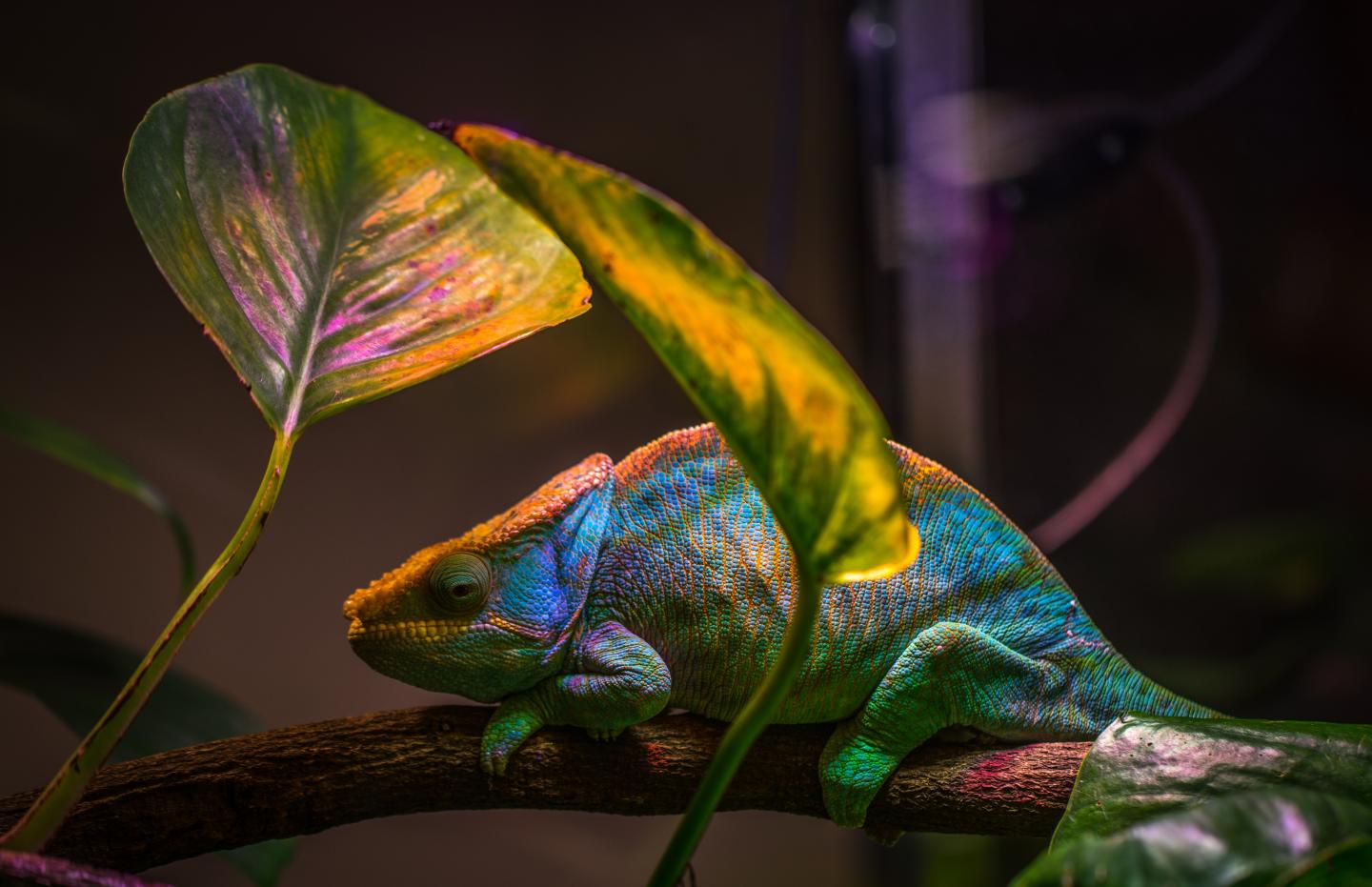
Caption: Novel nanolaser leverages the same color-changing mechanism that a chameleon uses to camouflage its skin. Credit: Egor Kamelev Courtesy: Northwestern University

I wish there was some detail included about how those colo(u)rs were achieved in that photograph. Strangely, Northwestern University (Chicago, Illinois, US) is more interested in describing the technology that chameleons have inspired. A June 20, 2018 news item on ScienceDaily announces the research,

As a chameleon shifts its color from turquoise to pink to orange to green, nature’s design principles are at play. Complex nano-mechanics are quietly and effortlessly working to camouflage the lizard’s skin to match its environment.

Inspired by nature, a Northwestern University team has developed a novel nanolaser that changes colors using the same mechanism as chameleons. The work could open the door for advances in flexible optical displays in smartphones and televisions, wearable photonic devices and ultra-sensitive sensors that measure strain.

A June 20, 2018 Northwestern University news release (also on EurekAlert) by Amanda Morris, which originated the news item, expands on the theme,

“Chameleons can easily change their colors by controlling the spacing among the nanocrystals on their skin, which determines the color we observe,” said Teri W. Odom, Charles E. and Emma H. Morrison Professor of Chemistry in Northwestern’s Weinberg College of Arts and Sciences. “This coloring based on surface structure is chemically stable and robust.”

The research was published online yesterday [June 19, 2018] in the journal Nano Letters. Odom, who is the associate director of Northwestern’s International Institute of Nanotechnology, and George C. Schatz, Charles E. and Emma H. Morrison Professor of Chemistry in Weinberg, served as the paper’s co-corresponding authors.

The same way a chameleon controls the spacing of nanocrystals on its skin, the Northwestern team’s laser exploits periodic arrays of metal nanoparticles on a stretchable, polymer matrix. As the matrix either stretches to pull the nanoparticles farther apart or contracts to push them closer together, the wavelength emitted from the laser changes wavelength, which also changes its color.

“Hence, by stretching and releasing the elastomer substrate, we could select the emission color at will,” Odom said.

The resulting laser is robust, tunable, reversible and has a high sensitivity to strain. These properties are critical for applications in responsive optical displays, on-chip photonic circuits and multiplexed optical communication.

Here’s a link to and a citation for the paper,

Stretchable Nanolasing from Hybrid Quadrupole Plasmons by Danqing Wang, Marc R. Bourgeois, Won-Kyu Lee, Ran Li, Dhara Trivedi, Michael P. Knudson, Weijia Wang, George C. Schatz, and Teri W. Odom. Nano Lett., Article ASAP DOI: 10.1021/acs.nanolett.8b01774 Publication Date (Web): June 18, 2018

Copyright © 2018 American Chemical Society

This paper is behind a paywall.

Liquid nanolaser: the first one

According to an April 24, 2015 news item on Nanowerk, there has been a big discovery at Northwestern University (located in Chicago, Illinois, US),

Northwestern University scientists have developed the first liquid nanoscale laser. And it’s tunable in real time, meaning you can quickly and simply produce different colors, a unique and useful feature. The laser technology could lead to practical applications, such as a new form of a “lab on a chip” for medical diagnostics.

To understand the concept, imagine a laser pointer whose color can be changed simply by changing the liquid inside it, instead of needing a different laser pointer for every desired color.

In addition to changing color in real time, the liquid nanolaser has additional advantages over other nanolasers: it is simple to make, inexpensive to produce and operates at room temperature.

An April 24, 2015 Northwestern University news release by Megan Fellman (also on EurekAlert), which originated the news item, offers a little history buttressed by some technical details (Note: Links have been removed),

Nanoscopic lasers — first demonstrated in 2009 — are only found in research labs today. They are, however, of great interest for advances in technology and for military applications.

“Our study allows us to think about new laser designs and what could be possible if they could actually be made,” said Teri W. Odom, who led the research. “My lab likes to go after new materials, new structures and new ways of putting them together to achieve things not yet imagined. We believe this work represents a conceptual and practical engineering advance for on-demand, reversible control of light from nanoscopic sources.”

The liquid nanolaser in this study is not a laser pointer but a laser device on a chip, Odom explained. The laser’s color can be changed in real time when the liquid dye in the microfluidic channel above the laser’s cavity is changed.

The laser’s cavity is made up of an array of reflective gold nanoparticles, where the light is concentrated around each nanoparticle and then amplified. (In contrast to conventional laser cavities, no mirrors are required for the light to bounce back and forth.) Notably, as the laser color is tuned, the nanoparticle cavity stays fixed and does not change; only the liquid gain around the nanoparticles changes.

The main advantages of very small lasers are:

• They can be used as on-chip light sources for optoelectronic integrated circuits;

• They can be used in optical data storage and lithography;

• They can operate reliably at one wavelength; and

• They should be able to operate much faster than conventional lasers because they are made from metals.

Some technical background

Plasmon lasers are promising nanoscale coherent sources of optical fields because they support ultra-small sizes and show ultra-fast dynamics. Although plasmon lasers have been demonstrated at different spectral ranges, from the ultraviolet to near-infrared, a systematic approach to manipulate the lasing emission wavelength in real time has not been possible.

The main limitation is that only solid gain materials have been used in previous work on plasmon nanolasers; hence, fixed wavelengths were shown because solid materials cannot easily be modified. Odom’s research team has found a way to integrate liquid gain materials with gold nanoparticle arrays to achieve nanoscale plasmon lasing that can be tuned dynamical, reversibly and in real time.

The use of liquid gain materials has two significant benefits:

• The organic dye molecules can be readily dissolved in solvents with different refractive indices. Thus, the dielectric environment around the nanoparticle arrays can be tuned, which also tunes the lasing wavelength.

• The liquid form of gain materials enables the fluid to be manipulated within a microfluidic channel. Thus, dynamic tuning of the lasing emission is possible simply by flowing liquid with different refractive indices. Moreover, as an added benefit of the liquid environment, the lasing-on-chip devices can show long-term stability because the gain molecules can be constantly refreshed.

These nanoscale lasers can be mass-produced with emission wavelengths over the entire gain bandwidth of the dye. Thus, the same fixed nanocavity structure (the same gold nanoparticle array) can exhibit lasing wavelengths that can be tuned over 50 nanometers, from 860 to 910 nanometers, simply by changing the solvent the dye is dissolved in.

Here’s a link to and a citation for the paper,

Real-time tunable lasing from plasmonic nanocavity arrays by Ankun Yang, Thang B. Hoang, Montacer Dridi, Claire Deeb, Maiken H. Mikkelsen, George C. Schatz, & Teri W. Odom. Nature Communications 6, Article number: 6939 doi:10.1038/ncomms7939 Published 20 April 2015

This paper is open access.

Shrinky Dinks* instrumental for new nanowires technique

Shrinky Dinks, a material used for children’s arts and crafts projects, has proved instrumental for developing a new technique to close the gap between nanowires. From a July 1, 2014 news item on Nanowerk (Note: A link has been removed),

How do you put a puzzle together when the pieces are too tiny to pick up? Shrink the distance between them.

Engineers at the University of Illinois at Urbana-Champaign are using Shrinky Dinks, plastic that shrinks under high heat, to close the gap between nanowires in an array to make them useful for high-performance electronics applications. The group published its technique in the journal Nano Letters (“Assembly and Densification of Nanowire Arrays via Shrinkage”).

A July 1, 2014 University of Illinois at Urbana-Champaign news release, which originated the news item, provides more details about the new technique,

Nanowires are extremely fast, efficient semiconductors, but to be useful for electronics applications, they need to be packed together in dense arrays. Researchers have struggled to find a way to put large numbers of nanowires together so that they are aligned in the same direction and only one layer thick.

“Chemists have already done a brilliant job in making nanowires exhibit very high performance. We just don’t have a way to put them into a material that we can handle,” said study leader SungWoo Nam, a professor of mechanical science and engineering at the U. of I. “With the shrinking approach, people can make nanowires and nanotubes using any method they like and use the shrinking action to compact them into a higher density.”

The researchers place the nanowires on the Shrinky Dinks plastic as they would for any other substrate, but then shrink it to bring the wires much closer together. This allows them to create very dense arrays of nanowires in a simple, flexible and very controllable way.

The shrinking method has the added bonus of bringing the nanowires into alignment as they increase in density. Nam’s group demonstrated how even wires more than 30 degrees off-kilter can be brought into perfect alignment with their neighbors after shrinking.

“There’s assembly happening at the same time as the density increases,” Nam said, “so even if the wires are assembled in a disoriented direction we can still use this approach.”

The plastic is clamped before baking so that it only shrinks in one direction, so that the wires pack together but do not buckle. Clamping in different places could direct the arrays into interesting formations, according to Nam. The researchers also can control how densely the wires pack by varying the length of time the plastic is heated. They also are exploring using lasers to precisely shrink the plastic in specific patterns.

Nam first had the idea for using Shrinky Dinks plastic to assemble nanomaterials after seeing a microfluidics device that used channels made of shrinking plastic. He realized that the high degree of shrinking and the low cost of plastic could have a huge impact on nanowire assembly and processing for applications.

“I’m interested in this concept of synthesizing new materials that are assembled from nanoscale building blocks,” Nam said. “You can create new functions. For example, experiments have shown that film made of packed nanowires has properties that differ quite a bit from a crystal thin film.”

One application the group is now exploring is a thin film solar cell, made of densely packed nanowires, that could harvest energy from light much more efficiently than traditional thin-film solar cells.

I have featured the Shrinky Dinks product and its use for nanoscale fabrication before in an Aug. 16, 2010 posting which featured this reply from the lead researcher for that project on nanopatterning,

ETA Aug.17.10: I also contacted Teri W. Odom, professor at Northwestern University about why they use Slinky Dinks in their work. She very kindly responded with this:

Part of what we are interested in is the development of low-cost nanofabrication tools that can create macroscale areas of nanoscale patterns in a single step. For a variety of reasons, this end-product is hard to obtain—even though we and others have chipped away at this problem for years.

As an example, to achieve smaller and smaller separations between patterns, either expensive, top-down serial tools (such as electron beam lithography or scanning probe techniques) or bottom-up assembly methods need to be used. However, the former cannot easily create large areas of patterns, and the latter cannot readily control the separations of patterns.

We needed a way to obtain nanopatterns separated by specific distances on-demand. Here is where the Shrinky Dinks material comes in. My student had read a paper (published in 2007 in Lab on a Chip) about how this material was used to make microscale patterns starting from a pattern printed using a laser printer. I imagine his thought was: if this material could be used for microscale patterns, why not for nanoscale ones? It would be cheap, and it’s easy to order.

So, we combined this substrate with our new molding method—solvent assisted nanoscale embossing (SANE)—and could now heat the material to shrink the spacing between patterns. And thus, in some sense, we made available to any lab some of the capabilities of the billion-dollar nanofabrication industry for less than one-hundred dollars.

Getting back to this latest use of Shrinky Dinks, here’s a link to and a citation for the ‘nanowires’ research paper,

Assembly and Densification of Nanowire Arrays via Shrinkage by Jaehoon Bang, Jonghyun Choi, Fan Xia, Sun Sang Kwon, Ali Ashraf, Won Il Park, and SungWoo Nam. Nano Lett., 2014, 14 (6), pp 3304–3308 DOI: 10.1021/nl500709p Publication Date (Web): May 16, 2014
Copyright © 2014 American Chemical Society

This paper is behind a paywall.

* ‘dinks’ in headline changed to ‘Dinks’ on July 2, 2014 at 1150 hours PDT.

Using Shrinky Dinks for SANE nanopatterning

I’m charmed. Scientists at a Northwestern University laboratory have taken to using a children’s arts and crafts product, Shrinky Dinks, for a new way to create large area nanoscale patterns on the cheap. First, something more about the Shrinky Dinks (from their website),

We are the Originators and Manufacturers of SHRINKY DINKS shrinkable plastics.

The very first SHRINKY DINKS were sold on October 17, 1973 at Brookfield Square Shopping Mall in Brookfield Wisconsin. Since that time there has been over 250 different Toy Activity and Craft Kits created and marketed.

SHRINKY DINKS SHRINK to approximately 1/3rd their original size and actually become 9 times thicker. Simply place the SHRINKY DINKS piece you created into a Home Oven or Toaster Oven for 2 magic minutes. Watch as your creation gets smaller and smaller.

It’s “MAGICAL” and it’s so quick and easy to do!

There’s also a video (sadly I can’t embed it here)  about the origins, some very simple science, and ideas on how to use Shrinky Dinks.

As for the scientists, there’s no word on how they decided to use this  product for their work (from the news item on physorg.com),

“Anyone needing access to large-area nanoscale patterns on the cheap could benefit from this method,” said Teri W. Odom, associate professor of chemistry and Dow Chemical Company Research Professor in the Weinberg College of Arts and Sciences. Odom led the research. “It is a simple, low-cost and high-throughput nanopatterning method that can be done in any laboratory.”

Details of the solvent-assisted nanoscale embossing (SANE) method are published by the journal Nano Letters. The work also will appear as the cover story of the journal’s February 2011 issue.

The method offers unprecedented opportunities to manipulate the electronic, photonic and magnetic properties of nanomaterials. It also easily controls a pattern’s size and symmetry and can be used to produce millions of copies of the pattern over a large area. Potential applications include devices that take advantage of nanoscale patterns, such as solar cells, high-density displays, computers and chemical and biological sensors.

“No other existing nanopatterning method can both prototype arbitrary patterns with small separations and reproduce them over six-inch wafers for less than $100,” Odom said.

ETA Aug. 17, 2010: I emailed the originator of Shrinky Dinks, Betty J. Morris asking her how she came up with the name for her product yesterday. Here is her very kind reply,

You were wondering how we came up with the name Shrinky Dinks…To be honest, we were trying to come up with a name that would describe the process…the pieces “shrink” and they become “small”… what are words that mean small…one of the words we came up with was “dinky”…we thought of Shrink Dinky…Shrink Dinkies…Shrinkie Dinkies but ultimately liked the sound of Shrinky Dinks…it was just trying out different words that we thought might be unique and worthy of getting a Trademark…our product has now been on the market 37 years…we have Shrinky Dinks Trademarks in 42 different countries and there have been over 250 different SD kits created and marketed over the years…who would have ever imagined such a success story… not me…that’s for sure!

The story reminds me of how one writes a poem, playing with words.  As Betty says it is a remarkable story and, for me, the science (nanopaterning)/kid’s play (Shrinky Dinks) connection is the best part.

ETA Aug.17.10: I also contacted Teri W. Odom, professor at Northwestern University about why they use Slinky Dinks in their work. She very kindly responded with this:

Part of what we are interested in is the development of low-cost nanofabrication tools that can create macroscale areas of nanoscale patterns in a single step. For a variety of reasons, this end-product is hard to obtain—even though we and others have chipped away at this problem for years.

As an example, to achieve smaller and smaller separations between patterns, either expensive, top-down serial tools (such as electron beam lithography or scanning probe techniques) or bottom-up assembly methods need to be used. However, the former cannot easily create large areas of patterns, and the latter cannot readily control the separations of patterns.

We needed a way to obtain nanopatterns separated by specific distances on-demand. Here is where the Shrinky Dinks material comes in. My student had read a paper (published in 2007 in Lab on a Chip) about how this material was used to make microscale patterns starting from a pattern printed using a laser printer. I imagine his thought was: if this material could be used for microscale patterns, why not for nanoscale ones? It would be cheap, and it’s easy to order.

So, we combined this substrate with our new molding method—solvent assisted nanoscale embossing (SANE)—and could now heat the material to shrink the spacing between patterns. And thus, in some sense, we made available to any lab some of the capabilities of the billion-dollar nanofabrication industry for less than one-hundred dollars.

There is something pleasing about using an everyday, inexpensive product for high end technology. Brava!

ETA Aug.23.10: Michael Berger has written an in depth article at Nanoterk on this type of nanofabrication which includes an interview with Teri Odom.