Tag Archives: Texas

Better RRAM memory devices in the short term

Given my recent spate of posts about computing and the future of the chip (list to follow at the end of this post), this Rice University [Texas, US] research suggests that some improvements to current memory devices might be coming to the market in the near future. From a July 12, 2014 news item on Azonano,

Rice University’s breakthrough silicon oxide technology for high-density, next-generation computer memory is one step closer to mass production, thanks to a refinement that will allow manufacturers to fabricate devices at room temperature with conventional production methods.

A July 10, 2014 Rice University news release, which originated the news item, provides more detail,

Tour and colleagues began work on their breakthrough RRAM technology more than five years ago. The basic concept behind resistive memory devices is the insertion of a dielectric material — one that won’t normally conduct electricity — between two wires. When a sufficiently high voltage is applied across the wires, a narrow conduction path can be formed through the dielectric material.

The presence or absence of these conduction pathways can be used to represent the binary 1s and 0s of digital data. Research with a number of dielectric materials over the past decade has shown that such conduction pathways can be formed, broken and reformed thousands of times, which means RRAM can be used as the basis of rewritable random-access memory.

RRAM is under development worldwide and expected to supplant flash memory technology in the marketplace within a few years because it is faster than flash and can pack far more information into less space. For example, manufacturers have announced plans for RRAM prototype chips that will be capable of storing about one terabyte of data on a device the size of a postage stamp — more than 50 times the data density of current flash memory technology.

The key ingredient of Rice’s RRAM is its dielectric component, silicon oxide. Silicon is the most abundant element on Earth and the basic ingredient in conventional microchips. Microelectronics fabrication technologies based on silicon are widespread and easily understood, but until the 2010 discovery of conductive filament pathways in silicon oxide in Tour’s lab, the material wasn’t considered an option for RRAM.

Since then, Tour’s team has raced to further develop its RRAM and even used it for exotic new devices like transparent flexible memory chips. At the same time, the researchers also conducted countless tests to compare the performance of silicon oxide memories with competing dielectric RRAM technologies.

“Our technology is the only one that satisfies every market requirement, both from a production and a performance standpoint, for nonvolatile memory,” Tour said. “It can be manufactured at room temperature, has an extremely low forming voltage, high on-off ratio, low power consumption, nine-bit capacity per cell, exceptional switching speeds and excellent cycling endurance.”

In the latest study, a team headed by lead author and Rice postdoctoral researcher Gunuk Wang showed that using a porous version of silicon oxide could dramatically improve Rice’s RRAM in several ways. First, the porous material reduced the forming voltage — the power needed to form conduction pathways — to less than two volts, a 13-fold improvement over the team’s previous best and a number that stacks up against competing RRAM technologies. In addition, the porous silicon oxide also allowed Tour’s team to eliminate the need for a “device edge structure.”

“That means we can take a sheet of porous silicon oxide and just drop down electrodes without having to fabricate edges,” Tour said. “When we made our initial announcement about silicon oxide in 2010, one of the first questions I got from industry was whether we could do this without fabricating edges. At the time we could not, but the change to porous silicon oxide finally allows us to do that.”

Wang said, “We also demonstrated that the porous silicon oxide material increased the endurance cycles more than 100 times as compared with previous nonporous silicon oxide memories. Finally, the porous silicon oxide material has a capacity of up to nine bits per cell that is highest number among oxide-based memories, and the multiple capacity is unaffected by high temperatures.”

Tour said the latest developments with porous silicon oxide — reduced forming voltage, elimination of need for edge fabrication, excellent endurance cycling and multi-bit capacity — are extremely appealing to memory companies.

“This is a major accomplishment, and we’ve already been approached by companies interested in licensing this new technology,” he said.

Here’s a link to and a citation for the paper,

Nanoporous Silicon Oxide Memory by Gunuk Wang, Yang Yang, Jae-Hwang Lee, Vera Abramova, Huilong Fei, Gedeng Ruan, Edwin L. Thomas, and James M. Tour. Nano Lett., Article ASAP DOI: 10.1021/nl501803s Publication Date (Web): July 3, 2014

Copyright © 2014 American Chemical Society

This paper is behind a paywall.

As for my recent spate of posts on computers and chips, there’s a July 11, 2014 posting about IBM, a 7nm chip, and much more; a July 9, 2014 posting about Intel and its 14nm low-power chip processing and plans for a 10nm chip; and, finally, a June 26, 2014 posting about HP Labs and its plans for memristive-based computing and their project dubbed ‘The Machine’.
Harvest water from desert air with carbon nanotube cups (competition for NBD Nano?)

It’s been a while since I’ve seen Pulickel Ajayan’s name in a Rice University (Texas) news release and I wonder if this is the beginning of a series. I’ve noticed that researchers often publish a series of papers within a few months and then become quiet for two or more years as they work in their labs to gather more information.

This time the research from Pulickel’s lab has focused on the use of carbon nanotubes to harvest water from desert air. From a June 12, 2014 news item on Azonano,

If you don’t want to die of thirst in the desert, be like the beetle. Or have a nanotube cup handy.

New research by scientists at Rice University demonstrated that forests of carbon nanotubes can be made to harvest water molecules from arid desert air and store them for future use.

The invention they call a “hygroscopic scaffold” is detailed in a new paper in the American Chemical Society journal Applied Materials and Interfaces.

Researchers in the lab of Rice materials scientist Pulickel Ajayan found a way to mimic the Stenocara beetle, which survives in the desert by stretching its wings to capture and drink water molecules from the early morning fog.

Here’s more about the research from a June 11, 2014 Rice University news release (by Mike Williams?), which originated the news item,

They modified carbon nanotube forests grown through a process created at Rice, giving the nanotubes a superhydrophobic (water-repelling) bottom and a hydrophilic (water loving) top. The forest attracts water molecules from the air and, because the sides are naturally hydrophobic, traps them inside.

“It doesn’t require any external energy, and it keeps water inside the forest,” said graduate student and first author Sehmus Ozden. “You can squeeze the forest to take the water out and use the material again.”

The forests grown via water-assisted chemical vapor deposition consist of nanotubes that measure only a few nanometers (billionths of a meter) across and about a centimeter long.

The Rice team led by Ozden deposited a superhydrophobic layer to the top of the forest and then removed the forest from its silicon base, flipped it and added a layer of hydrophilic polymer to the other side.

In tests, water molecules bonded to the hydrophilic top and penetrated the forest through capillary action and gravity. (Air inside the forest is compressed rather then expelled, the researchers assumed.) Once a little water bonds to the forest canopy, the effect multiplies as the molecules are drawn inside, spreading out over the nanotubes through van der Waals forces, hydrogen bonding and dipole interactions. The molecules then draw more water in.

The researchers tested several variants of their cup. With only the top hydrophilic layer, the forests fell apart when exposed to humid air because the untreated bottom lacked the polymer links that held the top together. With a hydrophilic top and bottom, the forest held together but water ran right through.

But with a hydrophobic bottom and hydrophilic top, the forest remained intact even after collecting 80 percent of its weight in water.

The amount of water vapor captured depends on the air’s humidity. An 8 milligram sample (with a 0.25-square-centimeter surface) pulled in 27.4 percent of its weight over 11 hours in dry air, and 80 percent over 13 hours in humid air. Further tests showed the forests significantly slowed evaporation of the trapped water.

If it becomes possible to grow nanotube forests on a large scale, the invention could become an efficient, effective water-collection device because it does not require an external energy source, the researchers said.

Ozden said the production of carbon nanotube arrays at a scale necessary to put the invention to practical use remains a bottleneck. “If it becomes possible to make large-scale nanotube forests, it will be a very easy material to make,” he said.

This is not the first time researchers have used the Stenocara beetle (also known as the Namib desert beetle) as inspiration for a water-harvesting material. In a Nov. 26, 2012 posting I traced the inspiration  back to 2001 while featuring the announcement of a new startup company,

… US startup company, NBD Nano, which aims to bring a self-filling water bottle based on Namib desert beetle to market,

NBD Nano, which consists of four recent university graduates and was formed in May [2012], looked at the Namib Desert beetle that lives in a region that gets about half an inch of rainfall per year.

Using a similar approach, the firm wants to cover the surface of a bottle with hydrophilic (water-attracting) and hydrophobic (water-repellent) materials.

The work is still in its early stages, but it is the latest example of researchers looking at nature to find inspiration for sustainable technology.

“It was important to apply [biomimicry] to our design and we have developed a proof of concept and [are] currently creating our first fully-functional prototype,” Miguel Galvez, a co-founder, told the BBC.

“We think our initial prototype will collect anywhere from half a litre of water to three litres per hour, depending on local environments.”

You can find out more about NBD Nano here although they don’t give many details about the material they’ve developed. Given that MIT (Massachusetts Institute of Technology) researchers published a  paper about a polymer-based material laced with silicon nanoparticles inspired by the Namib beetle in 2006 and that NBD Nano is based Massachusetts, I believe NBD Nano is attempting to commercialize the material or some variant developed at MIT.

Getting back to Rice University and carbon nanotubes, this is a different material attempting to achieve the same goal, harvesting water from desert air. Here’s a link to and a citation for the latest paper inspired by the Stenocara beetle (Namib beetle),

Anisotropically Functionalized Carbon Nanotube Array Based Hygroscopic Scaffolds by Sehmus Ozden, Liehui Ge , Tharangattu N. Narayanan , Amelia H. C. Hart , Hyunseung Yang , Srividya Sridhar , Robert Vajtai , and Pulickel M Ajayan. ACS Appl. Mater. Interfaces, DOI: 10.1021/am5022717 Publication Date (Web): June 4, 2014

Copyright © 2014 American Chemical Society

This paper is behind a paywall.

One final note, the research at MIT was funded by DARPA (US Defense Advanced Research Projects Agency). According to the news release the Rice University research held interest for similar agencies,

The U.S. Department of Defense and the U.S. Air Force Office of Scientific Research Multidisciplinary University Research Initiative supported the research.

Carbon capture with nanoporous material in the oilfields

Researchers at Rice University (Texas) have devised a new technique for carbon capture according to a June 3, 2014 news item on Nanowerk,

Rice University scientists have created an Earth-friendly way to separate carbon dioxide from natural gas at wellheads.

A porous material invented by the Rice lab of chemist James Tour sequesters carbon dioxide, a greenhouse gas, at ambient temperature with pressure provided by the wellhead and lets it go once the pressure is released. The material shows promise to replace more costly and energy-intensive processes.

A June 3, 2014 Rice University news release, which originated the news item, provides a general description of how carbon dioxide is currently removed during fossil fuel production and adds a few more details about the new technology,

Natural gas is the cleanest fossil fuel. Development of cost-effective means to separate carbon dioxide during the production process will improve this advantage over other fossil fuels and enable the economic production of gas resources with higher carbon dioxide content that would be too costly to recover using current carbon capture technologies, Tour said. Traditionally, carbon dioxide has been removed from natural gas to meet pipelines’ specifications.

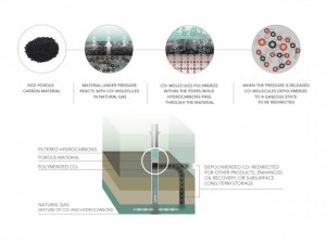
The Tour lab, with assistance from the National Institute of Standards and Technology (NIST), produced the patented material that pulls only carbon dioxide molecules from flowing natural gas and polymerizes them while under pressure naturally provided by the well.

When the pressure is released, the carbon dioxide spontaneously depolymerizes and frees the sorbent material to collect more.

All of this works in ambient temperatures, unlike current high-temperature capture technologies that use up a significant portion of the energy being produced.

The news release mentions current political/legislative actions in the US and the implications for the oil and gas industry while further describing the advantages of this new technique,

“If the oil and gas industry does not respond to concerns about carbon dioxide and other emissions, it could well face new regulations,” Tour said, noting the White House issued its latest National Climate Assessment last month [May 2014] and, this week [June 2, 2014], set new rules to cut carbon pollution from the nation’s power plants.

“Our technique allows one to specifically remove carbon dioxide at the source. It doesn’t have to be transported to a collection station to do the separation,” he said. “This will be especially effective offshore, where the footprint of traditional methods that involve scrubbing towers or membranes are too cumbersome.

“This will enable companies to pump carbon dioxide directly back downhole, where it’s been for millions of years, or use it for enhanced oil recovery to further the release of oil and natural gas. Or they can package and sell it for other industrial applications,” he said.

This is an epic (Note to writer: well done) news release as only now is there a technical explanation,

The Rice material, a nanoporous solid of carbon with nitrogen or sulfur, is inexpensive and simple to produce compared with the liquid amine-based scrubbers used now, Tour said. “Amines are corrosive and hard on equipment,” he said. “They do capture carbon dioxide, but they need to be heated to about 140 degrees Celsius to release it for permanent storage. That’s a terrible waste of energy.”

Rice graduate student Chih-Chau Hwang, lead author of the paper, first tried to combine amines with porous carbon. “But I still needed to heat it to break the covalent bonds between the amine and carbon dioxide molecules,” he said. Hwang also considered metal oxide frameworks that trap carbon dioxide molecules, but they had the unfortunate side effect of capturing the desired methane as well and they are far too expensive to make for this application.

The porous carbon powder he settled on has massive surface area and turns the neat trick of converting gaseous carbon dioxide into solid polymer chains that nestle in the pores.

“Nobody’s ever seen a mechanism like this,” Tour said. “You’ve got to have that nucleophile (the sulfur or nitrogen atoms) to start the polymerization reaction. This would never work on simple activated carbon; the key is that the polymer forms and provides continuous selectivity for carbon dioxide.”

Methane, ethane and propane molecules that make up natural gas may try to stick to the carbon, but the growing polymer chains simply push them off, he said.

The researchers treated their carbon source with potassium hydroxide at 600 degrees Celsius to produce the powders with either sulfur or nitrogen atoms evenly distributed through the resulting porous material. The sulfur-infused powder performed best, absorbing 82 percent of its weight in carbon dioxide. The nitrogen-infused powder was nearly as good and improved with further processing.

Tour said the material did not degrade over many cycles, “and my guess is we won’t see any. After heating it to 600 degrees C for the one-step synthesis from inexpensive industrial polymers, the final carbon material has a surface area of 2,500 square meters per gram, and it is enormously robust and extremely stable.”

Apache Corp., a Houston-based oil and gas exploration and production company, funded the research at Rice and licensed the technology. Tour expected it will take time and more work on manufacturing and engineering aspects to commercialize.

Here’s a link to and a citation for the paper,

Capturing carbon dioxide as a polymer from natural gas by Chih-Chau Hwang, Josiah J. Tour, Carter Kittrell, Laura Espinal, Lawrence B. Alemany, & James M. Tour. Nature Communications 5, Article number: 3961 doi:10.1038/ncomms4961 Published 03 June 2014

This paper is behind a paywall.

The researchers have made an illustration of the material available,

 Illustration by Tanyia Johnson/Rice University

Illustration by Tanyia Johnson/Rice University

This morning, Azonano posted a June 6, 2014 news item about a patent for carbon capture,

CO2 Solutions Inc. ( the “Corporation”), an innovator in the field of enzyme-enabled carbon capture technology, today announced it has received a Notice of Allowance from the U.S. Patent and Trademark Office for its patent application No. 13/264,294 entitled Process for CO2 Capture Using Micro-Particles Comprising Biocatalysts.

One might almost think these announcements were timed to coincide with the US White House’s moves.

As for CO2 Solutions, this company is located in Québec, Canada.  You can find out more about the company here (you may want to click on the English language button).

Tracking gas, oil, and, possibly, water in wells

A Feb. 24, 2014 Rice University news release (also on EurekAlert) and on Azonano as a Feb. 25, 2014 news item) describes a technique tracks which wells are producing oil or gas in fracking operations,

A tabletop device invented at Rice University can tell how efficiently a nanoparticle would travel through a well and may provide a wealth of information for oil and gas producers.

The device gathers data on how tracers – microscopic particles that can be pumped into and recovered from wells – move through deep rock formations that have been opened by hydraulic fracturing [fracking].

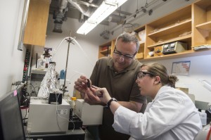
Here’s an image of two Rice scientists playing around with a prototype of their tabletop device,

Rice University chemist Andrew Barron and graduate student Brittany Oliva-Chatelain investigate the prototype of a device that allows for rapid testing of nanotracers for the evaluation of wells subject to hydraulic fracturing. (Credit: Jeff Fitlow/Rice University)

Rice University chemist Andrew Barron and graduate student Brittany Oliva-Chatelain investigate the prototype of a device that allows for rapid testing of nanotracers for the evaluation of wells subject to hydraulic fracturing. (Credit: Jeff Fitlow/Rice University)

The news release goes on to describe the fracking process and explain why the companies don’t know which well is actually producing (Note: Links have been removed),

Drilling companies use fracturing to pump oil and gas from previously unreachable reservoirs. Fluids are pumped into a wellbore under high pressure to fracture rocks, and materials called “proppants,” like sand or ceramic, hold the fractures open. “They’re basically making a crack in the rock and filling it with little beads,” said Rice chemist Andrew Barron, whose lab produced the device detailed in the Royal Society of Chemistry journal Environmental Science Processes and Impacts.

But the companies struggle to know which insertion wells — where fluids are pumped in — are connected to the production wells where oil and gas are pumped out. “They may be pumping down three wells and producing from six, but they have very little idea of which well is connected to which,” he said.

Tracer or sensor particles added to fracturing fluids help solve that problem, but there’s plenty of room for optimization, especially in minimizing the volume of nanoparticles used now, he said. “Ideally, we would take a very small amount of a particle that does not interact with proppant, rock or the gunk that’s been pumped downhole, inject it in one well and collect it at the production well. The time it takes to go from one to the other will tell you about the connectivity underground.”

Barron explained the proppant itself accounts for most of the surface area the nanoparticles encounter, so it’s important to tune the tracers to the type of proppant used.

He said the industry lacks a uniform method to test and optimize custom-designed nanoparticles for particular formations and fluids. The ultimate goal  is to optimize the particles so they don’t clump together or stick to the rock or proppant and can be reliably identified when they exit the production well.

Here’s how the tracers work (from the news release),

The automated device by Barron, Rice alumnus Samuel Maguire-Boyle and their colleagues allows them to run nanotracers through a small model of a geological formation and quickly analyze what comes out the other side.

The device sends a tiny amount of silver nanoparticle tracers in rapid pulses through a solid column, simulating the much longer path the particles would travel in a well. That gives the researchers an accurate look at both how sticky and how robust the particles are.

“We chose silver nanoparticles for their plasmon resonance,” Barron said. “They’re very easy to see (with a spectroscope) making for high-quality data.” He said silver nanoparticles would be impractical in a real well, but because they’re easy to modify with other useful chemicals, they are good models for custom nanoparticles.

“The process is simple enough that our undergraduates make different nanoparticles and very quickly test them to find out how they behave,” Barron said.

The method also shows promise for tracking water from source to destination, which could be valuable for government agencies that want to understand how aquifers are linked or want to trace the flow of elements like pollutants in a water supply, he said.

Barron said the Rice lab won’t oversee production of the test rig, but it doesn’t have to. “We just published the paper, but if companies want to make their own, it includes the instructions. The supplementary material is basically a manual for how to do this,” he said.

You can find the paper with this link and/or citation,

Automated method for determining the flow of surface functionalized nanoparticles through a hydraulically fractured mineral formation using plasmonic silver nanoparticles by Samuel J. Maguire-Boyle, David J. Garner, Jessica E. Heimann, Lucy Gao, Alvin W. Orbaek, and Andrew R. Barron. Environ. Sci.: Processes Impacts, 2014,16, 220-231 DOI: 10.1039/C3EM00718A First published online 07 Jan 2014

This paper has been published in one of the Royal Society’s open access journals.

My final note, one of my more recent posts about fracking highlights some research that was taking place in Texas (Rice University’s home state) at Texas A&M University, see my July 29, 2013 posting.

Control the chirality, control your carbon nanotube

A Feb. 18, 2014 news item on ScienceDaily features a story not about a breakthrough but about a discovery that* could lead to one,

A single-walled carbon nanotube grows from the round cap down, so it’s logical to think the cap’s formation determines what follows. But according to researchers at Rice University, that’s not entirely so.

Theoretical physicist Boris Yakobson and his Rice colleagues found through exhaustive analysis that those who wish to control the chirality of nanotubes — the characteristic that determines their electrical properties — would be wise to look at other aspects of their growth.

The scientists have provided this image to illustrate chirality (‘twisting’) in carbon nanotubes,

Carbon nanotube caps are forced into shape by six pentagons among the array of hexagons in the single-atom-thick tube. Rice University researchers took a census of thousands of possible caps and found the energies dedicated to their formation have no bearing on the tube's ultimate chirality. Credit: Evgeni Penev/Rice University

Carbon nanotube caps are forced into shape by six pentagons among the array of hexagons in the single-atom-thick tube. Rice University researchers took a census of thousands of possible caps and found the energies dedicated to their formation have no bearing on the tube’s ultimate chirality.
Credit: Evgeni Penev/Rice University

The Feb. 17, 2014 Rice University news release (also on EurekAlert), which originated the news item, describe the process the scientists used to research chirality in carbon nanotubes,

To get a clear picture of how caps are related to nanotube chirality, the Rice group embarked upon a detailed, two-year census of the 4,500 possible cap formations for nanotubes of just two diameters, 0.8 and 1 nanometer, across 21 chiralities.

The cap of every nanotube has six pentagons – none of which may touch each other — among an array of hexagons, Penev said. They pull the cap and force it to curve, but their positions are not always the same from cap to cap.

But because a given chirality can have hundreds of possible caps, the determining factor for chirality must lie elsewhere, the researchers found. “The contribution of the cap is the elastic curvature energy, and then you just forget it,” Penev said.

“There are different factors that may be in play,” Yakobson said. “One is the energy portion dictated by the catalyst; another one may be the energy of the caps per se. So to get the big picture, we address the energy of the caps and basically rule it out as a factor in determining chirality.”

A nanotube is an atom-thick sheet of carbon atoms arranged in hexagons and rolled into a tube. Chirality refers to the hexagons’ orientation, and that angle controls how well the nanotube will conduct electricity.

A perfect conducting metallic nanotube would have the atoms arranged in “armchairs,” so-called because cutting the nanotube in half would make the top look like a series of wells with atoms for armrests. Turn the hexagons 30 degrees, though, will make a semiconducting “zigzag” nanotube.  Nanotubes can be one or the other, or the chiral angle can be anything in between, with a shifting range of electrical properties.

Getting control of these properties has been a struggle. Ideally, scientists could grow the specific kinds of nanotubes they need for an application, but in reality, they grow as a random assortment that must then be separated with a centrifuge or by other means.

Yakobson suspects the answer lies in tuning the interaction between the catalyst and the nanotube edge. “This study showed the energy involved in configuring the cap is reasonably flat,” he said. “That’s important to know because it allows us to continue to work on other factors.

Here’s a  link to and a citation for the paper,

Extensive Energy Landscape Sampling of Nanotube End-Caps Reveals No Chiral-Angle Bias for Their Nucleation by Evgeni S. Penev, Vasilii I. Artyukhov, and Boris I. Yakobson. ACS Nano, Article ASAP DOI: 10.1021/nn406462e Publication Date (Web): January 23, 2014
Copyright © 2014 American Chemical Society

This article is behind a paywall.

One final comment, it took these scientists two years of painstaking work to establish that caps are not the determining factor for chirality. It’s this type of story I find as fascinating, if not more so, as the big breakthroughs because it illustrates the  extraordinary drive it takes to extract even the smallest piece of information. I wish more attention was given to these incremental efforts.

* March 7, 2014 changed ‘while’ to ‘that’.

Quadruple the amount of electrical current by using carbon nanotube-based fibers

The announcement from Rice University was written in an interesting fashion. The good news is that you can quadruple the amount of electrical current being carried by substituting copper with carbon nanotube-based fibers. Unfortunately, expectations are set for a much higher rate before the good news is revealed in this Feb.  14, 2013 news item on ScienceDaily,

On a pound-per-pound basis, carbon nanotube-based fibers invented at Rice University have greater capacity to carry electrical current than copper cables of the same mass, according to new research.

While individual nanotubes are capable of transmitting nearly 1,000 times more current than copper, the same tubes coalesced into a fiber using other technologies fail long before reaching that capacity.

But a series of tests at Rice showed the wet-spun carbon nanotube fiber still handily beat copper, carrying up to four times as much current as a copper wire of the same mass. [emphasis mine]

That, said the researchers, makes nanotube-based cables an ideal platform for lightweight power transmission in systems where weight is a significant factor, like aerospace applications.

The Feb. 13, 2014 Rice University news release (dated as Feb. 14, 2014 on EurekAlert), which originated the news item, provides context for this discovery (Note: Links have been removed),

The analysis led by Rice professors Junichiro Kono and Matteo Pasquali appeared online this week [week of Feb. 10 – 14, 2014] in the journal Advanced Functional Materials. Just a year ago [2013] the journal Science reported that Pasquali’s lab, in collaboration with scientists at the Dutch firm Teijin Aramid, created a very strong conductive fiber out of carbon nanotubes.

Present-day transmission cables made of copper or aluminum are heavy because their low tensile strength requires steel-core reinforcement.

Scientists working with nanoscale materials have long thought there’s a better way to move electricity from here to there. Certain types of carbon nanotubes can carry far more electricity than copper. The ideal cable would be made of long metallic “armchair” nanotubes that would transmit current over great distances with negligible loss, but such a cable is not feasible because it’s not yet possible to manufacture pure armchairs in bulk, Pasquali said.

I have a couple of notes (1) the 2013 work on ‘armchair’ carbon nanotubes was featured here in a Feb. 6, 2013 posting and (2) Teijin Aramid is located in the Netherlands while its parent company, Teijin, is located in Japan (you can find more about Teijin in this Wikipedia essay).

Getting back to this latest work from Rice (from the news release),

In the meantime, the Pasquali lab has created a method to spin fiber from a mix of nanotube types that still outperforms copper. The cable developed by Pasquali and Teijin Aramid is strong and flexible even though at 20 microns wide, it’s thinner than a human hair.

Pasquali turned to Kono and his colleagues, including lead author Xuan Wang, a postdoctoral researcher at Rice, to quantify the fiber’s capabilities.

Pasquali said there has been a disconnect between electrical engineers who study the current carrying capacity of conductors and materials scientists working on carbon nanotubes. “That has generated some confusion in the literature over the right comparisons to make,” he said. “Jun and Xuan really got to the bottom of how to do these measurements well and compare apples to apples.”

The researchers analyzed the fiber’s “current carrying capacity” (CCC), or ampacity, with a custom rig that allowed them to test it alongside metal cables of the same diameter. The cables were tested while they were suspended in the open air, in a vacuum and in nitrogen or argon environments.

Electric cables heat up because of resistance. When the current load exceeds the cable’s safe capacity, they get too hot and break. The researchers found nanotube fibers exposed to nitrogen performed best, followed by argon and open air, all of which were able to cool through convection. The same nanotube fibers in a vacuum could only cool by radiation and had the lowest CCC.

“The outcome is that these fibers have the highest CCC ever reported for any carbon-based fibers,” Kono said. “Copper still has better resistivity by an order of magnitude, but we have the advantage that carbon fiber is light. So if you divide the CCC by the mass, we win.”

Kono plans to further investigate and explore the fiber’s multifunctional aspects, including flexible optoelectronic device applications.

Pasquali suggested the thread-like fibers are light enough to deliver power to aerial vehicles. “Suppose you want to power an unmanned aerial vehicle from the ground,” he mused. “You could make it like a kite, with power supplied by our fibers. I wish Ben Franklin were here to see that!”

Pasquali and his team’s latest research can be found here,

High-Ampacity Power Cables of Tightly-Packed and Aligned Carbon Nanotubes by Xuan Wang, Natnael Behabtu, Colin C. Young, Dmitri E. Tsentalovich, Matteo Pasqua, & Junichiro Kono. Advanced Functional Materials, Article first published online: 13 FEB 2014 DOI: 10.1002/adfm.201303865

© 2014 WILEY-VCH Verlag GmbH & Co. KGaA, Weinheim

This study is behind a paywall.

Diamane—a no pressure road map

Russian and US researchers have produced a road map for creating ‘diamane’, according to a Feb. 3, 2014  Rice University (Texas) news release (available on EurekAlert and also as a Feb. 4, 2014 news item on Azonano),

Perfect sheets of diamond a few atoms thick appear to be possible even without the big squeeze that makes natural gems.

Scientists have speculated about it and a few labs have even seen signs of what they call diamane, an extremely thin film of diamond that has all of diamond’s superior semiconducting and thermal properties.

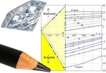
Now researchers at Rice University and in Russia have calculated a “phase diagram” for the creation of diamane. The diagram is a road map. It lays out the conditions – temperature, pressure and other factors – that would be necessary to turn stacked sheets of graphene into a flawless diamond lattice.

In the process, the researchers determined diamane could be made completely chemically, with no pressure at all, under some circumstances.

The news release provides more into the researchers’ theories and road map,

“Diamanes have a wide potential range of application,” Sorokin [Pavel Sorokin, a former postdoctoral associate at Rice and now a senior researcher at the Technological Institute for Superhard and Novel Carbon Materials in Moscow] said. “They can be applied as very thin, dielectric hard films in nanocapacitors or mechanically stiff, nanothick elements in nanoelectronics. Also, diamanes have potential for application in nano-optics.

“The possibility of obtaining such a quasi-two-dimensional object is intriguing, but available experimental data prevents the expectation of its fabrication using traditional methods. However, the ‘bottom-up’ approach proposed by Richard Feynman allows the fabrication of diamanes from smaller objects, such as graphene.”

The researchers built computer models to simulate the forces applied by every atom involved in the process. That includes the graphene, the single-atom-thick form of carbon and one of the strongest substances in the universe, as well as the hydrogen (or, alternately, a halogen) that promotes the reaction.

Conditions, they learned, need to be just right for a short stack of graphene pancakes to collapse into a diamond matrix – or vice versa – via chemistry.

“A phase diagram shows you which phase dominates the ground state for each pressure and temperature,” Yakobson [Rice theoretical physicist Boris Yakobson] said. “In the case of diamane, the diagram is unusual because the result also depends on thickness, the number of layers of graphene. So we have a new parameter.”

Hydrogen isn’t the only possible catalyst, he said, but it’s the one they used in their calculations. “When the hydrogen attacks, it takes one electron from a carbon atom in graphene. As a result, a bond is broken and another electron is left hanging on the other side of the graphene layer. It’s now free to connect to a carbon atom on the adjacent sheet with little or no pressure.

“If you have several layers, you get a domino effect, where hydrogen starts a reaction on top and it propagates through the bonded carbon system,” he said. “Once it zips all the way through, the phase transition is complete and the crystal structure is that of diamond.”

Yakobson said the paper doesn’t cover a possible deal-breaker. “The conversion from one phase to another starts from a small seed, a nucleation site, and in this process there’s always what is called a nucleation barrier. We don’t calculate that here.” He said carbon normally prefers to be graphite (the bulk form of carbon used as pencil lead) rather than diamond, but a high nucleation barrier prevents diamond from making the transition.

“Thermodynamically, an existing diamond should become graphite, but it doesn’t happen for exactly this reason,” Yakobson said. “So sometimes it’s a good thing. But if we want to make flat diamond, we need to find ways to circumvent this barrier.”

He said the manufacture of synthetic diamond, which was first reliably made in the 1950s, requires very high pressures of about 725,000 pounds per square inch. Manufactured diamonds are used in hardened tools for cutting, as abrasives and even as high-quality gemstones grown via techniques that simulate the temperatures and pressures found deep in Earth, where natural diamond is forged.

Diamond films are also routinely made via chemical vapor deposition, “but they’re always very poor quality because they’re polycrystalline,” Yakobson said. “For mechanical purposes, like very expensive sandpaper, they’re perfect. But for electronics, you would need high quality for it to serve as a wide-band gap semiconductor.”

This image illustrates the conditions necessary to create diamane,

The phase diagram developed by scientists at Rice University and in Moscow describes the conditions necessary for the chemical creation of thin films of diamond from stacks of single-atomic-layer graphene. (Credit: Pavel Sorokin/Technological Institute for Superhard and Novel Carbon Materials)

The phase diagram developed by scientists at Rice University and in Moscow describes the conditions necessary for the chemical creation of thin films of diamond from stacks of single-atomic-layer graphene. (Credit: Pavel Sorokin/Technological Institute for Superhard and Novel Carbon Materials)

Here’s a link to and a citation for the researchers’ paper,

Phase Diagram of Quasi-Two-Dimensional Carbon, From Graphene to Diamond by Alexander G. Kvashnin, Leonid A. Chernozatonskii, Boris I. Yakobson, and Pavel B. Sorokin. Nano Lett., Article ASAP DOI: 10.1021/nl403938g Publication Date (Web): January 17, 2014
Copyright © 2014 American Chemical Society

This paper is behind a paywall.

Université de Montréal (Canada) collaborates with University of Houston (US) for a new theory and better solar cells

Solar cell efficiency is not good as researchers from  l’Université de Montréal (UdeM, located in Quebec, Canada) and the University of Houston (UH, located Texas, US) note in a Jan. 29, 2014 joint UH/UdeM news release written by Lisa Merkl (UH) on EurekAlert,

“Scientists don’t fully understand what is going on inside the materials that make up solar cells. We were trying to get at the fundamental photochemistry or photophysics that describes how these cells work,” Bittner said [Eric Bittner, a John and Rebecca Moores Professor of Chemistry and Physics in UH’s College of Natural Sciences and Mathematics,].

Solar cells are made out of organic semiconductors – typically blends of materials. However, solar cells made of these materials have about 3 percent efficiency. Bittner added that the newer materials, the fullerene/polymer blends, only reach about 10 percent efficiency.

“There is a theoretical limit for the efficiency of the ideal solar cell – the Shockley-Queisser limit. The theory we published describes how we might be able to get above this theoretical limit by taking advantage of quantum mechanical effects,” Bittner said. “By understanding these effects and making use of them in the design of a solar cell, we believe you can improve efficiency.”

Silva [Carlos Silva, an associate professor at the Université de Montréal and Canada Research Chair in Organic Semiconductor Materials] added, “In polymeric semiconductors, where plastics form the active layer of solar cells, the electronic structure of the material is intimately correlated with the vibrational motion within the polymer chain. Quantum-mechanical effects due to such vibrational-electron coupling give rise to a plethora of interesting physical processes that can be controlled to optimize solar cell efficiencies by designing materials that best exploit them.”

Unfortunately, there’s no more information about this model other than this (from the news release),

“Our theoretical model accomplishes things that you can’t get from a molecular model,” he [Bittner] said. “It is mostly a mathematical model that allows us to look at a much larger system with thousands of molecules. You can’t do ordinary quantum chemistry calculations on a system of that size.”

The calculations have prompted a series of new experiments by Silva’s group to probe the outcomes predicted by their model.

Bittner and Silva’s next steps involve collaborations with researchers who are experts in making the polymers and fabricating solar cells.

Here’s a link to and a citation for the paper,

Noise-induced quantum coherence drives photo-carrier generation dynamics at polymeric semiconductor heterojunctions by Eric R. Bittner & Carlos Silva. Nature Communications 5, Article number: 3119 doi:10.1038/ncomms4119 Published 29 January 2014

This article is behind a paywall although you can get a free preview via ReadCube Access.

Lab tests show silver nanoparticles in cream blocks HIV entry for up to 72 hours

Since at least 2005 (the article reference will be given later in this posting), researchers have been aware that silver nanoparticles can block the HIV virus from entering a cell. The latest work in this area has resulted in a vaginal cream laced with silver nanoparticles according to a Jan. 28, 2014 news item on ScienceDaily,

Lara Villegas [Humberto Lara Villegas, specialist in nanoparticles and virology from the University of Monterrey, Mexico (UDEM)] explained that HIV makes its entry to immune cells (CD4) of the organism with the aid of a protein known as GP120, which allows the virus adherence to the cells. This same principle is used by silver nanoparticles to attach themselves to this protein and block it, turning the virus inactive.

The Mexican researcher informed that the cream has been tested in samples of human tissue and has proven the efficiency of silver nanoparticles to avoid the transmission of the virus through cervical mucous membrane.

The Jan. 28, 2014 Investigación y Desarrollo news release (on the Alpha Gallileo website), which originated the news item, provides additional details from Lara Villegas’ perspective,

The researcher from UDEM, who has worked in Israel and The United States, assured that after applied, the cream starts to work in less than a minute, and has an effective protection of up to 72 hours.

Given that the function of this product is the inactivation of the virus, although this is a vaginal cream, will also protect the sexual partner.

“Normally – he highlighted-, the medication used against the virus act within the cell to avoid its replication. This is a very different case, given that the nanoparticle goes directly against the HIV and no longer allows its entry to the cell”.

So far, no toxicity of the silver nanoparticles has been reported, although he added that research is yet to be performed to evaluate the possible side effects of silver properties.

“Right now, I am certain that this microbicide is going to avoid the virus entering the organism, but I cannot yet assure that is totally harmless, because the clinical trials are a long and expensive process”, the researched added.

He exposed that the use of gels are usually accompanied by irritation, which favors the entry of the virus, which is why the cream was enriched with an anti-inflammatory effect.

Currently, with the obtained results, researchers will proceed to perform experimentation in mice that accept human cells, to later begin with human clinical trials.

He added that this cream could prevent the transmition of other sexually acquired virus like the Human Papilloma Virus (HPV). Likewise, he considered that silver nanoparticles could be used to combat bacteria transmitted the same way.

As promised here’s a citation for and a link to the 2005 paper; I haven’t found any references in my admittedly brief search for a paper about this latest work,,

Interaction of silver nanoparticles with HIV-1 by Jose Luis Elechiguerra, Justin L Burt, Jose R Morones, Alejandra Camacho-Bragado, Xiaoxia Gao, Humberto H Lara, and Miguel Jose Yacaman. Journal of Nanobiotechnology 2005, 3:6  doi:10.1186/1477-3155-3-6

This paper is open access.

Here’s  the Investigación y Desarrollo website which seems to act as a hub for research in Mexico. Note: You will need Spanish language skills to fully utilize this site.

Rice University (Texas) researchers ‘soften’ a buckyball (buckminster fullerene)

A Jan. 16, 2014 Rice University news release landed in my mailbox this morning and revealed that researchers have ‘detuned’ or softened the atomic bonks in a molecule known as a buckminster fullenere (aka, buckyball),

Rice University scientists have found they can control the bonds between atoms in a molecule.

The molecule in question is carbon-60, also known as the buckminsterfullerene and the buckyball, discovered at Rice in 1985. The scientists led by Rice physicists Yajing Li and Douglas Natelson found that it’s possible to soften the bonds between atoms by applying a voltage and running an electric current through a single buckyball.

“This doesn’t mean we’re going to be able to arbitrarily dial around the strength of materials or anything like that,” Natelson said. “This is a very specific case, and even here it was something of a surprise to see this going on.

“But in general, if we can manipulate the charge distribution on molecules, we can affect their vibrations. We can start thinking, in the future, about controlling things in a better way.”

The effect appears when a buckyball attaches to a gold surface in the optical nano antenna used to measure the effects of an electric current on intermolecular bonds through a technique called Raman spectroscopy.

Natelson’s group built the nano antenna a few years ago to trap small numbers of molecules in a nanoscale gap between gold electrodes. Once the molecules are in place, the researchers can chill them, heat them, blast them with energy from a laser or electric current and measure the effect through spectroscopy, which gathers information from the frequencies of light emitted by the object of interest.

With continuing refinement, the researchers found they could analyze molecular vibrations and the bonds between the atoms in the molecule. That ability led to this experiment, Natelson said.

Natelson compared the characteristic vibrational frequencies exhibited by the bonds to the way a guitar string vibrates at a specific frequency based on how tightly it’s wound. Loosen the string and the vibration diminishes and the tone drops.

The nano antenna is able to detect the “tone” of detuned vibrations between atoms through surface-enhanced Raman spectroscopy (SERS), a technique that improves the readings from molecules when they’re attached to a metal surface. Isolating a buckyball in the gap between the gold electrodes lets the researchers track vibrations through the optical response seen via SERS.

When a buckyball attaches to a gold surface, its internal bonds undergo a subtle shift as electrons at the junction rearrange themselves to find their lowest energetic states. The Rice experiment found the vibrations in all the bonds dropped ever so slightly in frequency to compensate.

“Think of these molecules as balls and springs,” Natelson said. “The atoms are the balls and the bonds that hold them together are the springs. If I have a collection of balls and springs and I smack it, it would show certain vibrational modes.

“When we push current through the molecule, we see these vibrations turn on and start to shake,” Natelson said. “But we found, surprisingly, that the vibrations in buckyballs get softer, and by a significant amount. It’s as if the springs get floppier at high voltages in this particular system.” The effect is reversible; turn off the juice and the buckyball goes back to normal, he said.

The researchers used a combination of experimentation and sophisticated theoretical calculations to disprove an early suspicion that the well-known vibrational Stark effect was responsible for the shift. The Stark effect is seen when molecules’ spectral responses shift under the influence of an electric field. The Molecular Foundry, a Department of Energy User Facility at Lawrence Berkeley National Laboratory, collaborated on the calculations component.

Natelson’s group had spied similar effects on oligophenylene vinylene molecules used in previous experiments, also prompting the buckyball experiments. “A few years ago we saw hints of vibrational energies moving around, but nothing this clean or this systematic. It does seem like C-60 is kind of special in terms of where it sits energetically,” he said.

The discovery of buckyballs, which earned a Nobel Prize for two Rice professors, kick-started the nanotechnology revolution. “They’ve been studied very well and they’re very chemically stable,” Natelson said of the soccer-ball-shaped molecules. “We know how to put them on surfaces, what you can do to them and have them still be intact. This is all well understood.” He noted other researchers are looking at similar effects through the molecular manipulation of graphene, the single-atomic-layer form of carbon.

“I don’t want to make some grand claim that we’ve got a general method for tuning the molecular bonding in everything,” Natelson said. “But if you want chemistry to happen in one spot, maybe you want to make that bond really weak, or at least make it weaker than it was.

“There’s a long-sought goal by some in the chemistry community to gain precise control over where and when bonds break. They would like to specifically drive certain bonds, make sure certain bonds get excited, make sure certain ones break. We’re offering ways to think about doing that.”

Here’s a link to the abstract and a citation for the paper,

Voltage tuning of vibrational mode energies in single-molecule junctions by Yajing Li, Peter Doak, Leeor Kronik, Jeffrey B. Neatonc, and Douglas Natelsona. PNAS.  doi: 10.1073/pnas.1320210111

This paper is behind a paywall so you need either a subscription to the journal or access to a research library with a subscription or, alternatively, there are two short-term rental options (which for reasons that escape me were difficult to access) here.

As business models go, I don’t believe that aspect of the PNAS model is going to prove successful. Why not make all the options available from the page containing the abstract as do other academic publishers?

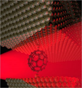
Getting back to the buckyball, the researchers have provided an image to illustrate their work,

Rice University scientists discovered the bonds in a carbon-60 molecule – a buckyball – can be "detuned" when exposed to an electric current in an optical antenna. (Credit: Natelson Group/Rice University)

Rice University scientists discovered the bonds in a carbon-60 molecule – a buckyball – can be “detuned” when exposed to an electric current in an optical antenna. (Credit: Natelson Group/Rice University)