Tag Archives: topological insulators

Brain-like computing and memory with magnetoresistance

This is an approach to brain-like computing that’s new (to me, anyway). From a January 9, 2018 news item on Nanowerk (Note: A link has been removed),

From various magnetic tapes, floppy disks and computer hard disk drives, magnetic materials have been storing our electronic information along with our valuable knowledge and memories for well over half of a century.

In more recent years, the new types [sic] phenomena known as magnetoresistance, which is the tendency of a material to change its electrical resistance when an externally-applied magnetic field or its own magnetization is changed, has found its success in hard disk drive read heads, magnetic field sensors and the rising star in the memory technologies, the magnetoresistive random access memory.

A new discovery, led by researchers at the University of Minnesota, demonstrates the existence of a new kind of magnetoresistance involving topological insulators that could result in improvements in future computing and computer storage. The details of their research are published in the most recent issue of the scientific journal Nature Communications (“Unidirectional spin-Hall and Rashba-Edelstein magnetoresistance in topological insulator-ferromagnet layer heterostructures”).

This image illustrates the work,

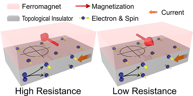
The schematic figure illustrates the concept and behavior of magnetoresistance. The spins are generated in topological insulators. Those at the interface between ferromagnet and topological insulators interact with the ferromagnet and result in either high or low resistance of the device, depending on the relative directions of magnetization and spins. Credit: University of Minnesota

A January 9, 2018 University of Minnesota College of Science and Engineering news release, which originated the news item, expands on the theme,

“Our discovery is one missing piece of the puzzle to improve the future of low-power computing and memory for the semiconductor industry, including brain-like computing and chips for robots and 3D magnetic memory,” said University of Minnesota Robert F. Hartmann Professor of Electrical and Computer Engineering Jian-Ping Wang, director of the Center for Spintronic Materials, Interfaces, and Novel Structures (C-SPIN) based at the University of Minnesota and co-author of the study.

Emerging technology using topological insulators

While magnetic recording still dominates data storage applications, the magnetoresistive random access memory is gradually finding its place in the field of computing memory. From the outside, they are unlike the hard disk drives which have mechanically spinning disks and swinging heads—they are more like any other type of memory. They are chips (solid state) which you’d find being soldered on circuit boards in a computer or mobile device.

Recently, a group of materials called topological insulators has been found to further improve the writing energy efficiency of magnetoresistive random access memory cells in electronics. However, the new device geometry demands a new magnetoresistance phenomenon to accomplish the read function of the memory cell in 3D system and network.

Following the recent discovery of the unidirectional spin Hall magnetoresistance in a conventional metal bilayer material systems, researchers at the University of Minnesota collaborated with colleagues at Pennsylvania State University and demonstrated for the first time the existence of such magnetoresistance in the topological insulator-ferromagnet bilayers.

The study confirms the existence of such unidirectional magnetoresistance and reveals that the adoption of topological insulators, compared to heavy metals, doubles the magnetoresistance performance at 150 Kelvin (-123.15 Celsius). From an application perspective, this work provides the missing piece of the puzzle to create a proposed 3D and cross-bar type computing and memory device involving topological insulators by adding the previously missing or very inconvenient read functionality.

In addition to Wang, researchers involved in this study include Yang Lv, Delin Zhang and Mahdi Jamali from the University of Minnesota Department of Electrical and Computer Engineering and James Kally, Joon Sue Lee and Nitin Samarth from Pennsylvania State University Department of Physics.

This research was funded by the Center for Spintronic Materials, Interfaces and Novel Architectures (C-SPIN) at the University of Minnesota, a Semiconductor Research Corporation program sponsored by the Microelectronics Advanced Research Corp. (MARCO) and the Defense Advanced Research Projects Agency (DARPA).

Here’s a link to and a citation for the paper,

Unidirectional spin-Hall and Rashba−Edelstein magnetoresistance in topological insulator-ferromagnet layer heterostructures by Yang Lv, James Kally, Delin Zhang, Joon Sue Lee, Mahdi Jamali, Nitin Samarth, & Jian-Ping Wang. Nature Communications 9, Article number: 111 (2018) doi:10.1038/s41467-017-02491-3 Published online: 09 January 2018

This is an open access paper.

New form of light could lead to circuits that run on photons instead of electrons

If circuits are running on photons instead of electrons, does that mean there will be no more electricity and electronics?  Apparently, the answer is not exactly. First, an Aug. 5, 2016 news item on ScienceDaily makes the announcement about photons and circuits,

New research suggests that it is possible to create a new form of light by binding light to a single electron, combining the properties of both.

According to the scientists behind the study, from Imperial College London, the coupled light and electron would have properties that could lead to circuits that work with packages of light — photons — instead of electrons.

It would also allow researchers to study quantum physical phenomena, which govern particles smaller than atoms, on a visible scale.

An Aug. 5, 2016 Imperial College of London (ICL) press release, which originated the news item, describes the research further (Note: A link has been removed),

In normal materials, light interacts with a whole host of electrons present on the surface and within the material. But by using theoretical physics to model the behaviour of light and a recently-discovered class of materials known as topological insulators, Imperial researchers have found that it could interact with just one electron on the surface.

This would create a coupling that merges some of the properties of the light and the electron. Normally, light travels in a straight line, but when bound to the electron it would instead follow its path, tracing the surface of the material.

Improved electronics

In the study, published today in Nature Communications, Dr Vincenzo Giannini and colleagues modelled this interaction around a nanoparticle – a small sphere below 0.00000001 metres in diameter – made of a topological insulator.

Their models showed that as well as the light taking the property of the electron and circulating the particle, the electron would also take on some of the properties of the light. [emphasis mine]

Normally, as electrons are travelling along materials, such as electrical circuits, they will stop when faced with a defect. However, Dr Giannini’s team discovered that even if there were imperfections in the surface of the nanoparticle, the electron would still be able to travel onwards with the aid of the light.

If this could be adapted into photonic circuits, they would be more robust and less vulnerable to disruption and physical imperfections.

Quantum experiments

Dr Giannini said: “The results of this research will have a huge impact on the way we conceive light. Topological insulators were only discovered in the last decade, but are already providing us with new phenomena to study and new ways to explore important concepts in physics.”

Dr Giannini added that it should be possible to observe the phenomena he has modelled in experiments using current technology, and the team is working with experimental physicists to make this a reality.

He believes that the process that leads to the creation of this new form of light could be scaled up so that the phenomena could observed much more easily.

Currently, quantum phenomena can only be seen when looking at very small objects or objects that have been super-cooled, but this could allow scientists to study these kinds of behaviour at room temperature.

An electron that takes on the properties of light? I find that fascinating.

Artistic image of light trapped on the surface of a nanoparticle topological insulator. Credit: Vincenzo Giannini

Artistic image of light trapped on the surface of a nanoparticle topological insulator. Credit: Vincenzo Giannini

For those who’d like more information, here’s a link to and a citation for the paper,

Single-electron induced surface plasmons on a topological nanoparticle by G. Siroki, D.K.K. Lee, P. D. Haynes,V. Giannini. Nature Communications 7, Article number: 12375  doi:10.1038/ncomms12375 Published 05 August 2016

This paper is open access.

Solving an iridescent mystery could lead to quantum transistors

iridescence has fascinated me (and scores of other people) since early childhood and it’s fascinating to note that scientists seems almost as enchanted as we amateurs are. The latest bit of ‘iridescent’ news comes from the University of Michigan in a Dec. 5, 2014 news item on ScienceDaily,

An odd, iridescent material that’s puzzled physicists for decades turns out to be an exotic state of matter that could open a new path to quantum computers and other next-generation electronics.

Physicists at the University of Michigan have discovered or confirmed several properties of the compound samarium hexaboride that raise hopes for finding the silicon of the quantum era. They say their results also close the case of how to classify the material–a mystery that has been investigated since the late 1960s.

A Dec. 5, 2014 University of Michigan news release, which originated the news item, provides more details about the mystery and the efforts to resolve it,

The researchers provide the first direct evidence that samarium hexaboride, abbreviated SmB6, is a topological insulator. Topological insulators are, to physicists, an exciting class of solids that conduct electricity like a metal across their surface, but block the flow of current like rubber through their interior. They behave in this two-faced way despite that their chemical composition is the same throughout.

The U-M scientists used a technique called torque magnetometry to observe tell-tale oscillations in the material’s response to a magnetic field that reveal how electric current moves through it. Their technique also showed that the surface of samarium hexaboride holds rare Dirac electrons, particles with the potential to help researchers overcome one of the biggest hurdles in quantum computing.

These properties are particularly enticing to scientists because SmB6 is considered a strongly correlated material. Its electrons interact more closely with one another than most solids. This helps its interior maintain electricity-blocking behavior.

This deeper understanding of samarium hexaboride raises the possibility that engineers might one day route the flow of electric current in quantum computers like they do on silicon in conventional electronics, said Lu Li, assistant professor of physics in the College of Literature, Science, and the Arts and a co-author of a paper on the findings published in Science.

“Before this, no one had found Dirac electrons in a strongly correlated material,” Li said. “We thought strong correlation would hurt them, but now we know it doesn’t. While I don’t think this material is the answer, now we know that this combination of properties is possible and we can look for other candidates.”

The drawback of samarium hexaboride is that the researchers only observed these behaviors at ultracold temperatures.

Quantum computers use particles like atoms or electrons to perform processing and memory tasks. They could offer dramatic increases in computing power due to their ability to carry out scores of calculations at once. Because they could factor numbers much faster than conventional computers, they would greatly improve computer security.

In quantum computers, “qubits” stand in for the 0s and 1s of conventional computers’ binary code. While a conventional bit can be either a 0 or a 1, a qubit could be both at the same time—only until you measure it, that is. Measuring a quantum system forces it to pick one state, which eliminates its main advantage.

Dirac electrons, named after the English physicist whose equations describe their behavior, straddle the realms of classical and quantum physics, Li said. Working together with other materials, they could be capable of clumping together into a new kind of qubit that would change the properties of a material in a way that could be measured indirectly, without the qubit sensing it. The qubit could remain in both states.

While these applications are intriguing, the researchers are most enthusiastic about the fundamental science they’ve uncovered.

“In the science business you have concepts that tell you it should be this or that and when it’s two things at once, that’s a sign you have something interesting to find,” said Jim Allen, an emeritus professor of physics who studied samarium hexaboride for 30 years. “Mysteries are always intriguing to people who do curiosity-driven research.”

Allen thought for years that samarium hexaboride must be a flawed insulator that behaved like a metal at low temperatures because of defects and impurities, but he couldn’t align that with all of its other properties.

“The prediction several years ago about it being a topological insulator makes a lightbulb go off if you’re an old guy like me and you’ve been living with this stuff your whole life,” Allen said.

In 2010, Kai Sun, assistant professor of physics at U-M, led a group that first posited that SmB6 might be a topological insulator. He and Allen were also involved in seminal U-M experiments led by physics professor Cagliyan Kurdak in 2012 that showed indirectly that the hypothesis was correct.

“But the scientific community is always critical,” Sun said. “They want very strong evidence. We think this experiment finally provides direct proof of our theory.”

Here’s a link to and a citation for the researchers’ latest paper,

Two-dimensional Fermi surfaces in Kondo insulator SmB6 by G. Li, Z. Xiang, F. Yu, T. Asaba, B. Lawson, P. Cai1, C. Tinsman, A. Berkley, S. Wolgast, Y. S. Eo, Dae-Jeong Kim, C. Kurdak, J. W. Allen, K. Sun, X. H. Chen, Y. Y. Wang, Z. Fisk, and Lu Li. Science 5 December 2014: Vol. 346 no. 6214 pp. 1208-1212 DOI: 10.1126/science.1250366

This paper is behind a paywall.

Adventures in time, mass, and topological insulators

Nano at a billionth (of a second, or a metre, or some other measure) is not the smallest unit of measurement, despite how we often talk about nano ‘anything’. But, as we continue to explore matter at ever more subtle levels, we need ever smaller units of measure and there are some ready for use.

I have a few excerpts from a Sept. 18, 2012  article (Explained: Femtoseconds and attoseconds) by David Chandler at the Massachusetts Institute of Technology (MIT) describing some of these smaller units of measure and how they were devised,

Back in the first half of the 20th century, when MIT’s famed Harold “Doc” Edgerton was perfecting his system for capturing fast-moving events on film, the ability to observe changes unfolding at a scale of microseconds — millionths of a second — was considered a remarkable achievement. This led to now-famous images such as one of a bullet piercing an apple, captured in midflight.

Nowadays, microsecond-resolution imagery is almost ho-hum. The cutting edge of research passed through nanoseconds (billionths of a second) and picoseconds (trillionths) in the 1970s and 1980s. Today, researchers can easily reach into the realm of femtoseconds — quadrillionths (or millionths of a billionth) of a second, the timescale of motions within molecules.

Femtosecond laser research led to the development, in 2000, of a system that revolutionized the measurement of optical frequencies and enabled optical clocks. Continuing the progress, today’s top-shelf technologies are beginning to make it possible to observe events that last less than 100 attoseconds, or quintillionths of a second.

Those prefixes — micro, nano, pico, femto and atto — are part of an internationally agreed-upon system called SI units (from the French Système International d’Unités, or International System of Units). The system was officially adopted in 1960, and has been updated periodically, most recently in 1991. It encompasses a total of 20 prefixes, 10 of them for decimal amounts, and 10 more for large multiples of the basic units (mega, giga, tera and so on).

As Chandler points out in more detail than I have, there’s a reason for developing these units of measure,

The ability to observe events on such timescales is important for basic physics — to understand how atoms move within molecules — as well as for engineering semiconductor devices, and for understanding basic biological processes at the molecular level.

But physicists and engineers are interested in pushing these limits ever further. To understand the movements of electrons, and eventually those of subatomic particles, requires attaining the attosecond and ultimately zeptosecond (sextillionths of a second) range, Kaertner says. Achieving that requires pushing technology to produce pulses using higher-wavelength sources, and also producing pulses that encompass a wider range of frequencies — a more broadband source.

I finally managed to conceptualize the nanoscale a few years ago but it appears I have more work to do. Chandler offers some suggestions for imagining the femtoscale,

So, just how short is a femtosecond? One way to think of it, Kaertner [Franz Kaertner, MIT adjunct professor of electrical engineering] says, is in terms of how far light can move in a given amount of time. Light travels about 300,000 kilometers (or 186,000 miles) in one second. That means it goes about 30 centimeters — about one foot — in one nanosecond. In one femtosecond, light travels just 300 nanometers — about the size of the biggest particle that can pass through a HEPA filter, and just slightly larger than the smallest bacteria.

Another way of thinking about the length of a femtosecond is this: One femtosecond is to one second as one second is to about 32 million years.

Chandler discuses in another MIT article (Watching electrons move at high speed) also posted on Sept. 18, 2012, a new electronic material, a topological insulator, and the importance of viewing the behaviour of electrons present in such an insulator,

Topological insulators are exotic materials, discovered just a few years ago, that hold great promise for new kinds of electronic devices. The unusual behavior of electrons within them has been very difficult to study, but new techniques developed by a team of researchers at MIT could help unlock the mysteries of exactly how electrons move and react in these materials, opening up new possibilities for harnessing them.

For the first time, the MIT team has managed to create three-dimensional “movies” of electron behavior in a topological insulator, or TI. [can be viewed here] The movies can capture vanishingly small increments of time — down to the level of a few femtoseconds, or millionths of a billionth of a second — so that they can catch the motions of electrons as they scatter in response to a very short pulse of light.

Electrons normally have mass, just like many other fundamental particles, but when moving along the surface of TIs they move as if they were massless, like light — one of the extraordinary characteristics that give these new materials such promise for new technologies. [emphases mine]

It’s the bit about mass and masslessness that caught my eye. Fascincating, non? Here’s a graphical representation of what the MIT scientists observed (I think it looks like a cup or a grail),

Three-dimensional graphical representations of the way electrons respond to an input of energy, delivered by a pulse of laser light. The horizontal axis represents the electrons’ momentum, and the vertical axis shows their energy. The time sequence runs from top left to bottom right, and the laser pulse arrives just before the second image, causing a sudden burst of higher energy levels. Images courtesy of Yihua Wang and Nuh Gedik [of MIT]

Here’s a bit more about TIs and possible future applications,

TIs are a class of materials with seemingly contradictory characteristics: The bulk of the material acts as an insulator, almost completely blocking any flow of electrons. But the surface of the material behaves as a very good conductor, like a metal, allowing electrons to travel freely. In fact, the surface is even more conductive than normal metals — allowing electrons to travel at almost the speed of light and to be unaffected by impurities in the material, which normally hinder their motion.

Because of these characteristics, TIs are seen as a promising new material for electronic circuits and data-storage devices. But developing such new devices requires a better understanding of exactly how electrons move around on and inside the TI, and how the surface electrons interact with those inside the material.

I highly recommend reading both of Chandler’s articles.