Tag Archives: UC Santa Barbara

Quantum supremacy

This supremacy, refers to an engineering milestone and a October 23, 2019 news item on ScienceDaily announces the milestone has been reached,

Researchers in UC [University of California] Santa Barbara/Google scientist John Martinis’ group have made good on their claim to quantum supremacy. Using 53 entangled quantum bits (“qubits”), their Sycamore computer has taken on — and solved — a problem considered intractable for classical computers.

An October 23, 2019 UC Santa Barbara news release (also on EurekAlert) by Sonia Fernandez, which originated the news item, delves further into the work,

“A computation that would take 10,000 years on a classical supercomputer took 200 seconds on our quantum computer,” said Brooks Foxen, a graduate student researcher in the Martinis Group. “It is likely that the classical simulation time, currently estimated at 10,000 years, will be reduced by improved classical hardware and algorithms, but, since we are currently 1.5 trillion times faster, we feel comfortable laying claim to this achievement.”

The feat is outlined in a paper in the journal Nature.

The milestone comes after roughly two decades of quantum computing research conducted by Martinis and his group, from the development of a single superconducting qubit to systems including architectures of 72 and, with Sycamore, 54 qubits (one didn’t perform) that take advantage of the both awe-inspiring and bizarre properties of quantum mechanics.

“The algorithm was chosen to emphasize the strengths of the quantum computer by leveraging the natural dynamics of the device,” said Ben Chiaro, another graduate student researcher in the Martinis Group. That is, the researchers wanted to test the computer’s ability to hold and rapidly manipulate a vast amount of complex, unstructured data.

“We basically wanted to produce an entangled state involving all of our qubits as quickly as we can,” Foxen said, “and so we settled on a sequence of operations that produced a complicated superposition state that, when measured, returns bitstring with a probability determined by the specific sequence of operations used to prepare that particular superposition. The exercise, which was to verify that the circuit’s output correspond to the equence used to prepare the state, sampled the quantum circuit a million times in just a few minutes, exploring all possibilities — before the system could lose its quantum coherence.

‘A complex superposition state’

“We performed a fixed set of operations that entangles 53 qubits into a complex superposition state,” Chiaro explained. “This superposition state encodes the probability distribution. For the quantum computer, preparing this superposition state is accomplished by applying a sequence of tens of control pulses to each qubit in a matter of microseconds. We can prepare and then sample from this distribution by measuring the qubits a million times in 200 seconds.”

“For classical computers, it is much more difficult to compute the outcome of these operations because it requires computing the probability of being in any one of the 2^53 possible states, where the 53 comes from the number of qubits — the exponential scaling is why people are interested in quantum computing to begin with,” Foxen said. “This is done by matrix multiplication, which is expensive for classical computers as the matrices become large.”

According to the new paper, the researchers used a method called cross-entropy benchmarking to compare the quantum circuit’s output (a “bitstring”) to its “corresponding ideal probability computed via simulation on a classical computer” to ascertain that the quantum computer was working correctly.

“We made a lot of design choices in the development of our processor that are really advantageous,” said Chiaro. Among these advantages, he said, are the ability to experimentally tune the parameters of the individual qubits as well as their interactions.

While the experiment was chosen as a proof-of-concept for the computer, the research has resulted in a very real and valuable tool: a certified random number generator. Useful in a variety of fields, random numbers can ensure that encrypted keys can’t be guessed, or that a sample from a larger population is truly representative, leading to optimal solutions for complex problems and more robust machine learning applications. The speed with which the quantum circuit can produce its randomized bit string is so great that there is no time to analyze and “cheat” the system.

“Quantum mechanical states do things that go beyond our day-to-day experience and so have the potential to provide capabilities and application that would otherwise be unattainable,” commented Joe Incandela, UC Santa Barbara’s vice chancellor for research. “The team has demonstrated the ability to reliably create and repeatedly sample complicated quantum states involving 53 entangled elements to carry out an exercise that would take millennia to do with a classical supercomputer. This is a major accomplishment. We are at the threshold of a new era of knowledge acquisition.”

Looking ahead

With an achievement like “quantum supremacy,” it’s tempting to think that the UC Santa Barbara/Google researchers will plant their flag and rest easy. But for Foxen, Chiaro, Martinis and the rest of the UCSB/Google AI Quantum group, this is just the beginning.

“It’s kind of a continuous improvement mindset,” Foxen said. “There are always projects in the works.” In the near term, further improvements to these “noisy” qubits may enable the simulation of interesting phenomena in quantum mechanics, such as thermalization, or the vast amount of possibility in the realms of materials and chemistry.

In the long term, however, the scientists are always looking to improve coherence times, or, at the other end, to detect and fix errors, which would take many additional qubits per qubit being checked. These efforts have been running parallel to the design and build of the quantum computer itself, and ensure the researchers have a lot of work before hitting their next milestone.

“It’s been an honor and a pleasure to be associated with this team,” Chiaro said. “It’s a great collection of strong technical contributors with great leadership and the whole team really synergizes well.”

Here’s a link to and a citation for the paper,

Quantum supremacy using a programmable superconducting processor by Frank Arute, Kunal Arya, Ryan Babbush, Dave Bacon, Joseph C. Bardin, Rami Barends, Rupak Biswas, Sergio Boixo, Fernando G. S. L. Brandao, David A. Buell, Brian Burkett, Yu Chen, Zijun Chen, Ben Chiaro, Roberto Collins, William Courtney, Andrew Dunsworth, Edward Farhi, Brooks Foxen, Austin Fowler, Craig Gidney, Marissa Giustina, Rob Graff, Keith Guerin, Steve Habegger, Matthew P. Harrigan, Michael J. Hartmann, Alan Ho, Markus Hoffmann, Trent Huang, Travis S. Humble, Sergei V. Isakov, Evan Jeffrey, Zhang Jiang, Dvir Kafri, Kostyantyn Kechedzhi, Julian Kelly, Paul V. Klimov, Sergey Knysh, Alexander Korotkov, Fedor Kostritsa, David Landhuis, Mike Lindmark, Erik Lucero, Dmitry Lyakh, Salvatore Mandrà, Jarrod R. McClean, Matthew McEwen, Anthony Megrant, Xiao Mi, Kristel Michielsen, Masoud Mohseni, Josh Mutus, Ofer Naaman, Matthew Neeley, Charles Neill, Murphy Yuezhen Niu, Eric Ostby, Andre Petukhov, John C. Platt, Chris Quintana, Eleanor G. Rieffel, Pedram Roushan, Nicholas C. Rubin, Daniel Sank, Kevin J. Satzinger, Vadim Smelyanskiy, Kevin J. Sung, Matthew D. Trevithick, Amit Vainsencher, Benjamin Villalonga, Theodore White, Z. Jamie Yao, Ping Yeh, Adam Zalcman, Hartmut Neven & John M. Martinis. Nature volume 574, pages505–510 (2019) DOI: https://doi.org/10.1038/s41586-019-1666-5 Issue Date 24 October 2019

This paper appears to be open access.
The memristor as computing device

An Oct. 27, 2016 news item on Nanowerk both builds on the Richard Feynman legend/myth and announces some new work with memristors,

In 1959 renowned physicist Richard Feynman, in his talk “[There’s] Plenty of Room at the Bottom,” spoke of a future in which tiny machines could perform huge feats. Like many forward-looking concepts, his molecule and atom-sized world remained for years in the realm of science fiction.

And then, scientists and other creative thinkers began to realize Feynman’s nanotechnological visions.

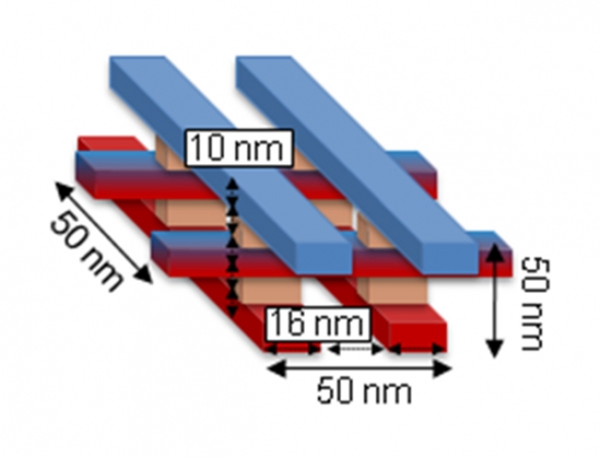
In the spirit of Feynman’s insight, and in response to the challenges he issued as a way to inspire scientific and engineering creativity, electrical and computer engineers at UC Santa Barbara [University of California at Santa Barbara, UCSB] have developed a design for a functional nanoscale computing device. The concept involves a dense, three-dimensional circuit operating on an unconventional type of logic that could, theoretically, be packed into a block no bigger than 50 nanometers on any side.

A figure depicting the structure of stacked memristors with dimensions that could satisfy the Feynman Grand Challenge Photo Credit: Courtesy Image

A figure depicting the structure of stacked memristors with dimensions that could satisfy the Feynman Grand Challenge. Photo Credit: Courtesy Image

An Oct. 27, 2016 UCSB news release (also on EurekAlert) by Sonia Fernandez, which originated the news item, offers a basic explanation of the work (useful for anyone unfamiliar with memristors) along with more detail,

“Novel computing paradigms are needed to keep up with the demand for faster, smaller and more energy-efficient devices,” said Gina Adam, postdoctoral researcher at UCSB’s Department of Computer Science and lead author of the paper “Optimized stateful material implication logic for three dimensional data manipulation,” published in the journal Nano Research. “In a regular computer, data processing and memory storage are separated, which slows down computation. Processing data directly inside a three-dimensional memory structure would allow more data to be stored and processed much faster.”

While efforts to shrink computing devices have been ongoing for decades — in fact, Feynman’s challenges as he presented them in his 1959 talk have been met — scientists and engineers continue to carve out room at the bottom for even more advanced nanotechnology. A nanoscale 8-bit adder operating in 50-by-50-by-50 nanometer dimension, put forth as part of the current Feynman Grand Prize challenge by the Foresight Institute, has not yet been achieved. However, the continuing development and fabrication of progressively smaller components is bringing this virus-sized computing device closer to reality, said Dmitri Strukov, a UCSB professor of computer science.

“Our contribution is that we improved the specific features of that logic and designed it so it could be built in three dimensions,” he said.

Key to this development is the use of a logic system called material implication logic combined with memristors — circuit elements whose resistance depends on the most recent charges and the directions of those currents that have flowed through them. Unlike the conventional computing logic and circuitry found in our present computers and other devices, in this form of computing, logic operation and information storage happen simultaneously and locally. This greatly reduces the need for components and space typically used to perform logic operations and to move data back and forth between operation and memory storage. The result of the computation is immediately stored in a memory element, which prevents data loss in the event of power outages — a critical function in autonomous systems such as robotics.

In addition, the researchers reconfigured the traditionally two-dimensional architecture of the memristor into a three-dimensional block, which could then be stacked and packed into the space required to meet the Feynman Grand Prize Challenge.

“Previous groups show that individual blocks can be scaled to very small dimensions, let’s say 10-by-10 nanometers,” said Strukov, who worked at technology company Hewlett-Packard’s labs when they ramped up development of memristors and material implication logic. By applying those results to his group’s developments, he said, the challenge could easily be met.

The tiny memristors are being heavily researched in academia and in industry for their promising uses in memory storage and neuromorphic computing. While implementations of material implication logic are rather exotic and not yet mainstream, uses for it could pop up any time, particularly in energy scarce systems such as robotics and medical implants.

“Since this technology is still new, more research is needed to increase its reliability and lifetime and to demonstrate large scale three-dimensional circuits tightly packed in tens or hundreds of layers,” Adam said.

HP Labs, mentioned in the news release, announced the ‘discovery’ of memristors and subsequent application of engineering control in two papers in 2008.

Here’s a link to and a citation for the UCSB paper,

Optimized stateful material implication logic for threedimensional data manipulation by Gina C. Adam, Brian D. Hoskins, Mirko Prezioso, &Dmitri B. Strukov. Nano Res. (2016) pp. 1 – 10. doi:10.1007/s12274-016-1260-1 First Online: 29 September 2016

This paper is behind a paywall.

You can find many articles about memristors here by using either ‘memristor’ or ‘memristors’ as your search term.

Ocean-inspired coatings for organic electronics

An Oct. 19, 2016 news item on phys.org describes the advantages a new coating offers and the specific source of inspiration,

In a development beneficial for both industry and environment, UC Santa Barbara [University of California at Santa Barbara] researchers have created a high-quality coating for organic electronics that promises to decrease processing time as well as energy requirements.

“It’s faster, and it’s nontoxic,” said Kollbe Ahn, a research faculty member at UCSB’s Marine Science Institute and corresponding author of a paper published in Nano Letters.

In the manufacture of polymer (also known as “organic”) electronics—the technology behind flexible displays and solar cells—the material used to direct and move current is of supreme importance. Since defects reduce efficiency and functionality, special attention must be paid to quality, even down to the molecular level.

Often that can mean long processing times, or relatively inefficient processes. It can also mean the use of toxic substances. Alternatively, manufacturers can choose to speed up the process, which could cost energy or quality.

Fortunately, as it turns out, efficiency, performance and sustainability don’t always have to be traded against each other in the manufacture of these electronics. Looking no further than the campus beach, the UCSB researchers have found inspiration in the mollusks that live there. Mussels, which have perfected the art of clinging to virtually any surface in the intertidal zone, serve as the model for a molecularly smooth, self-assembled monolayer for high-mobility polymer field-effect transistors—in essence, a surface coating that can be used in the manufacture and processing of the conductive polymer that maintains its efficiency.

An Oct. 18, 2016 UCSB news release by Sonia Fernandez, which originated the news item, provides greater technical detail,

More specifically, according to Ahn, it was the mussel’s adhesion mechanism that stirred the researchers’ interest. “We’re inspired by the proteins at the interface between the plaque and substrate,” he said.

Before mussels attach themselves to the surfaces of rocks, pilings or other structures found in the inhospitable intertidal zone, they secrete proteins through the ventral grove of their feet, in an incremental fashion. In a step that enhances bonding performance, a thin priming layer of protein molecules is first generated as a bridge between the substrate and other adhesive proteins in the plaques that tip the byssus threads of their feet to overcome the barrier of water and other impurities.

That type of zwitterionic molecule — with both positive and negative charges — inspired by the mussel’s native proteins (polyampholytes), can self-assemble and form a sub-nano thin layer in water at ambient temperature in a few seconds. The defect-free monolayer provides a platform for conductive polymers in the appropriate direction on various dielectric surfaces.

Current methods to treat silicon surfaces (the most common dielectric surface), for the production of organic field-effect transistors, requires a batch processing method that is relatively impractical, said Ahn. Although heat can hasten this step, it involves the use of energy and increases the risk of defects.

With this bio-inspired coating mechanism, a continuous roll-to-roll dip coating method of producing organic electronic devices is possible, according to the researchers. It also avoids the use of toxic chemicals and their disposal, by replacing them with water.

“The environmental significance of this work is that these new bio-inspired primers allow for nanofabrication on silicone dioxide surfaces in the absence of organic solvents, high reaction temperatures and toxic reagents,” said co-author Roscoe Lindstadt, a graduate student researcher in UCSB chemistry professor Bruce Lipshutz’s lab. “In order for practitioners to switch to newer, more environmentally benign protocols, they need to be competitive with existing ones, and thankfully device performance is improved by using this ‘greener’ method.”

Here’s a link to and a citation for the research paper,

Molecularly Smooth Self-Assembled Monolayer for High-Mobility Organic Field-Effect Transistors by Saurabh Das, Byoung Hoon Lee, Roscoe T. H. Linstadt, Keila Cunha, Youli Li, Yair Kaufman, Zachary A. Levine, Bruce H. Lipshutz, Roberto D. Lins, Joan-Emma Shea, Alan J. Heeger, and B. Kollbe Ahn. Nano Lett., 2016, 16 (10), pp 6709–6715
DOI: 10.1021/acs.nanolett.6b03860 Publication Date (Web): September 27, 2016

Copyright © 2016 American Chemical Society

This paper is behind a paywall but the scientists have made an illustration available,

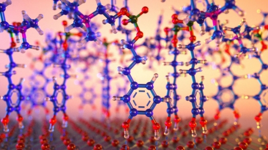
An artist's concept of a zwitterionic molecule of the type secreted by mussels to prime surfaces for adhesion Photo Credit: Peter Allen

An artist’s concept of a zwitterionic molecule of the type secreted by mussels to prime surfaces for adhesion Photo Credit: Peter Allen

Connecting chaos and entanglement

Researchers seem to have stumbled across a link between classical and quantum physics. A July 12, 2016 University of California at Santa Barbara (UCSB) news release (also on EurekAlert) by Sonia Fernandez provides a description of both classical and quantum physics, as well as, the research that connects the two,

Using a small quantum system consisting of three superconducting qubits, researchers at UC Santa Barbara and Google have uncovered a link between aspects of classical and quantum physics thought to be unrelated: classical chaos and quantum entanglement. Their findings suggest that it would be possible to use controllable quantum systems to investigate certain fundamental aspects of nature.

“It’s kind of surprising because chaos is this totally classical concept — there’s no idea of chaos in a quantum system,” Charles Neill, a researcher in the UCSB Department of Physics and lead author of a paper that appears in Nature Physics. “Similarly, there’s no concept of entanglement within classical systems. And yet it turns out that chaos and entanglement are really very strongly and clearly related.”

Initiated in the 15th century, classical physics generally examines and describes systems larger than atoms and molecules. It consists of hundreds of years’ worth of study including Newton’s laws of motion, electrodynamics, relativity, thermodynamics as well as chaos theory — the field that studies the behavior of highly sensitive and unpredictable systems. One classic example of chaos theory is the weather, in which a relatively small change in one part of the system is enough to foil predictions — and vacation plans — anywhere on the globe.

At smaller size and length scales in nature, however, such as those involving atoms and photons and their behaviors, classical physics falls short. In the early 20th century quantum physics emerged, with its seemingly counterintuitive and sometimes controversial science, including the notions of superposition (the theory that a particle can be located in several places at once) and entanglement (particles that are deeply linked behave as such despite physical distance from one another).

And so began the continuing search for connections between the two fields.

All systems are fundamentally quantum systems, according [to] Neill, but the means of describing in a quantum sense the chaotic behavior of, say, air molecules in an evacuated room, remains limited.

Imagine taking a balloon full of air molecules, somehow tagging them so you could see them and then releasing them into a room with no air molecules, noted co-author and UCSB/Google researcher Pedram Roushan. One possible outcome is that the air molecules remain clumped together in a little cloud following the same trajectory around the room. And yet, he continued, as we can probably intuit, the molecules will more likely take off in a variety of velocities and directions, bouncing off walls and interacting with each other, resting after the room is sufficiently saturated with them.

“The underlying physics is chaos, essentially,” he said. The molecules coming to rest — at least on the macroscopic level — is the result of thermalization, or of reaching equilibrium after they have achieved uniform saturation within the system. But in the infinitesimal world of quantum physics, there is still little to describe that behavior. The mathematics of quantum mechanics, Roushan said, do not allow for the chaos described by Newtonian laws of motion.

To investigate, the researchers devised an experiment using three quantum bits, the basic computational units of the quantum computer. Unlike classical computer bits, which utilize a binary system of two possible states (e.g., zero/one), a qubit can also use a superposition of both states (zero and one) as a single state. Additionally, multiple qubits can entangle, or link so closely that their measurements will automatically correlate. By manipulating these qubits with electronic pulses, Neill caused them to interact, rotate and evolve in the quantum analog of a highly sensitive classical system.

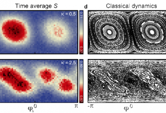
The result is a map of entanglement entropy of a qubit that, over time, comes to strongly resemble that of classical dynamics — the regions of entanglement in the quantum map resemble the regions of chaos on the classical map. The islands of low entanglement in the quantum map are located in the places of low chaos on the classical map.

“There’s a very clear connection between entanglement and chaos in these two pictures,” said Neill. “And, it turns out that thermalization is the thing that connects chaos and entanglement. It turns out that they are actually the driving forces behind thermalization.

“What we realize is that in almost any quantum system, including on quantum computers, if you just let it evolve and you start to study what happens as a function of time, it’s going to thermalize,” added Neill, referring to the quantum-level equilibration. “And this really ties together the intuition between classical thermalization and chaos and how it occurs in quantum systems that entangle.”

The study’s findings have fundamental implications for quantum computing. At the level of three qubits, the computation is relatively simple, said Roushan, but as researchers push to build increasingly sophisticated and powerful quantum computers that incorporate more qubits to study highly complex problems that are beyond the ability of classical computing — such as those in the realms of machine learning, artificial intelligence, fluid dynamics or chemistry — a quantum processor optimized for such calculations will be a very powerful tool.

“It means we can study things that are completely impossible to study right now, once we get to bigger systems,” said Neill.

Experimental link between quantum entanglement (left) and classical chaos (right) found using a small quantum computer. Photo Credit: Courtesy Image (Courtesy: UCSB)

Experimental link between quantum entanglement (left) and classical chaos (right) found using a small quantum computer. Photo Credit: Courtesy Image (Courtesy: UCSB)

Here’s a link to and a citation for the paper,

Ergodic dynamics and thermalization in an isolated quantum system by C. Neill, P. Roushan, M. Fang, Y. Chen, M. Kolodrubetz, Z. Chen, A. Megrant, R. Barends, B. Campbell, B. Chiaro, A. Dunsworth, E. Jeffrey, J. Kelly, J. Mutus, P. J. J. O’Malley, C. Quintana, D. Sank, A. Vainsencher, J. Wenner, T. C. White, A. Polkovnikov, & J. M. Martinis. Nature Physics (2016)  doi:10.1038/nphys3830 Published online 11 July 2016

This paper is behind a paywall.

Memristor, memristor, you are popular

Regular readers know I have a long-standing interest in memristor and artificial brains. I have three memristor-related pieces of research,  published in the last month or so, for this post.

First, there’s some research into nano memory at RMIT University, Australia, and the University of California at Santa Barbara (UC Santa Barbara). From a May 12, 2015 news item on ScienceDaily,

RMIT University researchers have mimicked the way the human brain processes information with the development of an electronic long-term memory cell.

Researchers at the MicroNano Research Facility (MNRF) have built the one of the world’s first electronic multi-state memory cell which mirrors the brain’s ability to simultaneously process and store multiple strands of information.

The development brings them closer to imitating key electronic aspects of the human brain — a vital step towards creating a bionic brain — which could help unlock successful treatments for common neurological conditions such as Alzheimer’s and Parkinson’s diseases.

A May 11, 2015 RMIT University news release, which originated the news item, reveals more about the researchers’ excitement and about the research,

“This is the closest we have come to creating a brain-like system with memory that learns and stores analog information and is quick at retrieving this stored information,” Dr Sharath said.

“The human brain is an extremely complex analog computer… its evolution is based on its previous experiences, and up until now this functionality has not been able to be adequately reproduced with digital technology.”

The ability to create highly dense and ultra-fast analog memory cells paves the way for imitating highly sophisticated biological neural networks, he said.

The research builds on RMIT’s previous discovery where ultra-fast nano-scale memories were developed using a functional oxide material in the form of an ultra-thin film – 10,000 times thinner than a human hair.

Dr Hussein Nili, lead author of the study, said: “This new discovery is significant as it allows the multi-state cell to store and process information in the very same way that the brain does.

“Think of an old camera which could only take pictures in black and white. The same analogy applies here, rather than just black and white memories we now have memories in full color with shade, light and texture, it is a major step.”

While these new devices are able to store much more information than conventional digital memories (which store just 0s and 1s), it is their brain-like ability to remember and retain previous information that is exciting.

“We have now introduced controlled faults or defects in the oxide material along with the addition of metallic atoms, which unleashes the full potential of the ‘memristive’ effect – where the memory element’s behaviour is dependent on its past experiences,” Dr Nili said.

Nano-scale memories are precursors to the storage components of the complex artificial intelligence network needed to develop a bionic brain.

Dr Nili said the research had myriad practical applications including the potential for scientists to replicate the human brain outside of the body.

“If you could replicate a brain outside the body, it would minimise ethical issues involved in treating and experimenting on the brain which can lead to better understanding of neurological conditions,” Dr Nili said.

The research, supported by the Australian Research Council, was conducted in collaboration with the University of California Santa Barbara.

Here’s a link to and a citation for this memristive nano device,

Donor-Induced Performance Tuning of Amorphous SrTiO3 Memristive Nanodevices: Multistate Resistive Switching and Mechanical Tunability by  Hussein Nili, Sumeet Walia, Ahmad Esmaielzadeh Kandjani, Rajesh Ramanathan, Philipp Gutruf, Taimur Ahmed, Sivacarendran Balendhran, Vipul Bansal, Dmitri B. Strukov, Omid Kavehei, Madhu Bhaskaran, and Sharath Sriram. Advanced Functional Materials DOI: 10.1002/adfm.201501019 Article first published online: 14 APR 2015

© 2015 WILEY-VCH Verlag GmbH & Co. KGaA, Weinheim

This paper is behind a paywall.

The second published piece of memristor-related research comes from a UC Santa Barbara and  Stony Brook University (New York state) team but is being publicized by UC Santa Barbara. From a May 11, 2015 news item on Nanowerk (Note: A link has been removed),

In what marks a significant step forward for artificial intelligence, researchers at UC Santa Barbara have demonstrated the functionality of a simple artificial neural circuit (Nature, “Training and operation of an integrated neuromorphic network based on metal-oxide memristors”). For the first time, a circuit of about 100 artificial synapses was proved to perform a simple version of a typical human task: image classification.

A May 11, 2015 UC Santa Barbara news release (also on EurekAlert)by Sonia Fernandez, which originated the news item, situates this development within the ‘artificial brain’ effort while describing it in more detail (Note: A link has been removed),

“It’s a small, but important step,” said Dmitri Strukov, a professor of electrical and computer engineering. With time and further progress, the circuitry may eventually be expanded and scaled to approach something like the human brain’s, which has 1015 (one quadrillion) synaptic connections.

For all its errors and potential for faultiness, the human brain remains a model of computational power and efficiency for engineers like Strukov and his colleagues, Mirko Prezioso, Farnood Merrikh-Bayat, Brian Hoskins and Gina Adam. That’s because the brain can accomplish certain functions in a fraction of a second what computers would require far more time and energy to perform.

… As you read this, your brain is making countless split-second decisions about the letters and symbols you see, classifying their shapes and relative positions to each other and deriving different levels of meaning through many channels of context, in as little time as it takes you to scan over this print. Change the font, or even the orientation of the letters, and it’s likely you would still be able to read this and derive the same meaning.

In the researchers’ demonstration, the circuit implementing the rudimentary artificial neural network was able to successfully classify three letters (“z”, “v” and “n”) by their images, each letter stylized in different ways or saturated with “noise”. In a process similar to how we humans pick our friends out from a crowd, or find the right key from a ring of similar keys, the simple neural circuitry was able to correctly classify the simple images.

“While the circuit was very small compared to practical networks, it is big enough to prove the concept of practicality,” said Merrikh-Bayat. According to Gina Adam, as interest grows in the technology, so will research momentum.

“And, as more solutions to the technological challenges are proposed the technology will be able to make it to the market sooner,” she said.

Key to this technology is the memristor (a combination of “memory” and “resistor”), an electronic component whose resistance changes depending on the direction of the flow of the electrical charge. Unlike conventional transistors, which rely on the drift and diffusion of electrons and their holes through semiconducting material, memristor operation is based on ionic movement, similar to the way human neural cells generate neural electrical signals.

“The memory state is stored as a specific concentration profile of defects that can be moved back and forth within the memristor,” said Strukov. The ionic memory mechanism brings several advantages over purely electron-based memories, which makes it very attractive for artificial neural network implementation, he added.

“For example, many different configurations of ionic profiles result in a continuum of memory states and hence analog memory functionality,” he said. “Ions are also much heavier than electrons and do not tunnel easily, which permits aggressive scaling of memristors without sacrificing analog properties.”

This is where analog memory trumps digital memory: In order to create the same human brain-type functionality with conventional technology, the resulting device would have to be enormous — loaded with multitudes of transistors that would require far more energy.

“Classical computers will always find an ineluctable limit to efficient brain-like computation in their very architecture,” said lead researcher Prezioso. “This memristor-based technology relies on a completely different way inspired by biological brain to carry on computation.”

To be able to approach functionality of the human brain, however, many more memristors would be required to build more complex neural networks to do the same kinds of things we can do with barely any effort and energy, such as identify different versions of the same thing or infer the presence or identity of an object not based on the object itself but on other things in a scene.

Potential applications already exist for this emerging technology, such as medical imaging, the improvement of navigation systems or even for searches based on images rather than on text. The energy-efficient compact circuitry the researchers are striving to create would also go a long way toward creating the kind of high-performance computers and memory storage devices users will continue to seek long after the proliferation of digital transistors predicted by Moore’s Law becomes too unwieldy for conventional electronics.

Here’s a link to and a citation for the paper,

Training and operation of an integrated neuromorphic network based on metal-oxide memristors by M. Prezioso, F. Merrikh-Bayat, B. D. Hoskins, G. C. Adam, K. K. Likharev,    & D. B. Strukov. Nature 521, 61–64 (07 May 2015) doi:10.1038/nature14441

This paper is behind a paywall but a free preview is available through ReadCube Access.

The third and last piece of research, which is from Rice University, hasn’t received any publicity yet, unusual given Rice’s very active communications/media department. Here’s a link to and a citation for their memristor paper,

2D materials: Memristor goes two-dimensional by Jiangtan Yuan & Jun Lou. Nature Nanotechnology 10, 389–390 (2015) doi:10.1038/nnano.2015.94 Published online 07 May 2015

This paper is behind a paywall but a free preview is available through ReadCube Access.

Dexter Johnson has written up the RMIT research (his May 14, 2015 post on the Nanoclast blog on the IEEE [Institute of Electrical and Electronics Engineers] website). He linked it to research from Mark Hersam’s team at Northwestern University (my April 10, 2015 posting) on creating a three-terminal memristor enabling its use in complex electronics systems. Dexter strongly hints in his headline that these developments could lead to bionic brains.

For those who’d like more memristor information, this June 26, 2014 posting which brings together some developments at the University of Michigan and information about developments in the industrial sector is my suggestion for a starting point. Also, you may want to check out my material on HP Labs, especially prominent in the story due to the company’s 2008 ‘discovery’ of the memristor, described on a page in my Nanotech Mysteries wiki, and the controversy triggered by the company’s terminology (there’s more about the controversy in my April 7, 2010 interview with Forrest H Bennett III).

Structural color and cephalopods at the University of California Santa Barbara

I last wrote about structural color in a Feb.7, 2013 posting featuring a marvelous article on the topic by Cristina Luiggi in the The Scientist. As for cephalopods, one of my favourite postings on the topic is a Feb. 1, 2013 posting which features the giant squid, a newly discovered animal of mythical proportions that appears golden in its native habitat in the deep, deep ocean. Happily, there’s a July 25, 2013 news item on Nanowerk which combines structural color and squid,

Color in living organisms can be formed two ways: pigmentation or anatomical structure. Structural colors arise from the physical interaction of light with biological nanostructures. A wide range of organisms possess this ability, but the biological mechanisms underlying the process have been poorly understood.

Two years ago, an interdisciplinary team from UC Santa Barbara [University of California Santa Barbara a.k.a. UCSB] discovered the mechanism by which a neurotransmitter dramatically changes color in the common market squid, Doryteuthis opalescens. That neurotransmitter, acetylcholine, sets in motion a cascade of events that culminate in the addition of phosphate groups to a family of unique proteins called reflectins. This process allows the proteins to condense, driving the animal’s color-changing process.

The July 25, 2013 UC Santa Barbara news release (also on EurekAlert), which originated the news item, provides a good overview of the team’s work to date and the new work occasioning the news release,

Now the researchers have delved deeper to uncover the mechanism responsible for the dramatic changes in color used by such creatures as squids and octopuses. The findings –– published in the Proceedings of the National Academy of Science, in a paper by molecular biology graduate student and lead author Daniel DeMartini and co-authors Daniel V. Krogstad and Daniel E. Morse –– are featured in the current issue of The Scientist.

Structural colors rely exclusively on the density and shape of the material rather than its chemical properties. The latest research from the UCSB team shows that specialized cells in the squid skin called iridocytes contain deep pleats or invaginations of the cell membrane extending deep into the body of the cell. This creates layers or lamellae that operate as a tunable Bragg reflector. Bragg reflectors are named after the British father and son team who more than a century ago discovered how periodic structures reflect light in a very regular and predicable manner.

“We know cephalopods use their tunable iridescence for camouflage so that they can control their transparency or in some cases match the background,” said co-author Daniel E. Morse, Wilcox Professor of Biotechnology in the Department of Molecular, Cellular and Developmental Biology and director of the Marine Biotechnology Center/Marine Science Institute at UCSB.

“They also use it to create confusing patterns that disrupt visual recognition by a predator and to coordinate interactions, especially mating, where they change from one appearance to another,” he added. “Some of the cuttlefish, for example, can go from bright red, which means stay away, to zebra-striped, which is an invitation for mating.”

The researchers created antibodies to bind specifically to the reflectin proteins, which revealed that the reflectins are located exclusively inside the lamellae formed by the folds in the cell membrane. They showed that the cascade of events culminating in the condensation of the reflectins causes the osmotic pressure inside the lamellae to change drastically due to the expulsion of water, which shrinks and dehydrates the lamellae and reduces their thickness and spacing. The movement of water was demonstrated directly using deuterium-labeled heavy water.

When the acetylcholine neurotransmitter is washed away and the cell can recover, the lamellae imbibe water, rehydrating and allowing them to swell to their original thickness. This reversible dehydration and rehydration, shrinking and swelling, changes the thickness and spacing, which, in turn, changes the wavelength of the light that’s reflected, thus “tuning” the color change over the entire visible spectrum.

“This effect of the condensation on the reflectins simultaneously increases the refractive index inside the lamellae,” explained Morse. “Initially, before the proteins are consolidated, the refractive index –– you can think of it as the density –– inside the lamellae and outside, which is really the outside water environment, is the same. There’s no optical difference so there’s no reflection. But when the proteins consolidate, this increases the refractive index so the contrast between the inside and outside suddenly increases, causing the stack of lamellae to become reflective, while at the same time they dehydrate and shrink, which causes color changes. The animal can control the extent to which this happens –– it can pick the color –– and it’s also reversible. The precision of this tuning by regulating the nanoscale dimensions of the lamellae is amazing.”

Another paper by the same team of researchers, published in Journal of the Royal Society Interface, with optical physicist Amitabh Ghoshal as the lead author, conducted a mathematical analysis of the color change and confirmed that the changes in refractive index perfectly correspond to the measurements made with live cells.

A third paper, in press at Journal of Experimental Biology, reports the team’s discovery that female market squid show a set of stripes that can be brightly activated and may function during mating to allow the female to mimic the appearance of the male, thereby reducing the number of mating encounters and aggressive contacts from males. The most significant finding in this study is the discovery of a pair of stripes that switch from being completely transparent to bright white.

“This is the first time that switchable white cells based on the reflectin proteins have been discovered,” Morse noted. “The facts that these cells are switchable by the neurotransmitter acetylcholine, that they contain some of the same reflectin proteins, and that the reflectins are induced to condense to increase the refractive index and trigger the change in reflectance all suggest that they operate by a molecular mechanism fundamentally related to that controlling the tunable color.”

Could these findings one day have practical applications? “In telecommunications we’re moving to more rapid communication carried by light,” said Morse. “We already use optical cables and photonic switches in some of our telecommunications devices. The question is –– and it’s a question at this point –– can we learn from these novel biophotonic mechanisms that have evolved over millions of years of natural selection new approaches to making tunable and switchable photonic materials to more efficiently encode, transmit, and decode information via light?”

In fact, the UCSB researchers are collaborating with Raytheon Vision Systems in Goleta to investigate applications of their discoveries in the development of tunable filters and switchable shutters for infrared cameras. Down the road, there may also be possible applications for synthetic camouflage. [emphasis mine]

There is at least one other research team (the UK’s University of Bristol) considering the camouflage strategies employed cephalopods and, in their case,  zebra fish as noted in my May 4, 2012 posting, Camouflage for everyone.

Getting back to cephalopod in hand, here’s an image from the UC Santa Barbara team,

This shows the diffusion of the neurotransmitter applied to squid skin at upper right, which induces a wave of iridescence traveling to the lower left and progressing from red to blue. Each object in the image is a living cell, 10 microns long; the dark object in the center of each cell is the cell nucleus. [downloaded from http://www.ia.ucsb.edu/pa/display.aspx?pkey=3076]

This shows the diffusion of the neurotransmitter applied to squid skin at upper right, which induces a wave of iridescence traveling to the lower left and progressing from red to blue. Each object in the image is a living cell, 10 microns long; the dark object in the center of each cell is the cell nucleus. [downloaded from http://www.ia.ucsb.edu/pa/display.aspx?pkey=3076]

Fro papers currently available online, here are links and citations,

Optical parameters of the tunable Bragg reflectors in squid by Amitabh Ghoshal, Daniel G. DeMartini, Elizabeth Eck, and Daniel E. Morse. doi: 10.1098/​rsif.2013.0386 J. R. Soc. Interface 6 August 2013 vol. 10 no. 85 20130386

The Royal Society paper is behind a paywall until August 2014.

Membrane invaginations facilitate reversible water flux driving tunable iridescence in a dynamic biophotonic system by Daniel G. DeMartini, Daniel V. Krogstadb, and Daniel E. Morse. Published online before print January 28, 2013, doi: 10.1073/pnas.1217260110
PNAS February 12, 2013 vol. 110 no. 7 2552-2556

The Proceedings of the National Academy of Sciences (PNAS) paper (or the ‘Daniel’ paper as I prefer to think of it)  is behind a paywall.

Soybeans and nanoparticles

They seem ubiquitous today but there was a time when hardly anyone living in Canada  knew much about soybeans.  There’s a good essay about soybeans and their cultivation in Canada by Erik Dorff for Statistics Canada, from Dorff’s soybean essay,

Until the mid-1970s, soybeans were restricted by climate primarily to southern Ontario. Intensive breeding programs have since opened up more widespread growing possibilities across Canada for this incredibly versatile crop: The 1.2 million hectares of soybeans reported on the Census of Agriculture in 2006 marked a near eightfold increase in area since 1976, the year the ground-breaking varieties that perform well in Canada’s shorter growing season were introduced.

Soybeans have earned their popularity, with the high-protein, high-oil beans finding use as food for human consumption, animal rations and edible oils as well as many industrial products. Moreover, soybeans, like all legumes, are able to “fix” the nitrogen the plants need from the air. This process of nitrogen fixation is a result of a symbiotic interaction between bacteria microbes that colonize the roots of the soy plant and are fed by the plant. In return, the microbes take nitrogen from the air and convert it into a form the plant can use to grow.

This means legumes require little in the way of purchased nitrogen fertilizers produced from expensive natural gas-a valuable property indeed.

Until reading Dorff’s essay, I hadn’t early soybeans had been introduced to the Canadian agricultural sector,

While soybeans arrived in Canada in the mid 1800s-with growing trials recorded in 1893 at the Ontario Agricultural College-they didn’t become a commercial oilseed crop in Canada until a crushing plant was built in southern Ontario in the 1920s, about the same time that the Department of Agriculture (now Agriculture and Agri-Food Canada) began evaluating soybean varieties suited for the region. For years, soybeans were being grown in Canada but it wasn’t until the Second World War that Statistics Canada began to collect data showing the significance of the soybean crop, with 4,400 hectares being reported in 1941. In fact, one year later the area had jumped nearly fourfold, to 17,000 hectares…

As fascinating as I find this history, this bit about soybeans and their international importance explain why research about soyboans and nanoparticles is of wide interest (from Dorff’s essay),

The soybean’s valuable characteristics have propelled it into the agricultural mix in many parts of the world. In 2004, soybeans accounted for approximately 35% of the total harvested area worldwide of annual and perennial oil crops according to the Food and Agriculture Organization of the United Nations (FAO) but only four countries accounted for nearly 90% of the production with Canada in seventh place at 1.3% (Table 2). Soymeal-the solid, high-protein material remaining after the oil has been extracted during crushing-accounts for over 60% of world vegetable and animal meal production, while soybean oil accounts for 20% of global vegetable oil production.

There’s been a recent study on the impact of nanoparticles on soybeans at the University of California at Santa Barbara (UC Santa Barbara) according to an Aug. 20, 2012 posting by Alan on the Science Business website, (h/t to Cientifica),

Researchers from University of California in Santa Barbara found manufactured nanoparticles disposed after manufacturing or customer use can end up in agricultural soil and eventually affect soybean crops. Findings of the team that includes academic, government, and corporate researchers from elsewhere in California, Texas, Iowa, New York, and Korea appear online today in the Proceedings of the National Academy of Sciences.

The research aimed to discover potential environmental implications of new industries that produce nanomaterials. Soybeans were chosen as test crops because their prominence in American agriculture — it is the second largest crop in the U.S. and the fifth largest crop worldwide — and its vulnerability to manufactured nanomaterials. The soybeans tested in this study were grown in greenhouses.

The Aug. 20, 2012 UC Santa Barbara press release has additional detail abut why the research was undertaken,

“Our society has become more environmentally aware in the last few decades, and that results in our government and scientists asking questions about the safety of new types of chemical ingredients,” said senior author Patricia Holden, a professor with the Bren School [UC Santa Barbara’s Bren School of Environmental Science & Management]. “That’s reflected by this type of research.”

Soybean was chosen for the study due to its importance as a food crop –– it is the fifth largest crop in global agricultural production and second in the U.S. –– and because it is vulnerable to MNMs [manufactured nanomaterials]. The findings showed that crop yield and quality are affected by the addition of MNMs to the soil.

The scientists studied the effects of two common nanoparticles, zinc oxide and cerium oxide, on soybeans grown in soil in greenhouses. Zinc oxide is used in cosmetics, lotions, and sunscreens. Cerium oxide is used as an ingredient in catalytic converters to minimize carbon monoxide production, and in fuel to increase fuel combustion. Cerium can enter soil through the atmosphere when fuel additives are released with diesel fuel combustion.

The zinc oxide nanoparticles may dissolve, or they may remain as a particle, or re-form as a particle, as they are processed through wastewater treatment. At the final stage of wastewater treatment there is a solid material, called biosolids, which is applied to soils in many parts of the U.S. This solid material fertilizes the soil, returning nitrogen and phosphorus that are captured during wastewater treatment. This is also a point at which zinc oxide and cerium oxide can enter the soil.

The scientists noted that the EPA requires pretreatment programs to limit direct industrial metal discharge into publicly owned wastewater treatment plants. However, the research team conveyed that “MNMs –– while measurable in the wastewater treatment plant systems –– are neither monitored nor regulated, have a high affinity for activated sludge bacteria, and thus concentrate in biosolids.”

The authors pointed out that soybean crops are farmed with equipment powered by fossil fuels, and thus MNMs can also be deposited into the soil through exhaust.

The study showed that soybean plants grown in soil that contained zinc oxide bioaccumulated zinc; they absorbed it into the stems, leaves, and beans. Food quality was affected, although it may not be harmful to humans to eat the soybeans if the zinc is in the form of ions or salts, in the plants, according to Holden.

In the case of cerium oxide, the nanoparticles did not bioaccumulate, but plant growth was stunted. Changes occurred in the root nodules, where symbiotic bacteria normally accumulate and convert atmospheric nitrogen into ammonium, which fertilizes the plant. The changes in the root nodules indicate that greater use of synthetic fertilizers might be necessary with the buildup of MNMs in the soil.

At this point, the researchers don’t know how zinc oxide nanoparticles and cerium oxide nanoparticles currently used in consumer products and elsewhere are likely to affect agricultural lands. The only certainty is that these nanoparticles are used in consumer goods and, according to Holden, they are entering agricultural soil.

The citation for the article,

Soybean susceptibility to manufactured nanomaterials with evidence for food quality and soil fertility interruption by John H. Priester, Yuan Ge, Randall E. Mielke, Allison M. Horst Shelly Cole Moritz, Katherine Espinosa, Jeff Gelb, Sharon L. Walker, Roger M. Nisbet, Youn-Joo An, Joshua P. Schimel, Reid G. Palmer, Jose A. Hernandez-Viezcas, Lijuan Zhao, Jorge L. Gardea-Torresdey, Patricia A. Holden. Published online [Proceedings of the National Academy of Sciences {PNAS}] before print August 20, 2012, doi: 10.1073/pnas.1205431109

The article is open access and available here.