Tag Archives: UCSB

Thanks for the memory: the US National Institute of Standards and Technology (NIST) and memristors

In January 2018 it seemed like I was tripping across a lot of memristor stories . This came from a January 19, 2018 news item on Nanowerk,

In the race to build a computer that mimics the massive computational power of the human brain, researchers are increasingly turning to memristors, which can vary their electrical resistance based on the memory of past activity. Scientists at the National Institute of Standards and Technology (NIST) have now unveiled the long-mysterious inner workings of these semiconductor elements, which can act like the short-term memory of nerve cells.

A January 18, 2018 NIST news release (also on EurekAlert), which originated the news item, fills in the details,

Just as the ability of one nerve cell to signal another depends on how often the cells have communicated in the recent past, the resistance of a memristor depends on the amount of current that recently flowed through it. Moreover, a memristor retains that memory even when electrical power is switched off.

But despite the keen interest in memristors, scientists have lacked a detailed understanding of how these devices work and have yet to develop a standard toolset to study them.

Now, NIST scientists have identified such a toolset and used it to more deeply probe how memristors operate. Their findings could lead to more efficient operation of the devices and suggest ways to minimize the leakage of current.

Brian Hoskins of NIST and the University of California, Santa Barbara, along with NIST scientists Nikolai Zhitenev, Andrei Kolmakov, Jabez McClelland and their colleagues from the University of Maryland’s NanoCenter (link is external) in College Park and the Institute for Research and Development in Microtechnologies in Bucharest, reported the findings (link is external) in a recent Nature Communications.

To explore the electrical function of memristors, the team aimed a tightly focused beam of electrons at different locations on a titanium dioxide memristor. The beam knocked free some of the device’s electrons, which formed ultrasharp images of those locations. The beam also induced four distinct currents to flow within the device. The team determined that the currents are associated with the multiple interfaces between materials in the memristor, which consists of two metal (conducting) layers separated by an insulator.

“We know exactly where each of the currents are coming from because we are controlling the location of the beam that is inducing those currents,” said Hoskins.

In imaging the device, the team found several dark spots—regions of enhanced conductivity—which indicated places where current might leak out of the memristor during its normal operation. These leakage pathways resided outside the memristor’s core—where it switches between the low and high resistance levels that are useful in an electronic device. The finding suggests that reducing the size of a memristor could minimize or even eliminate some of the unwanted current pathways. Although researchers had suspected that might be the case, they had lacked experimental guidance about just how much to reduce the size of the device.

Because the leakage pathways are tiny, involving distances of only 100 to 300 nanometers, “you’re probably not going to start seeing some really big improvements until you reduce dimensions of the memristor on that scale,” Hoskins said.

To their surprise, the team also found that the current that correlated with the memristor’s switch in resistance didn’t come from the active switching material at all, but the metal layer above it. The most important lesson of the memristor study, Hoskins noted, “is that you can’t just worry about the resistive switch, the switching spot itself, you have to worry about everything around it.” The team’s study, he added, “is a way of generating much stronger intuition about what might be a good way to engineer memristors.”

Here’s a link to and a citation for the paper,

Stateful characterization of resistive switching TiO2 with electron beam induced currents by Brian D. Hoskins, Gina C. Adam, Evgheni Strelcov, Nikolai Zhitenev, Andrei Kolmakov, Dmitri B. Strukov, & Jabez J. McClelland. Nature Communications 8, Article number: 1972 (2017) doi:10.1038/s41467-017-02116-9 Published online: 07 December 2017

This is an open access paper.

It might be my imagination but it seemed like a lot of papers from 2017 were being publicized in early 2018.

Finally, I borrowed much of my headline from the NIST’s headline for its news release, specifically, “Thanks for the memory,” which is a rather old song,

Bob Hope and Shirley Ross in “The Big Broadcast of 1938.”

The Center for Nanotechnology in Society at the University of California at Santa Barbara offers a ‘swan song’ in three parts

I gather the University of California at Santa Barbara’s (UCSB) Center for Nanotechnology in Society is ‘sunsetting’ as its funding runs out. A Nov. 9, 2016 UCSB news release by Brandon Fastman describes the center’s ‘swan song’,

After more than a decade, the UCSB Center for Nanotechnology in Society research has provided new and deep knowledge of how technological innovation and social change impact one another. Now, as the national center reaches the end of its term, its three primary research groups have published synthesis reports that bring together important findings from their 11 years of activity.

The reports, which include policy recommendations, are available for free download at the CNS web site at

http://www.cns.ucsb.edu/irg-synthesis-reports.

The ever-increasing ability of scientists to manipulate matter on the molecular level brings with it the potential for science fiction-like technologies such as nanoelectronic sensors that would entail “merging tissue with electronics in a way that it becomes difficult to determine where the tissue ends and the electronics begin,” according to a Harvard chemist in a recent CQ Researcher report. While the life-altering ramifications of such technologies are clear, it is less clear how they might impact the larger society to which they are introduced.

CNS research, as detailed the reports, addresses such gaps in knowledge. For instance, when anthropologist Barbara Herr Harthorn and her collaborators at the UCSB Center for Nanotechnology in Society (CNS-UCSB), convened public deliberations to discuss the promises and perils of health and human enhancement nanotechnologies, they thought that participants might be concerned about medical risks. However, that is not exactly what they found.

Participants were less worried about medical or technological mishaps than about the equitable distribution of the risks and benefits of new technologies and fair procedures for addressing potential problems. That is, they were unconvinced that citizens across the socioeconomic spectrum would share equal access to the benefits of therapies or equal exposure to their pitfalls.

In describing her work, Harthorn explained, “Intuitive assumptions of experts and practitioners about public perceptions and concerns are insufficient to understanding the societal contexts of technologies. Relying on intuition often leads to misunderstandings of social and institutional realities. CNS-UCSB has attempted to fill in the knowledge gaps through methodologically sophisticated empirical and theoretical research.”

In her role as Director of CNS-UCSB, Harthorn has overseen a larger effort to promote the responsible development of sophisticated materials and technologies seen as central to the nation’s economic future. By pursuing this goal, researchers at CNS-UCSB, which closed its doors at the end of the summer, have advanced the role for the social, economic, and behavioral sciences in understanding technological innovation.

Harthorn has spent the past 11 years trying to understand public expectations, values, beliefs, and perceptions regarding nanotechnologies. Along with conducting deliberations, she has worked with toxicologists and engineers to examine the environmental and occupational risks of nanotechnologies, determine gaps in the U.S. regulatory system, and survey nanotechnology experts. Work has also expanded to comparative studies of other emerging technologies such as shale oil and gas extraction (fracking).

Along with Harthorn’s research group on risk perception and social response, CNS-UCSB housed two other main research groups. One, led by sociologist Richard Appelbaum, studied the impacts of nanotechnology on the global economy. The other, led by historian Patrick McCray, studied the technologies, communities, and individuals that have shaped the direction of nanotechnology research.

Appelbaum’s research program included studying how state policies regarding nanotechnology – especially in China and Latin America – has impacted commercialization. Research trips to China elicited a great understanding of that nation’s research culture and its capacity to produce original intellectual property. He also studied the role of international collaboration in spurring technological innovation. As part of this research, his collaborators surveyed and interviewed international STEM graduate students in the United States in order to understand the factors that influence their choice whether to remain abroad or return home.

In examining the history of nanotechnology, McCray’s group explained how the microelectronics industry provided a template for what became known as nanotechnology, examined educational policies aimed at training a nano-workforce, and produced a history of the scanning tunneling microscope. They also penned award-winning monographs including McCray’s book, The Visioneers: How a Group of Elite Scientists Pursued Space Colonies, Nanotechnologies, and Limitless Future.

Reaching the Real World

Funded as a National Center by the US National Science Foundation in 2005, CNS-UCSB was explicitly intended to enhance the understanding of the relationship between new technologies and their societal context. After more than a decade of funding, CNS-UCSB research has provided a deep understanding of the relationship between technological innovation and social change.

New developments in nanotechnology, an area of research that has garnered $24 billion in funding from the U.S. federal government since 2001, impact sectors as far ranging as agriculture, medicine, energy, defense, and construction, posing great challenges for policymakers and regulators who must consider questions of equity, sustainability, occupational and environmental health and safety, economic and educational policy, disruptions to privacy, security and even what it means to be human. (A nanometer is roughly 10,000 times smaller than the diameter of a human hair.)  Nanoscale materials are already integrated into food packaging, electronics, solar cells, cosmetics, and pharmaceuticals. They are far in development for drugs that can target specific cells, microscopic spying devices, and quantum computers.

Given such real-world applications, it was important to CNS researchers that the results of their work not remain confined within the halls of academia. Therefore, they have delivered testimony to Congress, federal and state agencies (including the National Academies of Science, the Centers for Disease Control and Prevention, the Presidential Council of Advisors on Science and Technology, the U.S. Presidential Bioethics Commission and the National Nanotechnology Initiative), policy outfits (including the Washington Center for Equitable Growth), and international agencies (including the World Bank, European Commission, and World Economic Forum). They’ve collaborated with nongovernmental organizations. They’ve composed policy briefs and op eds, and their work has been covered by numerous news organizations including, recently, NPR, The New Yorker, and Forbes. They have also given many hundreds of lectures to audiences in community groups, schools, and museums.

Policy Options

Most notably, in their final act before the center closed, each of the three primary research groups published synthesis reports that bring together important findings from their 11 years of activity. Their titles are:

Exploring Nanotechnology’s Origins, Institutions, and Communities: A Ten Year Experiment in Large Scale Collaborative STS Research

Globalization and Nanotechnology: The Role of State Policy and International Collaboration

Understanding Nanotechnologies’ Risks and Benefits: Emergence, Expertise and Upstream Participation.

A sampling of key policy recommendations follows:

1.     Public acceptability of nanotechnologies is driven by: benefit perception, the type of application, and the risk messages transmitted from trusted sources and their stability over time; therefore transparent and responsible risk communication is a critical aspect of acceptability.

2.     Social risks, particularly issues of equity and politics, are primary, not secondary, drivers of perception and need to be fully addressed in any new technology development. We have devoted particular attention to studying how gender and race/ethnicity affect both public and expert risk judgments.

3.     State policies aimed at fostering science and technology development should clearly continue to emphasize basic research, but not to the exclusion of supporting promising innovative payoffs. The National Nanotechnology Initiative, with its overwhelming emphasis on basic research, would likely achieve greater success in spawning thriving businesses and commercialization by investing more in capital programs such as the Small Business Innovation Research (SBIR) and Small Business Technology Transfer (STTR) programs, self-described as “America’s seed fund.”

4.     While nearly half of all international STEM graduate students would like to stay in the U.S. upon graduation, fully 40 percent are undecided — and a main barrier is current U.S. immigration policy.

5.     Although representatives from the nanomaterials industry demonstrate relatively high perceived risk regarding engineered nanomaterials, they likewise demonstrate low sensitivity to variance in risks across type of engineered nanomaterials, and a strong disinclination to regulation. This situation puts workers at significant risk and probably requires regulatory action now (beyond the currently favored voluntary or ‘soft law’ approaches).

6.     The complex nature of technological ecosystems translates into a variety of actors essential for successful innovation. One species is the Visioneer, a person who blends engineering experience with a transformative vision of the technological future and a willingness to promote this vision to the public and policy makers.

Leaving a Legacy

Along with successful outreach efforts, CNS-UCSB also flourished when measured by typical academic metrics, including nearly 400 publications and 1,200 talks.

In addition to producing groundbreaking interdisciplinary research, CNS-UCSB also produced innovative educational programs, reaching 200 professionals-in-training from the undergraduate to postdoctoral levels. The Center’s educational centerpiece was a graduate fellowship program, referred to as “magical” by an NSF reviewer, that integrated doctoral students from disciplines across the UCSB campus into ongoing social science research projects.

For social scientists, working side-by-side with science and engineering students gave them an appreciation for the methods, culture, and ethics of their colleagues in different disciplines. It also led to methodological innovation. For their part, scientists and engineers were able to understand the larger context of their work at the bench.

UCSB graduates who participated in CNS’s educational programs have gone on to work as postdocs and professors at universities (including MIT, Stanford, U Penn), policy experts (at organizations like the Science Technology and Policy Institute and the Canadian Institute for Advanced Research), researchers at government agencies (like the National Institute for Standards and Technology), nonprofits (like the Kauffman Foundation), and NGOs. Others work in industry, and some have become entrepreneurs, starting their own businesses.

CNS has spawned lines of research that will continue at UCSB and the institutions of collaborators around the world, but its most enduring legacy will be the students it trained. They bring a true understanding of the complex interconnections between technology and society — along with an intellectual toolkit for examining them — to every sector of the economy, and they will continue to pursue a world that is as just as it technologically advanced.

I found the policy recommendations interesting especially this one:

5.     Although representatives from the nanomaterials industry demonstrate relatively high perceived risk regarding engineered nanomaterials, they likewise demonstrate low sensitivity to variance in risks across type of engineered nanomaterials, and a strong disinclination to regulation. This situation puts workers at significant risk and probably requires regulatory action now (beyond the currently favored voluntary or ‘soft law’ approaches).

Without having read the documents, I’m not sure how to respond but I do have a question.  Just how much regulation are they suggesting?

I offer all of the people associated with the center my thanks for all their hard work and my gratitude for the support I received from the center when I presented at the Society for the Study of Nanotechnologies and Other Emerging Technology (S.Net) in 2012. I’m glad to see they’re going out with a bang.

The memristor as computing device

An Oct. 27, 2016 news item on Nanowerk both builds on the Richard Feynman legend/myth and announces some new work with memristors,

In 1959 renowned physicist Richard Feynman, in his talk “[There’s] Plenty of Room at the Bottom,” spoke of a future in which tiny machines could perform huge feats. Like many forward-looking concepts, his molecule and atom-sized world remained for years in the realm of science fiction.

And then, scientists and other creative thinkers began to realize Feynman’s nanotechnological visions.

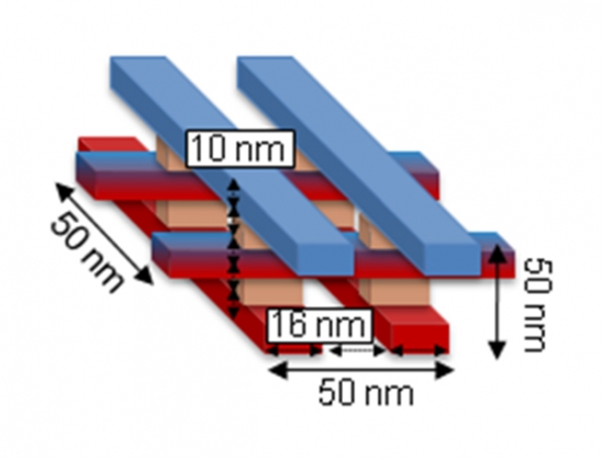
In the spirit of Feynman’s insight, and in response to the challenges he issued as a way to inspire scientific and engineering creativity, electrical and computer engineers at UC Santa Barbara [University of California at Santa Barbara, UCSB] have developed a design for a functional nanoscale computing device. The concept involves a dense, three-dimensional circuit operating on an unconventional type of logic that could, theoretically, be packed into a block no bigger than 50 nanometers on any side.

A figure depicting the structure of stacked memristors with dimensions that could satisfy the Feynman Grand Challenge Photo Credit: Courtesy Image

A figure depicting the structure of stacked memristors with dimensions that could satisfy the Feynman Grand Challenge. Photo Credit: Courtesy Image

An Oct. 27, 2016 UCSB news release (also on EurekAlert) by Sonia Fernandez, which originated the news item, offers a basic explanation of the work (useful for anyone unfamiliar with memristors) along with more detail,

“Novel computing paradigms are needed to keep up with the demand for faster, smaller and more energy-efficient devices,” said Gina Adam, postdoctoral researcher at UCSB’s Department of Computer Science and lead author of the paper “Optimized stateful material implication logic for three dimensional data manipulation,” published in the journal Nano Research. “In a regular computer, data processing and memory storage are separated, which slows down computation. Processing data directly inside a three-dimensional memory structure would allow more data to be stored and processed much faster.”

While efforts to shrink computing devices have been ongoing for decades — in fact, Feynman’s challenges as he presented them in his 1959 talk have been met — scientists and engineers continue to carve out room at the bottom for even more advanced nanotechnology. A nanoscale 8-bit adder operating in 50-by-50-by-50 nanometer dimension, put forth as part of the current Feynman Grand Prize challenge by the Foresight Institute, has not yet been achieved. However, the continuing development and fabrication of progressively smaller components is bringing this virus-sized computing device closer to reality, said Dmitri Strukov, a UCSB professor of computer science.

“Our contribution is that we improved the specific features of that logic and designed it so it could be built in three dimensions,” he said.

Key to this development is the use of a logic system called material implication logic combined with memristors — circuit elements whose resistance depends on the most recent charges and the directions of those currents that have flowed through them. Unlike the conventional computing logic and circuitry found in our present computers and other devices, in this form of computing, logic operation and information storage happen simultaneously and locally. This greatly reduces the need for components and space typically used to perform logic operations and to move data back and forth between operation and memory storage. The result of the computation is immediately stored in a memory element, which prevents data loss in the event of power outages — a critical function in autonomous systems such as robotics.

In addition, the researchers reconfigured the traditionally two-dimensional architecture of the memristor into a three-dimensional block, which could then be stacked and packed into the space required to meet the Feynman Grand Prize Challenge.

“Previous groups show that individual blocks can be scaled to very small dimensions, let’s say 10-by-10 nanometers,” said Strukov, who worked at technology company Hewlett-Packard’s labs when they ramped up development of memristors and material implication logic. By applying those results to his group’s developments, he said, the challenge could easily be met.

The tiny memristors are being heavily researched in academia and in industry for their promising uses in memory storage and neuromorphic computing. While implementations of material implication logic are rather exotic and not yet mainstream, uses for it could pop up any time, particularly in energy scarce systems such as robotics and medical implants.

“Since this technology is still new, more research is needed to increase its reliability and lifetime and to demonstrate large scale three-dimensional circuits tightly packed in tens or hundreds of layers,” Adam said.

HP Labs, mentioned in the news release, announced the ‘discovery’ of memristors and subsequent application of engineering control in two papers in 2008.

Here’s a link to and a citation for the UCSB paper,

Optimized stateful material implication logic for threedimensional data manipulation by Gina C. Adam, Brian D. Hoskins, Mirko Prezioso, &Dmitri B. Strukov. Nano Res. (2016) pp. 1 – 10. doi:10.1007/s12274-016-1260-1 First Online: 29 September 2016

This paper is behind a paywall.

You can find many articles about memristors here by using either ‘memristor’ or ‘memristors’ as your search term.

Ocean-inspired coatings for organic electronics

An Oct. 19, 2016 news item on phys.org describes the advantages a new coating offers and the specific source of inspiration,

In a development beneficial for both industry and environment, UC Santa Barbara [University of California at Santa Barbara] researchers have created a high-quality coating for organic electronics that promises to decrease processing time as well as energy requirements.

“It’s faster, and it’s nontoxic,” said Kollbe Ahn, a research faculty member at UCSB’s Marine Science Institute and corresponding author of a paper published in Nano Letters.

In the manufacture of polymer (also known as “organic”) electronics—the technology behind flexible displays and solar cells—the material used to direct and move current is of supreme importance. Since defects reduce efficiency and functionality, special attention must be paid to quality, even down to the molecular level.

Often that can mean long processing times, or relatively inefficient processes. It can also mean the use of toxic substances. Alternatively, manufacturers can choose to speed up the process, which could cost energy or quality.

Fortunately, as it turns out, efficiency, performance and sustainability don’t always have to be traded against each other in the manufacture of these electronics. Looking no further than the campus beach, the UCSB researchers have found inspiration in the mollusks that live there. Mussels, which have perfected the art of clinging to virtually any surface in the intertidal zone, serve as the model for a molecularly smooth, self-assembled monolayer for high-mobility polymer field-effect transistors—in essence, a surface coating that can be used in the manufacture and processing of the conductive polymer that maintains its efficiency.

An Oct. 18, 2016 UCSB news release by Sonia Fernandez, which originated the news item, provides greater technical detail,

More specifically, according to Ahn, it was the mussel’s adhesion mechanism that stirred the researchers’ interest. “We’re inspired by the proteins at the interface between the plaque and substrate,” he said.

Before mussels attach themselves to the surfaces of rocks, pilings or other structures found in the inhospitable intertidal zone, they secrete proteins through the ventral grove of their feet, in an incremental fashion. In a step that enhances bonding performance, a thin priming layer of protein molecules is first generated as a bridge between the substrate and other adhesive proteins in the plaques that tip the byssus threads of their feet to overcome the barrier of water and other impurities.

That type of zwitterionic molecule — with both positive and negative charges — inspired by the mussel’s native proteins (polyampholytes), can self-assemble and form a sub-nano thin layer in water at ambient temperature in a few seconds. The defect-free monolayer provides a platform for conductive polymers in the appropriate direction on various dielectric surfaces.

Current methods to treat silicon surfaces (the most common dielectric surface), for the production of organic field-effect transistors, requires a batch processing method that is relatively impractical, said Ahn. Although heat can hasten this step, it involves the use of energy and increases the risk of defects.

With this bio-inspired coating mechanism, a continuous roll-to-roll dip coating method of producing organic electronic devices is possible, according to the researchers. It also avoids the use of toxic chemicals and their disposal, by replacing them with water.

“The environmental significance of this work is that these new bio-inspired primers allow for nanofabrication on silicone dioxide surfaces in the absence of organic solvents, high reaction temperatures and toxic reagents,” said co-author Roscoe Lindstadt, a graduate student researcher in UCSB chemistry professor Bruce Lipshutz’s lab. “In order for practitioners to switch to newer, more environmentally benign protocols, they need to be competitive with existing ones, and thankfully device performance is improved by using this ‘greener’ method.”

Here’s a link to and a citation for the research paper,

Molecularly Smooth Self-Assembled Monolayer for High-Mobility Organic Field-Effect Transistors by Saurabh Das, Byoung Hoon Lee, Roscoe T. H. Linstadt, Keila Cunha, Youli Li, Yair Kaufman, Zachary A. Levine, Bruce H. Lipshutz, Roberto D. Lins, Joan-Emma Shea, Alan J. Heeger, and B. Kollbe Ahn. Nano Lett., 2016, 16 (10), pp 6709–6715
DOI: 10.1021/acs.nanolett.6b03860 Publication Date (Web): September 27, 2016

Copyright © 2016 American Chemical Society

This paper is behind a paywall but the scientists have made an illustration available,

An artist's concept of a zwitterionic molecule of the type secreted by mussels to prime surfaces for adhesion Photo Credit: Peter Allen

An artist’s concept of a zwitterionic molecule of the type secreted by mussels to prime surfaces for adhesion Photo Credit: Peter Allen

Connecting chaos and entanglement

Researchers seem to have stumbled across a link between classical and quantum physics. A July 12, 2016 University of California at Santa Barbara (UCSB) news release (also on EurekAlert) by Sonia Fernandez provides a description of both classical and quantum physics, as well as, the research that connects the two,

Using a small quantum system consisting of three superconducting qubits, researchers at UC Santa Barbara and Google have uncovered a link between aspects of classical and quantum physics thought to be unrelated: classical chaos and quantum entanglement. Their findings suggest that it would be possible to use controllable quantum systems to investigate certain fundamental aspects of nature.

“It’s kind of surprising because chaos is this totally classical concept — there’s no idea of chaos in a quantum system,” Charles Neill, a researcher in the UCSB Department of Physics and lead author of a paper that appears in Nature Physics. “Similarly, there’s no concept of entanglement within classical systems. And yet it turns out that chaos and entanglement are really very strongly and clearly related.”

Initiated in the 15th century, classical physics generally examines and describes systems larger than atoms and molecules. It consists of hundreds of years’ worth of study including Newton’s laws of motion, electrodynamics, relativity, thermodynamics as well as chaos theory — the field that studies the behavior of highly sensitive and unpredictable systems. One classic example of chaos theory is the weather, in which a relatively small change in one part of the system is enough to foil predictions — and vacation plans — anywhere on the globe.

At smaller size and length scales in nature, however, such as those involving atoms and photons and their behaviors, classical physics falls short. In the early 20th century quantum physics emerged, with its seemingly counterintuitive and sometimes controversial science, including the notions of superposition (the theory that a particle can be located in several places at once) and entanglement (particles that are deeply linked behave as such despite physical distance from one another).

And so began the continuing search for connections between the two fields.

All systems are fundamentally quantum systems, according [to] Neill, but the means of describing in a quantum sense the chaotic behavior of, say, air molecules in an evacuated room, remains limited.

Imagine taking a balloon full of air molecules, somehow tagging them so you could see them and then releasing them into a room with no air molecules, noted co-author and UCSB/Google researcher Pedram Roushan. One possible outcome is that the air molecules remain clumped together in a little cloud following the same trajectory around the room. And yet, he continued, as we can probably intuit, the molecules will more likely take off in a variety of velocities and directions, bouncing off walls and interacting with each other, resting after the room is sufficiently saturated with them.

“The underlying physics is chaos, essentially,” he said. The molecules coming to rest — at least on the macroscopic level — is the result of thermalization, or of reaching equilibrium after they have achieved uniform saturation within the system. But in the infinitesimal world of quantum physics, there is still little to describe that behavior. The mathematics of quantum mechanics, Roushan said, do not allow for the chaos described by Newtonian laws of motion.

To investigate, the researchers devised an experiment using three quantum bits, the basic computational units of the quantum computer. Unlike classical computer bits, which utilize a binary system of two possible states (e.g., zero/one), a qubit can also use a superposition of both states (zero and one) as a single state. Additionally, multiple qubits can entangle, or link so closely that their measurements will automatically correlate. By manipulating these qubits with electronic pulses, Neill caused them to interact, rotate and evolve in the quantum analog of a highly sensitive classical system.

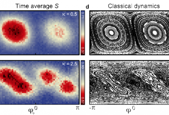
The result is a map of entanglement entropy of a qubit that, over time, comes to strongly resemble that of classical dynamics — the regions of entanglement in the quantum map resemble the regions of chaos on the classical map. The islands of low entanglement in the quantum map are located in the places of low chaos on the classical map.

“There’s a very clear connection between entanglement and chaos in these two pictures,” said Neill. “And, it turns out that thermalization is the thing that connects chaos and entanglement. It turns out that they are actually the driving forces behind thermalization.

“What we realize is that in almost any quantum system, including on quantum computers, if you just let it evolve and you start to study what happens as a function of time, it’s going to thermalize,” added Neill, referring to the quantum-level equilibration. “And this really ties together the intuition between classical thermalization and chaos and how it occurs in quantum systems that entangle.”

The study’s findings have fundamental implications for quantum computing. At the level of three qubits, the computation is relatively simple, said Roushan, but as researchers push to build increasingly sophisticated and powerful quantum computers that incorporate more qubits to study highly complex problems that are beyond the ability of classical computing — such as those in the realms of machine learning, artificial intelligence, fluid dynamics or chemistry — a quantum processor optimized for such calculations will be a very powerful tool.

“It means we can study things that are completely impossible to study right now, once we get to bigger systems,” said Neill.

Experimental link between quantum entanglement (left) and classical chaos (right) found using a small quantum computer. Photo Credit: Courtesy Image (Courtesy: UCSB)

Experimental link between quantum entanglement (left) and classical chaos (right) found using a small quantum computer. Photo Credit: Courtesy Image (Courtesy: UCSB)

Here’s a link to and a citation for the paper,

Ergodic dynamics and thermalization in an isolated quantum system by C. Neill, P. Roushan, M. Fang, Y. Chen, M. Kolodrubetz, Z. Chen, A. Megrant, R. Barends, B. Campbell, B. Chiaro, A. Dunsworth, E. Jeffrey, J. Kelly, J. Mutus, P. J. J. O’Malley, C. Quintana, D. Sank, A. Vainsencher, J. Wenner, T. C. White, A. Polkovnikov, & J. M. Martinis. Nature Physics (2016)  doi:10.1038/nphys3830 Published online 11 July 2016

This paper is behind a paywall.

The challenges of wet adhesion and how nature solves the problem

I usually post about dry adhesion, that is, sticking to dry surfaces in the way a gecko might. This particular piece concerns wet adhesion, a matter of particular interest in medicine where you want bandages and such to stick to a wet surface and in marine circles where they want barnacles and such to stop adhering to boat and ship hulls.

An Aug. 6, 2015 news item on ScienceDaily touts ‘wet adhesion’ research focused on medicinal matters,

Wet adhesion is a true engineering challenge. Marine animals such as mussels, oysters and barnacles are naturally equipped with the means to adhere to rock, buoys and other underwater structures and remain in place no matter how strong the waves and currents.

Synthetic wet adhesive materials, on the other hand, are a different story.

Taking their cue from Mother Nature and the chemical composition of mussel foot proteins, the Alison Butler Lab at UC [University of California] Santa Barbara [UCSB] decided to improve a small molecule called the siderophore cyclic trichrysobactin (CTC) that they had previously discovered. They modified the molecule and then tested its adhesive strength in aqueous environments. The result: a compound that rivals the staying power of mussel glue.

An Aug. 6, 2015 UCSB news release by Julie Cohen, which originated the news item, describes some of the reasons for the research, the interdisciplinary aspect of the collaboration, and technical details of the work (Note: Links have been removed),

“There’s real need in a lot of environments, including medicine, to be able to have glues that would work in an aqueous environment,” said co-author Butler, a professor in UCSB’s Department of Chemistry and Biochemistry. “So now we have the basis of what we might try to develop from here.”

Also part of the interdisciplinary effort were Jacob Israelachvili’s Interfacial Sciences Lab in UCSB’s Department of Chemical Engineering and J. Herbert Waite, a professor in the Department of Molecular, Cellular and Developmental Biology, whose own work focuses on wet adhesion.

“We just happened to see a visual similarity between compounds in the siderophore CTC and in mussel foot proteins,” Butler explained. Siderophores are molecules that bind and transport iron in microorganisms such as bacteria. “We specifically looked at the synergy between the role of the amino acid lysine and catechol,” she added. “Both are present in mussel foot proteins and in CTC.”
Mussel foot proteins contain similar amounts of lysine and the catechol dopa. Catechols are chemical compounds used in such biological functions as neurotransmission. However, certain proteins have adopted dopa for adhesive purposes.

From discussions with Waite, Butler realized that CTC contained not only lysine but also a compound similar to dopa. Further, CTC paired its catechol with lysine, just like mussel foot proteins do.

“We developed a better, more stable molecule than the actual CTC,” Butler explained. “Then we modified it to tease out the importance of the contributions from either lysine or the catechol.”

Co-lead author Greg Maier, a graduate student in the Butler Lab, created six different compounds with varying amounts of lysine and catechol. The Israelachvili lab tested each compound for its surface and adhesion characteristics. Co-lead author Michael Rapp used a surface force apparatus developed in the lab to measure the interactions between mica surfaces in a saline solution.

Only the two compounds containing a cationic amine, such as lysine, and catechol exhibited adhesive strength and a reduced intervening film thickness, which measures the amount two surfaces can be squeezed together. Compounds without catechol had greatly diminished adhesion levels but a similarly reduced film thickness. Without lysine, the compounds displayed neither characteristic. “Our tests showed that lysine was key, helping to remove salt ions from the surface to allow the glue to get to the underlying surface,” Maier said.

“By looking at a different biosystem that has similar characteristics to some of the best-performing mussel glues, we were able to deduce that these two small components work together synergistically to create a favorable environment at surfaces to promote adherence,” explained Rapp, a chemical engineering graduate student. “Our results demonstrate that these two molecular groups not only prime the surface but also work collectively to build better adhesives that stick to surfaces.”

“In a nutshell, our discovery is that you need lysine and you need the catechol,” Butler concluded. “There’s a one-two punch: the lysine clears and primes the surface and the catechol comes down and hydrogen bonds to the mica surface. This is an unprecedented insight about what needs to happen during wet adhesion.”

Here’s a link to and a citation for the paper,

Adaptive synergy between catechol and lysine promotes wet adhesion by surface salt displacement by Greg P. Maier, Michael V. Rapp, J. Herbert Waite, Jacob N. Israelachvili, and Alison Butler. Science 7 August 2015: Vol. 349 no. 6248 pp. 628-632 DOI: 10.1126/science.aab055

This paper is behind a paywall.

I have previously written about mussels and wet adhesion in a Dec. 13, 2012 posting regarding some research at the University of British Columbia (Canada). As for dry adhesion, there’s my June 11, 2014 posting titled: Climb like a gecko (in DARPA’s [US Defense Advanced Research Projects Agency] Z-Man program) amongst others.

Memristor, memristor, you are popular

Regular readers know I have a long-standing interest in memristor and artificial brains. I have three memristor-related pieces of research,  published in the last month or so, for this post.

First, there’s some research into nano memory at RMIT University, Australia, and the University of California at Santa Barbara (UC Santa Barbara). From a May 12, 2015 news item on ScienceDaily,

RMIT University researchers have mimicked the way the human brain processes information with the development of an electronic long-term memory cell.

Researchers at the MicroNano Research Facility (MNRF) have built the one of the world’s first electronic multi-state memory cell which mirrors the brain’s ability to simultaneously process and store multiple strands of information.

The development brings them closer to imitating key electronic aspects of the human brain — a vital step towards creating a bionic brain — which could help unlock successful treatments for common neurological conditions such as Alzheimer’s and Parkinson’s diseases.

A May 11, 2015 RMIT University news release, which originated the news item, reveals more about the researchers’ excitement and about the research,

“This is the closest we have come to creating a brain-like system with memory that learns and stores analog information and is quick at retrieving this stored information,” Dr Sharath said.

“The human brain is an extremely complex analog computer… its evolution is based on its previous experiences, and up until now this functionality has not been able to be adequately reproduced with digital technology.”

The ability to create highly dense and ultra-fast analog memory cells paves the way for imitating highly sophisticated biological neural networks, he said.

The research builds on RMIT’s previous discovery where ultra-fast nano-scale memories were developed using a functional oxide material in the form of an ultra-thin film – 10,000 times thinner than a human hair.

Dr Hussein Nili, lead author of the study, said: “This new discovery is significant as it allows the multi-state cell to store and process information in the very same way that the brain does.

“Think of an old camera which could only take pictures in black and white. The same analogy applies here, rather than just black and white memories we now have memories in full color with shade, light and texture, it is a major step.”

While these new devices are able to store much more information than conventional digital memories (which store just 0s and 1s), it is their brain-like ability to remember and retain previous information that is exciting.

“We have now introduced controlled faults or defects in the oxide material along with the addition of metallic atoms, which unleashes the full potential of the ‘memristive’ effect – where the memory element’s behaviour is dependent on its past experiences,” Dr Nili said.

Nano-scale memories are precursors to the storage components of the complex artificial intelligence network needed to develop a bionic brain.

Dr Nili said the research had myriad practical applications including the potential for scientists to replicate the human brain outside of the body.

“If you could replicate a brain outside the body, it would minimise ethical issues involved in treating and experimenting on the brain which can lead to better understanding of neurological conditions,” Dr Nili said.

The research, supported by the Australian Research Council, was conducted in collaboration with the University of California Santa Barbara.

Here’s a link to and a citation for this memristive nano device,

Donor-Induced Performance Tuning of Amorphous SrTiO3 Memristive Nanodevices: Multistate Resistive Switching and Mechanical Tunability by  Hussein Nili, Sumeet Walia, Ahmad Esmaielzadeh Kandjani, Rajesh Ramanathan, Philipp Gutruf, Taimur Ahmed, Sivacarendran Balendhran, Vipul Bansal, Dmitri B. Strukov, Omid Kavehei, Madhu Bhaskaran, and Sharath Sriram. Advanced Functional Materials DOI: 10.1002/adfm.201501019 Article first published online: 14 APR 2015

© 2015 WILEY-VCH Verlag GmbH & Co. KGaA, Weinheim

This paper is behind a paywall.

The second published piece of memristor-related research comes from a UC Santa Barbara and  Stony Brook University (New York state) team but is being publicized by UC Santa Barbara. From a May 11, 2015 news item on Nanowerk (Note: A link has been removed),

In what marks a significant step forward for artificial intelligence, researchers at UC Santa Barbara have demonstrated the functionality of a simple artificial neural circuit (Nature, “Training and operation of an integrated neuromorphic network based on metal-oxide memristors”). For the first time, a circuit of about 100 artificial synapses was proved to perform a simple version of a typical human task: image classification.

A May 11, 2015 UC Santa Barbara news release (also on EurekAlert)by Sonia Fernandez, which originated the news item, situates this development within the ‘artificial brain’ effort while describing it in more detail (Note: A link has been removed),

“It’s a small, but important step,” said Dmitri Strukov, a professor of electrical and computer engineering. With time and further progress, the circuitry may eventually be expanded and scaled to approach something like the human brain’s, which has 1015 (one quadrillion) synaptic connections.

For all its errors and potential for faultiness, the human brain remains a model of computational power and efficiency for engineers like Strukov and his colleagues, Mirko Prezioso, Farnood Merrikh-Bayat, Brian Hoskins and Gina Adam. That’s because the brain can accomplish certain functions in a fraction of a second what computers would require far more time and energy to perform.

… As you read this, your brain is making countless split-second decisions about the letters and symbols you see, classifying their shapes and relative positions to each other and deriving different levels of meaning through many channels of context, in as little time as it takes you to scan over this print. Change the font, or even the orientation of the letters, and it’s likely you would still be able to read this and derive the same meaning.

In the researchers’ demonstration, the circuit implementing the rudimentary artificial neural network was able to successfully classify three letters (“z”, “v” and “n”) by their images, each letter stylized in different ways or saturated with “noise”. In a process similar to how we humans pick our friends out from a crowd, or find the right key from a ring of similar keys, the simple neural circuitry was able to correctly classify the simple images.

“While the circuit was very small compared to practical networks, it is big enough to prove the concept of practicality,” said Merrikh-Bayat. According to Gina Adam, as interest grows in the technology, so will research momentum.

“And, as more solutions to the technological challenges are proposed the technology will be able to make it to the market sooner,” she said.

Key to this technology is the memristor (a combination of “memory” and “resistor”), an electronic component whose resistance changes depending on the direction of the flow of the electrical charge. Unlike conventional transistors, which rely on the drift and diffusion of electrons and their holes through semiconducting material, memristor operation is based on ionic movement, similar to the way human neural cells generate neural electrical signals.

“The memory state is stored as a specific concentration profile of defects that can be moved back and forth within the memristor,” said Strukov. The ionic memory mechanism brings several advantages over purely electron-based memories, which makes it very attractive for artificial neural network implementation, he added.

“For example, many different configurations of ionic profiles result in a continuum of memory states and hence analog memory functionality,” he said. “Ions are also much heavier than electrons and do not tunnel easily, which permits aggressive scaling of memristors without sacrificing analog properties.”

This is where analog memory trumps digital memory: In order to create the same human brain-type functionality with conventional technology, the resulting device would have to be enormous — loaded with multitudes of transistors that would require far more energy.

“Classical computers will always find an ineluctable limit to efficient brain-like computation in their very architecture,” said lead researcher Prezioso. “This memristor-based technology relies on a completely different way inspired by biological brain to carry on computation.”

To be able to approach functionality of the human brain, however, many more memristors would be required to build more complex neural networks to do the same kinds of things we can do with barely any effort and energy, such as identify different versions of the same thing or infer the presence or identity of an object not based on the object itself but on other things in a scene.

Potential applications already exist for this emerging technology, such as medical imaging, the improvement of navigation systems or even for searches based on images rather than on text. The energy-efficient compact circuitry the researchers are striving to create would also go a long way toward creating the kind of high-performance computers and memory storage devices users will continue to seek long after the proliferation of digital transistors predicted by Moore’s Law becomes too unwieldy for conventional electronics.

Here’s a link to and a citation for the paper,

Training and operation of an integrated neuromorphic network based on metal-oxide memristors by M. Prezioso, F. Merrikh-Bayat, B. D. Hoskins, G. C. Adam, K. K. Likharev,    & D. B. Strukov. Nature 521, 61–64 (07 May 2015) doi:10.1038/nature14441

This paper is behind a paywall but a free preview is available through ReadCube Access.

The third and last piece of research, which is from Rice University, hasn’t received any publicity yet, unusual given Rice’s very active communications/media department. Here’s a link to and a citation for their memristor paper,

2D materials: Memristor goes two-dimensional by Jiangtan Yuan & Jun Lou. Nature Nanotechnology 10, 389–390 (2015) doi:10.1038/nnano.2015.94 Published online 07 May 2015

This paper is behind a paywall but a free preview is available through ReadCube Access.

Dexter Johnson has written up the RMIT research (his May 14, 2015 post on the Nanoclast blog on the IEEE [Institute of Electrical and Electronics Engineers] website). He linked it to research from Mark Hersam’s team at Northwestern University (my April 10, 2015 posting) on creating a three-terminal memristor enabling its use in complex electronics systems. Dexter strongly hints in his headline that these developments could lead to bionic brains.

For those who’d like more memristor information, this June 26, 2014 posting which brings together some developments at the University of Michigan and information about developments in the industrial sector is my suggestion for a starting point. Also, you may want to check out my material on HP Labs, especially prominent in the story due to the company’s 2008 ‘discovery’ of the memristor, described on a page in my Nanotech Mysteries wiki, and the controversy triggered by the company’s terminology (there’s more about the controversy in my April 7, 2010 interview with Forrest H Bennett III).

13,000 year old nanodiamonds and a scientific controversy about extinction

It took scientists from several countries and institutions seven years to reply to criticism of their 2007 theory which posited that a comet exploded over the earth’s surface roughly 13,000 years ago causing mass extinctions and leaving nano-sized diamonds in a layer of the earth’s crust. From a Sept. 1, 2014 news item on Azonano,

Tiny diamonds invisible to human eyes but confirmed by a powerful microscope at the University of Oregon are shining new light on the idea proposed in 2007 that a cosmic event — an exploding comet above North America — sparked catastrophic climate change 12,800 years ago.

In a paper appearing online ahead of print in the Journal of Geology, scientists from 21 universities in six countries report the definitive presence of nanodiamonds at some 32 sites in 11 countries on three continents in layers of darkened soil at the Earth’s Younger Dryas boundary.

The scientists have provided a map showing the areas with nanodiamonds,

The solid line defines the current known limits of the Younger Dryas Boundary field of cosmic-impact proxies, spanning 50 million square kilometers. [downloaded from http://www.news.ucsb.edu/2014/014368/nanodiamonds-are-forever#sthash.FtKG6WwS.dpuf]

The solid line defines the current known limits of the Younger Dryas Boundary field of cosmic-impact proxies, spanning 50 million square kilometers. [downloaded from http://www.news.ucsb.edu/2014/014368/nanodiamonds-are-forever#sthash.FtKG6WwS.dpuf]

 An Aug. 28,, 2014 University of Oregon news release, which originated the Azonano news item, describes the findings and the controversy,

The boundary layer is widespread, the researchers found. The miniscule diamonds, which often form during large impact events, are abundant along with cosmic impact spherules, high-temperature melt-glass, fullerenes, grape-like clusters of soot, charcoal, carbon spherules, glasslike carbon, heium-3, iridium, osmium, platinum, nickel and cobalt.

The combination of components is similar to that found in soils connected with the 1908 in-air explosion of a comet over Siberia and those found in the Cretaceous-Tertiary Boundary (KTB) layer that formed 65 million years ago when a comet or asteroid struck off Mexico and wiped out dinosaurs worldwide.

In the Oct. 9, 2007, issue of Proceedings of the National Academy of Sciences, a 26-member team from 16 institutions proposed that a cosmic impact event set off a 1,300-year-long cold spell known as the Younger Dryas. Prehistoric Clovis culture was fragmented, and widespread extinctions occurred across North America. Former UO researcher Douglas Kennett, a co-author of the new paper and now at Pennsylvania State University, was a member of the original study.

In that [2007] paper and in a series of subsequent studies, reports of nanodiamond-rich soils were documented at numerous sites. However, numerous critics refuted the findings, holding to a long-running theory that over-hunting sparked the extinctions and that the suspected nanodiamonds had been formed by wildfires, volcanism or occasional meteoritic debris, rather than a cosmic event.

The University of Oregon news release goes on to provide a rejoinder from a co-author of both the 2007 paper and the 2014 paper. as well as. a discussion of how the scientists gathered their evidence,

The glassy and metallic materials in the YDB layers would have formed at temperatures in excess of 2,200 degrees Celsius and could not have resulted from the alternative scenarios, said co-author James Kennett, professor emeritus at the University of California, Santa Barbara, in a news release. He also was on the team that originally proposed a comet-based event.

In the new paper, researchers slightly revised the date of the theorized cosmic event and cited six examples of independent research that have found consistent peaks in the creation of the nanodiamonds that match their hypothesis.

“The evidence presented in this paper rejects the alternate hypotheses and settles the debate about the existence of the nanodiamonds,” said the paper’s corresponding author Allen West of GeoScience Consulting of Dewey, Arizona. “We provide the first comprehensive review of the state of the debate and about YDB nanodiamonds deposited across three continents.”

West worked in close consultation with researchers at the various labs that conducted the independent testing, including with co-author Joshua J. Razink, operator and instrument manager since 2011 of the UO’s state-of-the-art high-resolution transmission electron microscope (HR-TEM) in the Center for Advanced Materials Characterization in Oregon (CAMCOR).

Razink was provided with samples previously cited in many of the earlier studies, as well as untested soil samples delivered from multiple new sites. The samples were placed onto grids and analyzed thoroughly, he said.

“These diamonds are incredibly small, on the order of a few nanometers and are invisible to the human eye and even to an optical microscope,” Razink said. “For reference, if you took a meter stick and cut it into one billion pieces, each of those pieces is one nanometer. The only way to really get definitive characterization that these are diamonds is to use tools like the transmission electron microscope. It helps us to rule out that the samples are not graphene or copper. Our findings say these samples are nanodiamonds.”

In addition to the HR-TEM done at the UO, researchers also used standard TEM, electron energy loss spectroscopy (EELS), energy-dispersive X-ray spectroscopy (EDS), selected area diffraction (SAD), fast Fourier transform (FFT) algorithms, and energy-filtered transmission electron microscopy (EFTEM).

“The chemical processing methods described in the paper,” Razink said, “lay out with great detail the methodology that one needs to go through in order to prepare their samples and identify these diamonds.”

The University of California at Santa Barbara (UCSB) produced an Aug. 28, 2014 news release about this work and while there is repetition, there is additional information such as a lede describing some of what was made extinct,

Most of North America’s megafauna — mastodons, short-faced bears, giant ground sloths, saber-toothed cats and American camels and horses — disappeared close to 13,000 years ago at the end of the Pleistocene period. …

An Aug. 27, 2014 news item (scroll down to the end) on ScienceDaily provides a link and a citation to the latest paper.

Disassembling silver nanoparticles

The notion of self-assembling material is a longstanding trope in the nanotechnology narrative. Scientists at the University of California at Santa Barbara (UCSB) have upended this trope with their work on disassembling the silver nanoparticles being used as a method of delivery for medications. From a June 9, 2014 news item on Azonano,

Scientists at UC Santa Barbara have designed a nanoparticle that has a couple of unique — and important — properties. Spherical in shape and silver in composition, it is encased in a shell coated with a peptide that enables it to target tumor cells. What’s more, the shell is etchable so those nanoparticles that don’t hit their target can be broken down and eliminated. The research findings appear today in the journal Nature Materials.

A june 8, 2014 UCSB news release (also on EurekAlert) by Julie Cohen, which originated the news item, explains the technology and this platform’s unique features in more detail,

The core of the nanoparticle employs a phenomenon called plasmonics. In plasmonics, nanostructured metals such as gold and silver resonate in light and concentrate the electromagnetic field near the surface. In this way, fluorescent dyes are enhanced, appearing about tenfold brighter than their natural state when no metal is present. When the core is etched, the enhancement goes away and the particle becomes dim.

UCSB’s Ruoslahti Research Laboratory also developed a simple etching technique using biocompatible chemicals to rapidly disassemble and remove the silver nanoparticles outside living cells. This method leaves only the intact nanoparticles for imaging or quantification, thus revealing which cells have been targeted and how much each cell internalized.

“The disassembly is an interesting concept for creating drugs that respond to a certain stimulus,” said Gary Braun, a postdoctoral associate in the Ruoslahti Lab in the Department of Molecular, Cellular and Developmental Biology (MCDB) and at Sanford-Burnham Medical Research Institute. “It also minimizes the off-target toxicity by breaking down the excess nanoparticles so they can then be cleared through the kidneys.”

This method for removing nanoparticles unable to penetrate target cells is unique. “By focusing on the nanoparticles that actually got into cells,” Braun said, “we can then understand which cells were targeted and study the tissue transport pathways in more detail.”

Some drugs are able to pass through the cell membrane on their own, but many drugs, especially RNA and DNA genetic drugs, are charged molecules that are blocked by the membrane. These drugs must be taken in through endocytosis, the process by which cells absorb molecules by engulfing them.

“This typically requires a nanoparticle carrier to protect the drug and carry it into the cell,” Braun said. “And that’s what we measured: the internalization of a carrier via endocytosis.”

Because the nanoparticle has a core shell structure, the researchers can vary its exterior coating and compare the efficiency of tumor targeting and internalization. Switching out the surface agent enables the targeting of different diseases — or organisms in the case of bacteria — through the use of different target receptors. According to Braun, this should turn into a way to optimize drug delivery where the core is a drug-containing vehicle.

“These new nanoparticles have some remarkable properties that have already proven useful as a tool in our work that relates to targeted drug delivery into tumors,” said Erkki Ruoslahti, adjunct distinguished professor in UCSB’s Center for Nanomedicine and MCDB department and at Sanford-Burnham Medical Research Institute. “They also have potential applications in combating infections. Dangerous infections caused by bacteria that are resistant to all antibiotics are getting more common, and new approaches to deal with this problem are desperately needed. Silver is a locally used antibacterial agent and our targeting technology may make it possible to use silver nanoparticles in treating infections anywhere in the body.”

Here’s a link to and a citation for the paper,

Etchable plasmonic nanoparticle probes to image and quantify cellular internalization by Gary B. Braun, Tomas Friman, Hong-Bo Pang, Alessia Pallaoro, Tatiana Hurtado de Mendoza, Anne-Mari A. Willmore, Venkata Ramana Kotamraju, Aman P. Mann, Zhi-Gang She, Kazuki N. Sugahara, Norbert O. Reich, Tambet Teesalu, & Erkki Ruoslahti. Nature Materials (2014) doi:10.1038/nmat3982 Published online 08 June 2014

This article is behind a paywall but there is a free preview via ReadCube Access.

Competition, collaboration, and a smaller budget: the US nano community responds

Before getting to the competition, collaboration, and budget mentioned in the head for this posting, I’m supplying some background information.

Within the context of a May 20, 2014 ‘National Nanotechnology Initiative’ hearing before the U.S. House of Representatives Subcommittee on Research and Technology, Committee on Science, Space, and Technology, the US General Accountability Office (GAO) presented a 22 pp. précis (PDF; titled: NANOMANUFACTURING AND U.S. COMPETITIVENESS; Challenges and Opportunities) of its 125 pp. (PDF version report titled: Nanomanufacturing: Emergence and Implications for U.S. Competitiveness, the Environment, and Human Health).

Having already commented on the full report itself in a Feb. 10, 2014 posting, I’m pointing you to Dexter Johnson’s May 21, 2014 post on his Nanoclast blog (on the IEEE [Institute of Electrical and Electronics Engineers] website) where he discusses the précis from the perspective of someone who was consulted by the US GAO when they were writing the full report (Note: Links have been removed),

I was interviewed extensively by two GAO economists for the accompanying [full] report “Nanomanufacturing: Emergence and Implications for U.S. Competitiveness, the Environment, and Human Health,” where I shared background information on research I helped compile and write on global government funding of nanotechnology.

While I acknowledge that the experts who were consulted for this report are more likely the source for its views than I am, I was pleased to see the report reflect many of my own opinions. Most notable among these is bridging the funding gap in the middle stages of the manufacturing-innovation process, which is placed at the top of the report’s list of challenges.

While I am in agreement with much of the report’s findings, it suffers from a fundamental misconception in seeing nanotechnology’s development as a kind of race between countries. [emphases mine]

(I encourage you to read the full text of Dexter’s comments as he offers more than a simple comment about competition.)

Carrying on from this notion of a ‘nanotechnology race’, at least one publication focused on that aspect. From the May 20, 2014 article by Ryan Abbott for CourthouseNews.com,

Nanotech Could Keep U.S. Ahead of China

WASHINGTON (CN) – Four of the nation’s leading nanotechnology scientists told a U.S. House of Representatives panel Tuesday that a little tweaking could go a long way in keeping the United States ahead of China and others in the industry.

The hearing focused on the status of the National Nanotechnology Initiative, a federal program launched in 2001 for the advancement of nanotechnology.

As I noted earlier, the hearing was focused on the National Nanotechnology Initiative (NNI) and all of its efforts. It’s quite intriguing to see what gets emphasized in media reports and, in this case, the dearth of media reports.

I have one more tidbit, the testimony from Lloyd Whitman, Interim Director of the National Nanotechnology Coordination Office and Deputy Director of the Center for Nanoscale Science and Technology, National Institute of Standards and Technology. The testimony is in a May 21, 2014 news item on insurancenewsnet.com,

Testimony by Lloyd Whitman, Interim Director of the National Nanotechnology Coordination Office and Deputy Director of the Center for Nanoscale Science and Technology, National Institute of Standards and Technology

Chairman Bucshon, Ranking Member Lipinski, and Members of the Committee, it is my distinct privilege to be here with you today to discuss nanotechnology and the role of the National Nanotechnology Initiative in promoting its development for the benefit of the United States.

Highlights of the National Nanotechnology Initiative

Our current Federal research and development program in nanotechnology is strong. The NNI agencies continue to further the NNI’s goals of (1) advancing nanotechnology R&D, (2) fostering nanotechnology commercialization, (3) developing and maintaining the U.S. workforce and infrastructure, and (4) supporting the responsible and safe development of nanotechnology. …

,,,

The sustained, strategic Federal investment in nanotechnology R&D combined with strong private sector investments in the commercialization of nanotechnology-enabled products has made the United States the global leader in nanotechnology. The most recent (2012) NNAP report analyzed a wide variety of sources and metrics and concluded that “… in large part as a result of the NNI the United States is today… the global leader in this exciting and economically promising field of research and technological development.” n10 A recent report on nanomanufacturing by Congress’s own Government Accountability Office (GAO) arrived at a similar conclusion, again drawing on a wide variety of sources and stakeholder inputs. n11 As discussed in the GAO report, nanomanufacturing and commercialization are key to capturing the value of Federal R&D investments for the benefit of the U.S. economy. The United States leads the world by one important measure of commercial activity in nanotechnology: According to one estimate, n12 U.S. companies invested $4.1 billion in nanotechnology R&D in 2012, far more than investments by companies in any other country.  …

There’s cognitive dissonance at work here as Dexter notes in his own way,

… somewhat ironically, the [GAO] report suggests that one of the ways forward is more international cooperation, at least in the development of international standards. And in fact, one of the report’s key sources of information, Mihail Roco, has made it clear that international cooperation in nanotechnology research is the way forward.

It seems to me that much of the testimony and at least some of the anxiety about being left behind can be traced to a decreased 2015 budget allotment for nanotechnology (mentioned here in a March 31, 2014 posting [US National Nanotechnology Initiative’s 2015 budget request shows a decrease of $200M]).

One can also infer a certain anxiety from a recent presentation by Barbara Herr Harthorn, head of UCSB’s [University of California at Santa Barbara) Center for Nanotechnology in Society (CNS). She was at a February 2014 meeting of the Presidential Commission for the Study of Bioethical Issues (mentioned in parts one and two [the more substantive description of the meeting which also features a Canadian academic from the genomics community] of my recent series on “Brains, prostheses, nanotechnology, and human enhancement”). II noted in part five of the series what seems to be a shift towards brain research as a likely beneficiary of the public engagement work accomplished under NNI auspices and, in the case of the Canadian academic, the genomics effort.

The Americans are not the only ones feeling competitive as this tweet from Richard Jones, Pro-Vice Chancellor for Research and Innovation at Sheffield University (UK), physicist, and author of Soft Machines, suggests,

May 18

The UK has fewer than 1% of world patents on graphene, despite it being discovered here, according to the FT –

I recall reading a report a few years back which noted that experts in China were concerned about falling behind internationally in their research efforts. These anxieties are not new, CP Snow’s book and lecture The Two Cultures (1959) also referenced concerns in the UK about scientific progress and being left behind.

Competition/collaboration is an age-old conundrum and about as ancient as anxieties of being left behind. The question now is how are we all going to resolve these issues this time?

ETA May 28, 2014: The American Institute of Physics (AIP) has produced a summary of the May 20, 2014 hearing as part of their FYI: The AIP Bulletin of Science Policy News, May 27, 2014 (no. 93).

ETA Sept. 12, 2014: My first posting about the diminished budget allocation for the US NNI was this March 31, 2014 posting.