Tag Archives: Université du Québec

Canada and some graphene scene tidbits

For a long time It seemed as if every country in the world, except Canada, had some some sort of graphene event. According to a July 16, 2015 news item on Nanotechnology Now, Canada has now stepped up, albeit, in a peculiarly Canadian fashion. First the news,

Mid October [Oct. 14 -16, 2015], the Graphene & 2D Materials Canada 2015 International Conference & Exhibition (www.graphenecanada2015.com) will take place in Montreal (Canada).

I found a July 16, 2015 news release (PDF) announcing the Canadian event on the lead organizer’s (Phantoms Foundation located in Spain) website,

On the second day of the event (15th October, 2015), an Industrial Forum will bring together top industry leaders to discuss recent advances in technology developments and business opportunities in graphene commercialization.
At this stage, the event unveils 38 keynote & invited speakers. On the Industrial Forum 19 of them will present the latest in terms of Energy, Applications, Production and Worldwide Initiatives & Priorities.

Plenary:
Gary Economo (Grafoid Inc., Canada)
Khasha Ghaffarzadeh (IDTechEx, UK)
Shu-Jen Han (IBM T.J. Watson Research Center, USA)
Bor Z. Jang (Angstron Materials, USA)
Seongjun Park (Samsung Advanced Institute of Technology (SAIT), Korea)
Chun-Yun Sung (Lockheed Martin, USA)

Parallel Sessions:
Gordon Chiu (Grafoid Inc., Canada)
Jesus de la Fuente (Graphenea, Spain)
Mark Gallerneault (ALCERECO Inc., Canada)
Ray Gibbs (Haydale Graphene Industries, UK)
Masataka Hasegawa (AIST, Japan)
Byung Hee Hong (SNU & Graphene Square, Korea)
Tony Ling (Jestico + Whiles, UK)
Carla Miner (SDTC, Canada)
Gregory Pognon (THALES Research & Technology, France)
Elena Polyakova (Graphene Laboratories Inc, USA)
Federico Rosei (INRS–EMT, Université du Québec, Canada)
Aiping Yu (University of Waterloo, Canada)
Hua Zhang (MSE-NTU, Singapore)

Apart from the industrial forum, several industry-related activities will be organized:
– Extensive thematic workshops in parallel (Standardization, Materials & Devices Characterization, Bio & Health and Electronic Devices)
– An exhibition carried out with the latest graphene trends (Grafoid, RAYMOR NanoIntegris, Nanomagnetics Instruments, ICEX and Xerox Research Centre of Canada (XRCC) already confirmed)
– B2B meetings to foster technical cooperation in the field of Graphene

It’s still possible to contribute to the event with an oral presentation. The call for abstracts is open until July, 20 [2015]. [emphasis mine]

Graphene Canada 2015 is already supported by Canada’s leading graphene applications developer, Grafoid Inc., Tourisme Montréal and Université de Montréal.

This is what makes the event peculiarly Canadian: multiculturalism, anyone? From the news release,

Organisers: Phantoms Foundation www.phantomsnet.net & Grafoid Foundation (lead organizers)

CEMES/CNRS (France) | Grafoid (Canada) | Catalan Institute of Nanoscience and Nanotechnology – ICN2 (Spain) | IIT (Italy) | McGill University, Canada | Texas Instruments (USA) | Université Catholique de Louvain (Belgium) | Université de Montreal, Canada

It’s billed as a ‘Canada Graphene 2015’ and, as I recall, these types of events don’t usually have so many other countries listed as organizers. For example, UK Graphene 2015 would have mostly or all of its organizers (especially the leads) located in the UK.

Getting to the Canadian content, I wrote about Grafoid at length tracking some of its relationships to companies it owns, a business deal with Hydro Québec, and a partnership with the University of Waterloo, and a nonrepayable grant from the Canadian federal government (Sustainable Development Technology Canada [SDTC]) in a Feb. 23, 2015 posting. Do take a look at the post if you’re curious about the heavily interlinked nature of the Canadian graphene scene and take another look at the list of speakers and their agencies (Mark Gallerneault of ALCERECO [partially owned by Grafoid], Carla Miner of SDTC [Grafoid received monies from the Canadian federal department],  Federico Rosei of INRS–EMT, Université du Québec [another Quebec link], Aiping Yu, University of Waterloo [an academic partner to Grafoid]). The Canadian graphene community is a small one so it’s not surprising there are links between the Canadian speakers but it does seem odd that Lomiko Metals is not represented here. Still, new speakers have been announced since the news release (e.g., Frank Koppens of ICFO, Spain, and Vladimir Falko of Lancaster University, UK) so  time remains.

Meanwhile, Lomiko Metals has announced in a July 17, 2015 news item on Azonano that Graphene 3D labs has changed the percentage of its outstanding shares affecting the percentage that Lomiko owns, amid some production and distribution announcements. The bit about launching commercial sales of its graphene filament seems more interesting to me,

On March 16, 2015 Graphene 3D Lab (TSXV:GGG) (OTCQB:GPHBF) announced that it launched commercial sales of its Conductive Graphene Filament for 3D printing. The filament incorporates highly conductive proprietary nano-carbon materials to enhance the properties of PLA, a widely used thermoplastic material for 3D printing; therefore, the filament is compatible with most commercially available 3D printers. The conductive filament can be used to print conductive traces (similar to as used in circuit boards) within 3D printed parts for electronics.

So, that’s all I’ve got for Canada’s graphene scene.
A multiferroic material for more powerful solar cells

A Nov. 12, 2014 INRS (Institut national de la recherche scientifique; Université du Québec) news release (also on EurekAlert), describes new work on solar cells from Federico Rosei’s laboratory (Note: Links have been removed; A French language version of the news release can be found here),

Applying a thin film of metallic oxide significantly boosts the performance of solar panel cells—as recentlydemonstrated by Professor Federico Rosei and his team at the Énergie Matériaux Télécommunications Research Centre at Institut national de la recherche scientifique (INRS). The researchers have developed a new class of materials comprising elements such as bismuth, iron, chromium, and oxygen. These“multiferroic” materials absorb solar radiation and possess unique electrical and magnetic properties. This makes them highly promising for solar technology, and also potentially useful in devices like electronic sensors and flash memory drives. …

The INRS research team discovered that by changing the conditions under which a thin film of these materials is applied, the wavelengths of light that are absorbed can be controlled. A triple-layer coating of these materials—barely 200 nanometres thick—captures different wavelengths of light. This coating converts much more light into electricity than previous trials conducted with a single layer of the same material. With a conversion efficiency of 8.1% reported by [Riad] Nechache and his coauthors, this is a major breakthrough in the field.

The team currently envisions adding this coating to traditional single-crystal silicon solar cells (currently available on the market). They believe it could increase maximum solar efficiency by 18% to 24% while also boosting cell longevity. As this technology draws on a simplified structure and processes, as well as abundant and stable materials, new photovoltaic (PV) cells will be more powerful and cost less. This means that the INRS team’s breakthrough may make it possible to reposition silicon PV cells at the forefront of the highly competitive solar energy market.

Here’s a link to and a citation for the paper,

Bandgap tuning of multiferroic oxide solar cells by R. Nechache, C. Harnagea, S. Li, L. Cardenas, W. Huang,  J. Chakrabartty, & F. Rosei. Nature Photonics (2014) doi:10.1038/nphoton.2014.255 Published online
10 November 2014

This paper is behind a paywall although there is a free preview via ReadCube Access.

I last mentioned Federico Rose in a March 4, 2014 post about a talk (The exploration of the role of nanoscience in tomorrow’s energy solutions) he was giving in Vancouver (Canada).

McGill University researchers get closer to making organic nanoelectronics a reality

You can’t rush out and buy products with organic nanoelectronic components yet but one day you will and you’ll have Dr. Dmitrii Perepichka at McGill University (Montréal, Canada), Dr. Federico Rosei of the Institut national de la recherche scientifique and the members of their international research team to thank for it. From the McGill University news release,

Although they could revolutionize a wide range of high-tech products such as computer displays or solar cells, organic materials do not have the same ordered chemical composition as inorganic materials, preventing scientists from using them to their full potential. But an international team of researchers led by McGill’s Dr. Dmitrii Perepichka and the Institut national de la recherche scientifique’s Dr. Federico Rosei have published research that shows how to solve this decades-old conundrum. The team has effectively discovered a way to order the molecules in the PEDOT, the single most industrially important conducting polymer.

This is an important step forward for anyone who owns a computer or a mobile phone or anything with transistors. In the 1960s a fellow called Gordon Moore (he went on to co-found Intel) made a prediction (from Intel’s Moore’s Law web page),

Intel co-founder Gordon Moore is a visionary. In 1965, his prediction, popularly known as Moore’s Law, states that the number of transistors on a chip will double about every two years. And Intel has kept that pace for nearly 40 years.

We are almost at the physical limits given our current technologies which is why this new type of organic component is important. Perepichka while noting that there’s still a considerable amount of work to be done before being able to create organic nanoelectronic components speculates about future uses,

By using molecular materials instead of silicon semiconductor, we could one day build transistors that are ten times smaller than what currently exists.” The chips would in fact be only one molecule thick.

The groundbreaking technique used to achieve this capability,

… sounds deceptively simple. The team used an inorganic material – a crystal of copper – as a template. When molecules are dropped onto the crystal, the crystal provokes a chemical reaction and creates a conducting polymer. By using a scanning probe microscope that enabled them to see surfaces with atomic resolution, the researchers discovered that the polymers had imitated the order of the crystal surface. The team is currently only able to produce the reaction in one dimension, i.e. to make a string or line of molecules. The next step will be to add a second dimension in order to make continuous sheets (“organic graphite”) or electronic circuits.

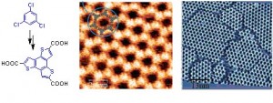
Here are images of the polymer with its chemical composition (at the left),

This image shows the polymers that were created at a resolution of 5 nanometres (the average strand of human hair is 80,000 nanometres wide) Source: Dept. of Chemistry, McGill University

I was interested to note that part of the funding for this project comes from the US Air Force since they also recently funded work on integrating memristors in electronic components (my blog posting here). Here’s my last excerpt from the news release details about the researchers’ affiliations, where the study was published, and the funding sources for the work,

Perepichka is affiliated with McGill University’s department of chemistry and Rosei is affiliated with Institut national de la recherche scientifique – Énergie Matériaux Télécommunications Center, a member of the Université du Québec network. Their research was published online by the Proceedings of the National Academy of Sciences and was funded by the Natural Sciences and Engineering Research Council of Canada, the Air Force Office of Scientific Research and Asian Office of Aerospace Research and Development of the USA, the Petroleum Research Fund of the American Chemical Society, the Fonds québécois de recherche sur la nature et les technologies, and the Ministère du Développement économique, de l’Innovation et de l’Exportation of Quebec.