Researchers at the University of Buffalo (New York state) have created a nanoparticle that can be detected by six imaging devices according to a Jan. 20, 2015 news item on ScienceDaily,
It’s technology so advanced that the machine capable of using it doesn’t yet exist.
Using two biocompatible parts, University at Buffalo researchers and their colleagues have designed a nanoparticle that can be detected by six medical imaging techniques:
• computed tomography (CT) scanning;
• positron emission tomography (PET) scanning;
• photoacoustic imaging;
• fluorescence imaging;
• upconversion imaging; and
• Cerenkov luminescence imaging.
The advantages are obvious should somebody, somewhere create a hexamodal (aka, multimodal, aka hypmodal) sensing device capable of exploiting the advantages of this nanoparticle as the researchers hope.
A Jan. 20, 2015 University of Buffalo news release (also on EurekAlert) by Charlotte Hsu, which originated the news item, describes the ideas underlying the research,
This kind of “hypermodal” imaging — if it came to fruition — would give doctors a much clearer picture of patients’ organs and tissues than a single method alone could provide. It could help medical professionals diagnose disease and identify the boundaries of tumors.
“This nanoparticle may open the door for new ‘hypermodal’ imaging systems that allow a lot of new information to be obtained using just one contrast agent,” says researcher Jonathan Lovell, PhD, UB assistant professor of biomedical engineering. “Once such systems are developed, a patient could theoretically go in for one scan with one machine instead of multiple scans with multiple machines.”
When Lovell and colleagues used the nanoparticles to examine the lymph nodes of mice, they found that CT and PET scans provided the deepest tissue penetration, while the photoacoustic imaging showed blood vessel details that the first two techniques missed.
Differences like these mean doctors can get a much clearer picture of what’s happening inside the body by merging the results of multiple modalities.
A machine capable of performing all six imaging techniques at once has not yet been invented, to Lovell’s knowledge, but he and his coauthors hope that discoveries like theirs will spur development of such technology.
The news release also offers a description of the nanoparticles,
The researchers designed the nanoparticles from two components: An “upconversion” core that glows blue when struck by near-infrared light, and an outer fabric of porphyrin-phospholipids (PoP) that wraps around the core.
Each part has unique characteristics that make it ideal for certain types of imaging.
The core, initially designed for upconversion imaging, is made from sodium, ytterbium, fluorine, yttrium and thulium. The ytterbium is dense in electrons — a property that facilitates detection by CT scans.
The PoP wrapper has biophotonic qualities that make it a great match for fluorescence and photoacoustic imagining. The PoP layer also is adept at attracting copper, which is used in PET and Cerenkov luminescence imaging.
“Combining these two biocompatible components into a single nanoparticle could give tomorrow’s doctors a powerful, new tool for medical imaging,” says Prasad, also a SUNY Distinguished Professor of chemistry, physics, medicine and electrical engineering at UB. “More studies would have to be done to determine whether the nanoparticle is safe to use for such purposes, but it does not contain toxic metals such as cadmium that are known to pose potential risks and found in some other nanoparticles.”
“Another advantage of this core/shell imaging contrast agent is that it could enable biomedical imaging at multiple scales, from single-molecule to cell imaging, as well as from vascular and organ imaging to whole-body bioimaging,” Chen adds. “These broad, potential capabilities are due to a plurality of optical, photoacoustic and radionuclide imaging abilities that the agent possesses.”
Lovell says the next step in the research is to explore additional uses for the technology.
For example, it might be possible to attach a targeting molecule to the PoP surface that would enable cancer cells to take up the particles, something that photoacoustic and fluorescence imaging can detect due to the properties of the smart PoP coating. This would enable doctors to better see where tumors begin and end, Lovell says.
The researchers have provided two images,
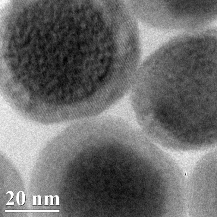
This transmission electron microscopy image shows the nanoparticles, which consist of a core that glows blue when struck by near-infrared light, and an outer fabric of porphyrin-phospholipids (PoP) that wraps around the core.
Credit: Jonathan Lovell
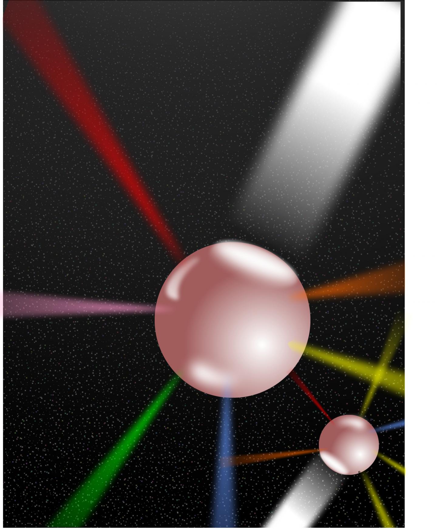
University at Buffalo researchers and colleagues have designed a nanoparticle detectable by six medical imaging techniques. This illustration depicts the particles as they are struck by beams of energy and emit signals that can be detected by the six methods: CT and PET scanning, along with photoacoustic, fluorescence, upconversion and Cerenkov luminescence imaging.
Credit: Jonathan Lovell
Here’s a link to and a citation for the paper,
Hexamodal Imaging with Porphyrin-Phospholipid-Coated Upconversion Nanoparticles by James Rieffel, Feng Chen, Jeesu Kim, Guanying Chen, Wei Shao, Shuai Shao, Upendra Chitgupi, Reinier Hernandez, Stephen A. Graves, Robert J. Nickles, Paras N. Prasad, Chulhong Kim, Weibo Cai, and Jonathan F. Lovell. Advanced Materials DOI: 10.1002/adma.201404739 Article first published online: 14 JAN 2015
© 2015 WILEY-VCH Verlag GmbH & Co. KGaA, Weinheim
This article is behind a paywall.