Tag Archives: University of California at Riverside

Better performing solar cells with newly discovered property of pristine graphene

Light-harvesting devices—I like that better than solar cells or the like but I think that the term serves as a category rather than a name/label for a specific device. Enough musing. A December 17, 2018 news item on Nanowerk describes the latest about graphene and light-harvesting devices (Note: A link has been removed,

An international research team, co-led by a physicist at the University of California, Riverside, has discovered a new mechanism for ultra-efficient charge and energy flow in graphene, opening up opportunities for developing new types of light-harvesting devices.

The researchers fabricated pristine graphene — graphene with no impurities — into different geometric shapes, connecting narrow ribbons and crosses to wide open rectangular regions. They found that when light illuminated constricted areas, such as the region where a narrow ribbon connected two wide regions, they detected a large light-induced current, or photocurrent.

The finding that pristine graphene can very efficiently convert light into electricity could lead to the development of efficient and ultrafast photodetectors — and potentially more efficient solar panels.

A December 14, 2018 University of California at Riverside (UCR) news release by Iqbal Pittalwala (also on EurekAlert but published Dec. 17, 2018), which originated the news item,gives a brief description of graphene while adding context for this research,


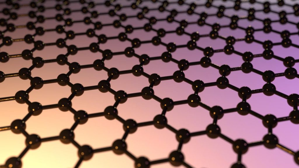
Graphene, a 1-atom thick sheet of carbon atoms arranged in a hexagonal lattice, has many desirable material properties, such as high current-carrying capacity and thermal conductivity. In principle, graphene can absorb light at any frequency, making it ideal material for infrared and other types of photodetection, with wide applications in bio-sensing, imaging, and night vision.

In most solar energy harvesting devices, a photocurrent arises only in the presence of a junction between two dissimilar materials, such as “p-n” junctions, the boundary between two types of semiconductor materials. The electrical current is generated in the junction region and moves through the distinct regions of the two materials.

“But in graphene, everything changes,” said Nathaniel Gabor, an associate professor of physics at UCR, who co-led the research project. “We found that photocurrents may arise in pristine graphene under a special condition in which the entire sheet of graphene is completely free of excess electronic charge. Generating the photocurrent requires no special junctions and can instead be controlled, surprisingly, by simply cutting and shaping the graphene sheet into unusual configurations, from ladder-like linear arrays of contacts, to narrowly constricted rectangles, to tapered and terraced edges.”

Pristine graphene is completely charge neutral, meaning there is no excess electronic charge in the material. When wired into a device, however, an electronic charge can be introduced by applying a voltage to a nearby metal. This voltage can induce positive charge, negative charge, or perfectly balance negative and positive charges so the graphene sheet is perfectly charge neutral.

“The light-harvesting device we fabricated is only as thick as a single atom,” Gabor said. “We could use it to engineer devices that are semi-transparent. These could be embedded in unusual environments, such as windows, or they could be combined with other more conventional light-harvesting devices to harvest excess energy that is usually not absorbed. Depending on how the edges are cut to shape, the device can give extraordinarily different signals.”

The research team reports this first observation of an entirely new physical mechanism — a photocurrent generated in charge-neutral graphene with no need for p-n junctions — in Nature Nanotechnology today [Dec. 17, 2018].

Previous work by the Gabor lab showed a photocurrent in graphene results from highly excited “hot” charge carriers. When light hits graphene, high-energy electrons relax to form a population of many relatively cooler electrons, Gabor explained, which are subsequently collected as current. Even though graphene is not a semiconductor, this light-induced hot electron population can be used to generate very large currents.

“All of this behavior is due to graphene’s unique electronic structure,” he said. “In this ‘wonder material,’ light energy is efficiently converted into electronic energy, which can subsequently be transported within the material over remarkably long distances.”

He explained that, about a decade ago, pristine graphene was predicted to exhibit very unusual electronic behavior: electrons should behave like a liquid, allowing energy to be transferred through the electronic medium rather than by moving charges around physically.
“But despite this prediction, no photocurrent measurements had been done on pristine graphene devices — until now,” he said.

The new work on pristine graphene shows electronic energy travels great distances in the absence of excess electronic charge.

The research team has found evidence that the new mechanism results in a greatly enhanced photoresponse in the infrared regime with an ultrafast operation speed.
“We plan to further study this effect in a broad range of infrared and other frequencies, and measure its response speed,” said first author Qiong Ma, a postdoctoral associate in physics at the Massachusetts Institute of Technology, or MIT.

The researchers have provided an image illustrating their work,

Caption: Shining light on graphene: Although graphene has been studied vigorously for more than a decade, new measurements on high-performance graphene devices have revealed yet another unusual property. In ultra-clean graphene sheets, energy can flow over great distances, giving rise to an unprecedented response to light. Credit: Max Grossnickle and QMO Labs, UC Riverside.

Here’s a link to and a citation for the paper,

Giant intrinsic photoresponse in pristine graphene by Qiong Ma, Chun Hung Lui, Justin C. W. Song, Yuxuan Lin, Jian Feng Kong, Yuan Cao, Thao H. Dinh, Nityan L. Nair, Wenjing Fang, Kenji Watanabe, Takashi Taniguchi, Su-Yang Xu, Jing Kong, Tomás Palacios, Nuh Gedik, Nathaniel M. Gabor, & Pablo Jarillo-Herrero. Nature Nanotechnology (2018) Published 17 December 2018 DOI: https://doi.org/10.1038/s41565-018-0323-8

This paper is behind a paywall.

Electron quantum materials, a new field in nanotechnology?

Physicists name and codify new field in nanotechnology: ‘electron quantum metamaterials’

UC Riverside’s Nathaniel Gabor and colleague formulate a vision for the field in a perspective article

Courtesy: University of California at Riverside

Bravo to whomever put the image of a field together together with a subhead that includes the phrases ‘vision for a field’ and ‘perspective article’. It’s even better if you go to the November 5, 2018 University of California at Riverside (UCR) news release (also on EurekAlert) by Iqbal Pittalwala to see the original format,

When two atomically thin two-dimensional layers are stacked on top of each other and one layer is made to rotate against the second layer, they begin to produce patterns — the familiar moiré patterns — that neither layer can generate on its own and that facilitate the passage of light and electrons, allowing for materials that exhibit unusual phenomena. For example, when two graphene layers are overlaid and the angle between them is 1.1 degrees, the material becomes a superconductor.

“It’s a bit like driving past a vineyard and looking out the window at the vineyard rows. Every now and then, you see no rows because you’re looking directly along a row,” said Nathaniel Gabor, an associate professor in the Department of Physics and Astronomy at the University of California, Riverside. “This is akin to what happens when two atomic layers are stacked on top of each other. At certain angles of twist, everything is energetically allowed. It adds up just right to allow for interesting possibilities of energy transfer.”

This is the future of new materials being synthesized by twisting and stacking atomically thin layers, and is still in the “alchemy” stage, Gabor added. To bring it all under one roof, he and physicist Justin C. W. Song of Nanyang Technological University, Singapore, have proposed this field of research be called “electron quantum metamaterials” and have just published a perspective article in Nature Nanotechnology.

“We highlight the potential of engineering synthetic periodic arrays with feature sizes below the wavelength of an electron. Such engineering allows the electrons to be manipulated in unusual ways, resulting in a new range of synthetic quantum metamaterials with unconventional responses,” Gabor said.

Metamaterials are a class of material engineered to produce properties that do not occur naturally. Examples include optical cloaking devices and super-lenses akin to the Fresnel lens that lighthouses use. Nature, too, has adopted such techniques – for example, in the unique coloring of butterfly wings – to manipulate photons as they move through nanoscale structures.

“Unlike photons that scarcely interact with each other, however, electrons in subwavelength structured metamaterials are charged, and they strongly interact,” Gabor said. “The result is an enormous variety of emergent phenomena and radically new classes of interacting quantum metamaterials.”

Gabor and Song were invited by Nature Nanotechnology to write a review paper. But the pair chose to delve deeper and lay out the fundamental physics that may explain much of the research in electron quantum metamaterials. They wrote a perspective paper instead that envisions the current status of the field and discusses its future.

“Researchers, including in our own labs, were exploring a variety of metamaterials but no one had given the field even a name,” said Gabor, who directs the Quantum Materials Optoelectronics lab at UCR. “That was our intent in writing the perspective. We are the first to codify the underlying physics. In a way, we are expressing the periodic table of this new and exciting field. It has been a herculean task to codify all the work that has been done so far and to present a unifying picture. The ideas and experiments have matured, and the literature shows there has been rapid progress in creating quantum materials for electrons. It was time to rein it all in under one umbrella and offer a road map to researchers for categorizing future work.”

In the perspective, Gabor and Song collect early examples in electron metamaterials and distil emerging design strategies for electronic control from them. They write that one of the most promising aspects of the new field occurs when electrons in subwavelength-structure samples interact to exhibit unexpected emergent behavior.

“The behavior of superconductivity in twisted bilayer graphene that emerged was a surprise,” Gabor said. “It shows, remarkably, how electron interactions and subwavelength features could be made to work together in quantum metamaterials to produce radically new phenomena. It is examples like this that paint an exciting future for electronic metamaterials. Thus far, we have only set the stage for a lot of new work to come.”

Gabor, a recipient of a Cottrell Scholar Award and a Canadian Institute for Advanced Research Azrieli Global Scholar Award, was supported by the Air Force Office of Scientific Research Young Investigator Program and a National Science Foundation Division of Materials Research CAREER award.

There is a video illustrating the ideas which is embedded in a November 5, 2018 news item on phys.oirg,


Here’s a link to and a citation for the ‘perspective’ paper,

Electron quantum metamaterials in van der Waals heterostructures by Justin C. W. Song & Nathaniel M. Gabor. Nature Nanotechnology, volume 13, pages986–993 (2018) DOI: https://doi.org/10.1038/s41565-018-0294-9 Published: 05 November 2018

This paper is behind a paywall.

Altered virus spins gold into beads

They’re not calling this synthetic biology but I’ m pretty sure that altering a virus gene so the virus can spin gold (Rumpelstiltskin anyone?) qualifies. From an August 24, 2018 news item on ScienceDaily,

The race is on to find manufacturing techniques capable of arranging molecular and nanoscale objects with precision.

Engineers at the University of California, Riverside, have altered a virus to arrange gold atoms into spheroids measuring a few nanometers in diameter. The finding could make production of some electronic components cheaper, easier, and faster.

An August 23, 2018 University of California at Riverside (UCR) news release (also on EurekAlett) by Holly Ober, which originated the news item, adds detail,

“Nature has been assembling complex, highly organized nanostructures for millennia with precision and specificity far superior to the most advanced technological approaches,” said Elaine Haberer, a professor of electrical and computer engineering in UCR’s Marlan and Rosemary Bourns College of Engineering and senior author of the paper describing the breakthrough. “By understanding and harnessing these capabilities, this extraordinary nanoscale precision can be used to tailor and build highly advanced materials with previously unattainable performance.”

Viruses exist in a multitude of shapes and contain a wide range of receptors that bind to molecules. Genetically modifying the receptors to bind to ions of metals used in electronics causes these ions to “stick” to the virus, creating an object of the same size and shape. This procedure has been used to produce nanostructures used in battery electrodes, supercapacitors, sensors, biomedical tools, photocatalytic materials, and photovoltaics.

The virus’ natural shape has limited the range of possible metal shapes. Most viruses can change volume under different scenarios, but resist the dramatic alterations to their basic architecture that would permit other forms.

The M13 bacteriophage, however, is more flexible. Bacteriophages are a type of virus that infects bacteria, in this case, gram-negative bacteria, such as Escherichia coli, which is ubiquitous in the digestive tracts of humans and animals. M13 bacteriophages genetically modified to bind with gold are usually used to form long, golden nanowires.

Studies of the infection process of the M13 bacteriophage have shown the virus can be converted to a spheroid upon interaction with water and chloroform. Yet, until now, the M13 spheroid has been completely unexplored as a nanomaterial template.

Haberer’s group added a gold ion solution to M13 spheroids, creating gold nanobeads that are spiky and hollow.

“The novelty of our work lies in the optimization and demonstration of a viral template, which overcomes the geometric constraints associated with most other viruses,” Haberer said. “We used a simple conversion process to make the M13 virus synthesize inorganic spherical nanoshells tens of nanometers in diameter, as well as nanowires nearly 1 micron in length.”

The researchers are using the gold nanobeads to remove pollutants from wastewater through enhanced photocatalytic behavior.

The work enhances the utility of the M13 bacteriophage as a scaffold for nanomaterial synthesis. The researchers believe the M13 bacteriophage template transformation scheme described in the paper can be extended to related bacteriophages.

Here’s a link to and a citation for the paper,

M13 bacteriophage spheroids as scaffolds for directed synthesis of spiky gold nanostructures by Tam-Triet Ngo-Duc, Joshua M. Plank, Gongde Chen, Reed E. S. Harrison, Dimitrios Morikis, Haizhou Liu, and Elaine D. Haberer. Nanoscale, 2018,10, 13055-13063 DOI: 10.1039/C8NR03229G First published on 25 Jun 2018

This paper is behind a paywall.

For another example of genetic engineering and synthetic biology, see my July 18, 2018 posting: Genetic engineering: an eggplant in Bangladesh and a synthetic biology grant at Concordia University (Canada).

For anyone unfamiliar with the Rumpelstiltskin fairytale about spinning straw into gold, see its Wikipedida entry.

Gecko lets go!

After all these years of writing about geckos and their adhesive properties it seems that geckos sometimes slip or let go, theoretically. (BTW, there’s a Canadian connection’ one of  the researchers is at the University of Calgary in the province of Alberta.) From a July 19, 2017 Cornell University news release (also on EurekAlert),

Geckos climb vertically up trees, walls and even windows, thanks to pads on the digits of their feet that employ a huge number of tiny bristles and hooks.

Scientists have long marveled at the gecko’s adhesive capabilities, which have been described as 100 times more than what is needed to support their body weight or run quickly up a surface.

But a new theoretical study examines for the first time the limits of geckos’ gripping ability in natural contexts. The study, recently published in the Journal of the Royal Society Interface, reports there are circumstances – such as when geckos fear for their lives, leap into the air and are forced to grab on to a leaf below – when they need every bit of that fabled adhesive ability, and sometimes it’s not enough.

“Geckos are notoriously described as having incredible ability to adhere to a surface,” said Karl Niklas, professor of plant evolution at Cornell University and a co-author of the paper. The study’s lead authors, Timothy Higham at the University of California, Riverside, and Anthony Russell at the University of Calgary, Canada, both zoologists, brought Niklas into the project for his expertise on plant biomechanics.

“The paper shows that [adhesive capability] might be exaggerated, because geckos experience falls and a necessity to grip a surface like a leaf that requires a much more tenacious adhesion force; the paper shows that in some cases the adhesive ability can be exceeded,” Niklas said.

In the theoretical study, the researchers developed computer models to understand if there are common-place instances when the geckos’ ability to hold on to surfaces might be challenged, such as when canopy-dwelling geckos are being chased by a predator and are forced to leap from a tree, hoping to land on a leaf below. The researchers incorporated ecological observations, adhesive force measurements, and body size and shape measurements of museum specimens to conduct simulations. They also considered the biomechanics of the leaves, the size of the leaves and the angles on the surface that geckos might land on to determine impact forces. Calculations were also based on worst-case scenarios, where a gecko reaches a maximum speed when it is no longer accelerating, called “terminal settling velocity.”

“Leaves are cantilevered like diving boards and they go through harmonic motion [when struck], so you have to calculate the initial deflection and orientation, and then consider how does that leaf rebound and can the gecko still stay attached,” Niklas said.

The final result showed that in some cases geckos don’t have enough adhesion to save themselves, he added.

Higham and Russell are planning to travel to French Guiana to do empirical adhesive force studies on living geckos in native forests.

The basic research helps people better understand how geckos stick to surfaces, and has the potential for future applications that mimic such biological mechanisms.

Here’s a link to and a citation for the paper,

Leaping lizards landing on leaves: escape-induced jumps in the rainforest canopy challenge the adhesive limits of geckos by Timothy E. Higham, Anthony P. Russell, Karl J. Niklas. Journal of the Royal Society Interface June 2017 Volume 14, issue 131 DOI: 10.1098/rsif.2017.0156 Published 28 June 2017

I think the authors had some fun with that title. In any event, the paper is behind a paywall.

Nanomechanics for deciphering beetle exoskeletons

Beetles carry remarkably light yet strong armor in the form of their exoskeletons and a research team at Northwestern University (US) is looking to those beetle exoskeletons for inspiration according to a Jan. 11, 2017 news item on ScienceDaily,

What can a beetle tell us about good design principles? Quite a lot, actually.

Many insects and crustaceans possess hard, armor-like exoskeletons that, in theory, should weigh the creatures down. But, instead, the exoskeletons are surprisingly light — even allowing the armor-wearing insects, like the beetle, to fly.

Northwestern Engineering’s Horacio D. Espinosa and his group are working to understand the underlying design principles and mechanical properties that result in structures with these unique, ideal properties. This work could ultimately uncover information that could guide the design and manufacturing of new and improved artificial materials by emulating these time-tested natural patterns, a process known as bio-mimicry.

Supported by the Air Force Office of Scientific Research’s Multidisciplinary University Research Initiative (MURI), the research was featured on the cover of Advanced Functional Materials. Postdoctoral fellows Ruiguo Yang and Wei Gao and graduate student Alireza Zaheri, all members of Espinosa’s laboratory, were co-first authors of the paper. Cheryl Hayashi, professor of biology at the University of California, Riverside, was also a co-author.

A Jan. 11, 2017 Northwestern University news release, which originated the news item, expands on the theme,

Though there are more than a million species of beetles, the team is first studying the exoskeleton of the Cotinis mutabilis, a field crop pest beetle native to the western United States. Like all insects and crustaceans, its exoskeleton is composed of twisted plywood structures, known as Bouligand structures, which help protect against predators. Fibers in this Bouligand structure are bundles of chitin polymer chains wrapped with proteins. In this chain structure, each fiber has a higher density along the length than along the transverse.

“It is very challenging to characterize the properties of such fibers given that they are directionally dependent and have a small diameter of just 20 nanometers,” said Espinosa, the James N. and Nancy J. Farley Professor in Manufacturing and Entrepreneurship at Northwestern’s McCormick School of Engineering. “We had to develop a novel characterization method by taking advantage of the spatial distribution of fibers in the Bouligand structure.”

To meet this challenge, Espinosa and his team employed a creative way to identify the geometry and material properties of the fibers that comprise the exoskeleton. They cut the Bouligand structure along a plane, resulting in a surface composed of closely packed cross-sections of fibers with different orientations. They were then able to analyze the mechanics of the fibers.

“With more than a million species, which greatly vary from each other in taxomic relatedness, size, and ecology, the beetle is the largest group of insects,” Hayashi said. “What makes this research exciting is that the methods applied to the Cotinis mutabilis beetle exoskeleton can be extended to other beetle species.”

By correlating the mechanical properties with the exoskeleton geometries from diverse beetle species, Espinosa and his team plan to gain insight into natural selection and better understand structure-function-properties relationships.

Here’s a link to and a citation for the paper,

AFM Identification of Beetle Exocuticle: Bouligand Structure and Nanofiber Anisotropic Elastic Properties by Ruiguo Yang, Alireza Zaheri, Wei Gao, Cheryl Hayashi, and Horacio D. Espinosa. Advanced Functional Materials DOI: 10.1002/adfm.201603993 Version of Record online: 27 DEC 2016

© 2016 WILEY-VCH Verlag GmbH & Co. KGaA, Weinheim

This paper is behind a paywall.

The mathematics of Disney’s ‘Moana’

The hit Disney movie “Moana” features stunning visual effects, including the animation of water to such a degree that it becomes a distinct character in the film. Courtesy of Walt Disney Animation Studios

Few people think to marvel over the mathematics when watching an animated feature but without mathematicians, the artists would not be able to achieve their artistic goals as a Jan. 4, 2017 news item on phys.org makes clear (Note: A link has been removed),

UCLA [University of California at Los Angeles] mathematics professor Joseph Teran, a Walt Disney consultant on animated movies since 2007, is under no illusion that artists want lengthy mathematics lessons, but many of them realize that the success of animated movies often depends on advanced mathematics.

“In general, the animators and artists at the studios want as little to do with mathematics and physics as possible, but the demands for realism in animated movies are so high,” Teran said. “Things are going to look fake if you don’t at least start with the correct physics and mathematics for many materials, such as water and snow. If the physics and mathematics are not simulated accurately, it will be very glaring that something is wrong with the animation of the material.”

Teran and his research team have helped infuse realism into several Disney movies, including “Frozen,” where they used science to animate snow scenes. Most recently, they applied their knowledge of math, physics and computer science to enliven the new 3-D computer-animated hit, “Moana,” a tale about an adventurous teenage girl who is drawn to the ocean and is inspired to leave the safety of her island on a daring journey to save her people.

A Jan. 3, 2017 UCLA news release, which originated the news item, explains in further nontechnical detail,

Alexey Stomakhin, a former UCLA doctoral student of Teran’s and Andrea Bertozzi’s, played an important role in the making of “Moana.” After earning his Ph.D. in applied mathematics in 2013, he became a senior software engineer at Walt Disney Animation Studios. Working with Disney’s effects artists, technical directors and software developers, Stomakhin led the development of the code that was used to simulate the movement of water in “Moana,” enabling it to play a role as one of the characters in the film.

“The increased demand for realism and complexity in animated movies makes it preferable to get assistance from computers; this means we have to simulate the movement of the ocean surface and how the water splashes, for example, to make it look believable,” Stomakhin explained. “There is a lot of mathematics, physics and computer science under the hood. That’s what we do.”

“Moana” has been praised for its stunning visual effects in words the mathematicians love hearing. “Everything in the movie looks almost real, so the movement of the water has to look real too, and it does,” Teran said. “’Moana’ has the best water effects I’ve ever seen, by far.”

Stomakhin said his job is fun and “super-interesting, especially when we cheat physics and step beyond physics. It’s almost like building your own universe with your own laws of physics and trying to simulate that universe.

“Disney movies are about magic, so magical things happen which do not exist in the real world,” said the software engineer. “It’s our job to add some extra forces and other tricks to help create those effects. If you have an understanding of how the real physical laws work, you can push parameters beyond physical limits and change equations slightly; we can predict the consequences of that.”

To make animated movies these days, movie studios need to solve, or nearly solve, partial differential equations. Stomakhin, Teran and their colleagues build the code that solves the partial differential equations. More accurately, they write algorithms that closely approximate the partial differential equations because they cannot be solved perfectly. “We try to come up with new algorithms that have the highest-quality metrics in all possible categories, including preserving angular momentum perfectly and preserving energy perfectly. Many algorithms don’t have these properties,” Teran said.

Stomakhin was also involved in creating the ocean’s crashing waves that have to break at a certain place and time. That task required him to get creative with physics and use other tricks. “You don’t allow physics to completely guide it,” he said.  “You allow the wave to break only when it needs to break.”

Depicting boats on waves posed additional challenges for the scientists.

“It’s easy to simulate a boat traveling through a static lake, but a boat on waves is much more challenging to simulate,” Stomakhin said. “We simulated the fluid around the boat; the challenge was to blend that fluid with the rest of the ocean. It can’t look like the boat is splashing in a little swimming pool — the blend needs to be seamless.”

Stomakhin spent more than a year developing the code and understanding the physics that allowed him to achieve this effect.

“It’s nice to see the great visual effect, something you couldn’t have achieved if you hadn’t designed the algorithm to solve physics accurately,” said Teran, who has taught an undergraduate course on scientific computing for the visual-effects industry.

While Teran loves spectacular visual effects, he said the research has many other scientific applications as well. It could be used to simulate plasmas, simulate 3-D printing or for surgical simulation, for example. Teran is using a related algorithm to build virtual livers to substitute for the animal livers that surgeons train on. He is also using the algorithm to study traumatic leg injuries.

Teran describes the work with Disney as “bread-and-butter, high-performance computing for simulating materials, as mechanical engineers and physicists at national laboratories would. Simulating water for a movie is not so different, but there are, of course, small tweaks to make the water visually compelling. We don’t have a separate branch of research for computer graphics. We create new algorithms that work for simulating wide ranges of materials.”

Teran, Stomakhin and three other applied mathematicians — Chenfanfu Jiang, Craig Schroeder and Andrew Selle — also developed a state-of-the-art simulation method for fluids in graphics, called APIC, based on months of calculations. It allows for better realism and stunning visual results. Jiang is a UCLA postdoctoral scholar in Teran’s laboratory, who won a 2015 UCLA best dissertation prize.  Schroeder is a former UCLA postdoctoral scholar who worked with Teran and is now at UC Riverside. Selle, who worked at Walt Disney Animation Studios, is now at Google.

Their newest version of APIC has been accepted for publication by the peer-reviewed Journal of Computational Physics.

“Alexey is using ideas from high-performance computing to make movies,” Teran said, “and we are contributing to the scientific community by improving the algorithm.”

Unfortunately, the paper does not seem to have been published early online so I cannot offer a link.

Final comment, it would have been interesting to have had a comment from one of the film’s artists or animators included in the article but it may not have been possible due to time or space constraints.

Unleashing graphene electronics potential with a trio of 2D nanomaterials

Graphene has excited a great deal of interest, especially with regard to its application in the field of electronics. However, it seems that graphene may need a little help from its friends, tantalum sulfide and boron nitride, according to a July 6, 2016 news item on ScienceDaily,

Graphene has emerged as one of the most promising two-dimensional crystals, but the future of electronics may include two other nanomaterials, according to a new study by researchers at the University of California, Riverside and the University of Georgia.

In research published Monday (July 4 [2016]) in the journal Nature Nanotechnology, the researchers described the integration of three very different two-dimensional (2D) materials to yield a simple, compact, and fast voltage-controlled oscillator (VCO) device. A VCO is an electronic oscillator whose oscillation frequency is controlled by a voltage input.

Titled “An integrated Tantalum Sulfide–Boron Nitride–Graphene Oscillator: A Charge-Density-Wave Device Operating at Room Temperature,” the paper describes the development of the first useful device that exploits the potential of charge-density waves to modulate an electrical current through a 2D material. The new technology could become an ultralow power alternative to conventional silicon-based devices, which are used in thousands of applications from computers to clocks to radios. The thin, flexible nature of the device would make it ideal for use in wearable technologies.

A July 5, 2016 University of California at Riverside (UCR) news release (also on EurekAlert) by Sarah Nightingale, which originated the news item, expands on the theme,

Graphene, a single layer of carbon atoms that exhibits exceptional electrical and thermal conductivities, shows promise as a successor to silicon-based transistors. However, its application has been limited by its inability to function as a semiconductor, which is critical for the ‘on-off’ switching operations performed by electronic components.

To overcome this shortfall, the researchers turned to another 2D nanomaterial, Tantalum Sulfide (TaS2). They showed that voltage-induced changes in the atomic structure of the ‘1T prototype’ of TaS2 enable it to function as an electrical switch at room temperature–a requirement for practical applications.

“There are many charge-density wave materials that have interesting electrical switching properties. However, most of them reveal these properties at very low temperature only. The particular polytype of TaS2 that we used can have abrupt changes in resistance above room temperature. That made a crucial difference,” said Alexander Balandin, UC presidential chair professor of electrical and computer engineering in UCR’s Bourns College of Engineering, who led the research team.

To protect the TaS2 from environmental damage, the researchers coated it with another 2D material, hexagonal boron nitrate, to prevent oxidation. By pairing the boron nitride-capped TaS2 with graphene, the team constructed a three-layer VCO that could pave the way for post-silicon electronics. In the proposed design, graphene functions as an integrated tunable load resistor, which enables precise voltage control of the current and VCO frequency. The prototype UCR devices operated at MHz frequency used in radios, and the extremely fast physical processes that define the device functionality allow for the operation frequency to increase all the way to THz.

Balandin said the integrated system is the first example of a functional voltage-controlled oscillator device comprising 2D materials that operates at room temperature.

“It is difficult to compete with silicon, which has been used and improved for the past 50 years. However, we believe our device shows a unique integration of three very different 2D materials, which utilizes the intrinsic properties of each of these materials. The device can potentially become a low-power alternative to conventional silicon technologies in many different applications,” Balandin said.

The electronic function of graphene envisioned in the proposed 2D device overcomes the problem associated with the absence of the energy band gap, which so far prevented graphene’s use as the transistor channel material. The extremely high thermal conductivity of graphene comes as an additional benefit in the device structure, by facilitating heat removal. The unique heat conduction properties of graphene were experimentally discovered and theoretically explained in 2008 by Balandin’s group at UCR. The Materials Research Society recognized this groundbreaking achievement by awarding Balandin the MRS Medal in 2013.

The Balandin group also demonstrated the first integrated graphene heat spreaders for high-power transistors and light-emitting diodes. “In those applications, graphene was used exclusively as heat conducting material. Its thermal conductivity was the main property. In the present device, we utilize both electrical and thermal conductivity of graphene,” Balandin added.

Here’s a link to and a citation for the paper,

A charge-density-wave oscillator based on an integrated tantalum disulfide–boron nitride–graphene device operating at room temperature by Guanxiong Liu, Bishwajit Debnath, Timothy R. Pope, Tina T. Salguero, Roger K. Lake, & Alexander A. Balandin. Nature Nanotechnology (2016) doi:10.1038/nnano.2016.108 Published online 04 July 2016

This paper is behind a paywall.

Boosting chip speeds with graphene

There’s a certain hysteria associated with chip speeds as engineers and computer scientists try to achieve the ever improved speed times that consumers have enjoyed for some decades. The question looms, is there some point at which we can no longer improve the speed? Well, we haven’t reached that point yet according to a June 18, 2015 news item on Nanotechnology Now,

Stanford engineers find a simple yet clever way to boost chip speeds: Inside each chip are millions of tiny wires to transport data; wrapping them in a protective layer of graphene could boost speeds by up to 30 percent. [emphasis mine]

A June 16, 2015 Stanford University news release by Tom Abate (also on EurekAlert but dated June 17, 2015), which originated the news item, describes how computer chips are currently designed and the redesign which yields more speed,

A typical computer chip includes millions of transistors connected with an extensive network of copper wires. Although chip wires are unimaginably short and thin compared to household wires both have one thing in common: in each case the copper is wrapped within a protective sheath.

For years a material called tantalum nitride has formed protective layer in chip wires.

Now Stanford-led experiments demonstrate that a different sheathing material, graphene, can help electrons scoot through tiny copper wires in chips more quickly.

Graphene is a single layer of carbon atoms arranged in a strong yet thin lattice. Stanford electrical engineer H.-S. Philip Wong says this modest fix, using graphene to wrap wires, could allow transistors to exchange data faster than is currently possible. And the advantages of using graphene would become greater in the future as transistors continue to shrink.

Wong led a team of six researchers, including two from the University of Wisconsin-Madison, who will present their findings at the Symposia of VLSI Technology and Circuits in Kyoto, a leading venue for the electronics industry.

Ling Li, a graduate student in electrical engineering at Stanford and first author of the research paper, explained why changing the exterior wrapper on connecting wires can have such a big impact on chip performance.

It begins with understanding the dual role of this protective layer: it isolates the copper from the silicon on the chip and also serve to conduct electricity.

On silicon chips, the transistors act like tiny gates to switch electrons on or off. That switching function is how transistors process data.

The copper wires between the transistors transport this data once it is processed.

The isolating material–currently tantalum nitride–keeps the copper from migrating into the silicon transistors and rendering them non-functional.

Why switch to graphene?

Two reasons, starting with the ceaseless desire to keep making electronic components smaller.

When the Stanford team used the thinnest possible layer of tantalum nitride needed to perform this isolating function, they found that the industry-standard was eight times thicker than the graphene layer that did the same work.

Graphene had a second advantage as a protective sheathing and here it’s important to differentiate how this outer layer functions in chip wires versus a household wires.

In house wires the outer layer insulates the copper to prevent electrocution or fires.

In a chip the layer around the wires is a barrier to prevent copper atoms from infiltrating the silicon. Were that to happen the transistors would cease to function. So the protective layer isolates the copper from the silicon

The Stanford experiment showed that graphene could perform this isolating role while also serving as an auxiliary conductor of electrons. Its lattice structure allows electrons to leap from carbon atom to carbon atom straight down the wire, while effectively containing the copper atoms within the copper wire.

These benefits–the thinness of the graphene layer and its dual role as isolator and auxiliary conductor–allow this new wire technology to carry more data between transistors, speeding up overall chip performance in the process.

In today’s chips the benefits are modest; a graphene isolator would boost wire speeds from four percent to 17 percent, depending on the length of the wire. [emphasis mine]

But as transistors and wires continue to shrink in size, the benefits of the ultrathin yet conductive graphene isolator become greater. [emphasis mine] The Stanford engineers estimate that their technology could increase wire speeds by 30 percent in the next two generations

The Stanford researchers think the promise of faster computing will induce other researchers to get interested in wires, and help to overcome some of the hurdles needed to take this proof of principle into common practice.

This would include techniques to grow graphene, especially growing it directly onto wires while chips are being mass-produced. In addition to his University of Wisconsin collaborator Professor Michael Arnold, Wong cited Purdue University Professor Zhihong Chen. Wong noted that the idea of using graphene as an isolator was inspired by Cornell University Professor Paul McEuen and his pioneering research on the basic properties of this marvelous material. Alexander Balandin of the University of California-Riverside has also made contributions to using graphene in chips.

“Graphene has been promised to benefit the electronics industry for a long time, and using it as a copper barrier is perhaps the first realization of this promise,” Wong said.

I gather they’ve decided to highlight the most optimistic outcomes.

Earthquakes, deep and shallow, and their nanocrystals

Those of us who live in this region are warned on a regular basis that a ‘big’ one is overdue somewhere along the West Coast of Canada and the US. It gives me an interest in the geological side of things  While the May 19, 2015 news items on Azonano featuring the research story as told by the University of Oklahoma and the University of California at Riverside doesn’t fall directly under my purview, it’s close enough.

Here’s the lead researcher, Harry W. Green II, from the University of California at Riverside explaining, the work,

The May 18, 2015 University of Oklahoma news release on EurekAlert offers a succinct summary,

A University of Oklahoma structural geologist and collaborators are studying earthquake instability and the mechanisms associated with fault weakening during slip. The mechanism of this weakening is central to understanding earthquake sliding.

Ze’ev Reches, professor in the OU School of Geology and Geophysics, is using electron microscopy to examine velocity and temperature in two key observations: (1) a high-speed friction experiment on carbonate at conditions of shallow earthquakes, and (2) a high-pressure/high-temperature faulting experiment at conditions of very deep earthquakes.

Reches and his collaborators have shown phase transformation and the formation of nano-size (millionth of a millimeter) grains are associated with profound weakening and that fluid is not necessary for such weakening. If this mechanism operates in major earthquakes, it resolves two major conflicts between laboratory results and natural faulting–lack of a thermal zone around major faults and the rarity of glassy rocks along faults.

The May 18, 2015 University of California at Riverside (UCR) news release provides more detail about earthquakes,

Earthquakes are labeled “shallow” if they occur at less than 50 kilometers depth.  They are labeled “deep” if they occur at 300-700 kilometers depth.  When slippage occurs during these earthquakes, the faults weaken.  How this fault weakening takes place is central to understanding earthquake sliding.

A new study published online in Nature Geoscience today by a research team led by University of California, Riverside geologists now reports that a universal sliding mechanism operates for earthquakes of all depths – from the deep ones all the way up to the crustal ones.

“Although shallow earthquakes – the kind that threaten California – must initiate differently from the very deep ones, our new work shows that, once started, they both slide by the same physics,” said deep-earthquake expert Harry W. Green II, a distinguished professor of the Graduate Division in UC Riverside’s Department of Earth Sciences, who led the research project. “Our research paper presents a new, unifying model of how earthquakes work. Our results provide a more accurate understanding of what happens during earthquake sliding that can lead to better computer models and could lead to better predictions of seismic shaking danger.”

The UCR news release goes on to describe the physics of sliding and a controversy concerning shallow and deep earthquakes,

The physics of the sliding is the self-lubrication of the earthquake fault by flow of a new material consisting of tiny new crystals, the study reports. Both shallow earthquakes and deep ones involve phase transformations of rocks that produce tiny crystals of new phases on which sliding occurs.

“Other researchers have suggested that fluids are present in the fault zones or generated there,” Green said. “Our study shows fluids are not necessary for fault weakening. As earthquakes get started, local extreme heating takes place in the fault zone. The result of that heating in shallow earthquakes is to initiate reactions like the ones that take place in deep earthquakes so they both end up lubricated in the same way.”

Green explained that at 300-700 kilometers depth, the pressure and temperature are so high that rocks in this deep interior of the planet cannot break by the brittle processes seen on Earth’s surface. In the case of shallow earthquakes, stresses on the fault increase slowly in response to slow movement of tectonic plates, with sliding beginning when these stresses exceed static friction. While deep earthquakes also get started in response to increasing stresses, the rocks there flow rather than break, except under special conditions.

“Those special conditions of temperature and pressure induce minerals in the rock to break down to other minerals, and in the process of this phase transformation a fault can form and suddenly move, radiating the shaking – just like at shallow depths,” Green said.

The research explains why large faults like the San Andreas Fault in California do not have a heat-flow anomaly around them. Were shallow earthquakes to slide by the grinding and crunching of rock, as geologists once imagined, the process would generate enough heat so that major faults like the San Andreas would be a little warmer along their length than they would be otherwise.

“But such a predicted warm region along such faults has never been found,” Green said.  “The logical conclusion is that the fault must move more easily than we thought.  Extreme heating in a very thin zone along the fault produces the very weak lubricant.  The volume of material that is heated is very small and survives for a very short time – seconds, perhaps – followed by very little heat generation during sliding because the lubricant is very weak.”

The new research also explains why faults with glass on them (reflecting the fact that during the earthquake the fault zone melted) are rare. As shallow earthquakes start, the temperature rises locally until it is hot enough to start a chemical reaction – usually the breakdown of clays or carbonates or other hydrous phases in the fault zone.  The reactions that break down the clays or carbonates stop the temperature from climbing higher, with heat being used up in the reactions that produce the nanocrystalline lubricant.

If the fault zone does not have hydrous phases or carbonates, the sudden heating that begins when sliding starts raises the local temperature on the fault all the way to the melting temperature of the rock.  In such cases, the melt behaves like a lubricant and the sliding surface ends up covered with melt (that would quench to a glass) instead of the nanocrystalline lubricant.

“The reason this does not happen often, that is, the reason we do not see lots of faults with glass on them, is that the Earth’s crust is made up to a large degree of hydrous and carbonate phases, and even the rocks that don’t have such phases usually have feldspars that get crushed up in the fault zone,” Green explained. “The feldspars will ‘rot’ to clays during the hundred years or so between earthquakes as water moves along the fault zone. In that case, when the next earthquake comes, the fault zone is ready with clays and other phases that can break down, and the process repeats itself.”

The research involved the study of laboratory earthquakes – high-pressure earthquakes as well as high-speed ones – using electron microscopy in friction and faulting experiments. It was Green’s laboratory that first conducted a serendipitous series of experiments, in 1989, on the right kind of mantle rocks that give geologists insight into how deep earthquakes work. In the new work, Green and his team also investigated the Punchbowl Fault, an ancestral branch of the San Andreas Fault that has been exhumed by erosion from several kilometers depth, and found nanometric materials within the fault – as predicted by their model.

Here’s a link to and a citation for the paper,

Phase transformation and nanometric flow cause extreme weakening during fault slip by H. W. Green II, F. Shi, K. Bozhilov, G. Xia, & Z. Reches. Nature Geoscience (2015) doi:10.1038/ngeo2436 Published online 18 May 2015

This paper is behind a paywall.

Metal nanoparticles and gut microbiomes

What happens when you eat or drink nanoparticles, metallic or otherwise? No one really knows. Part of the problem with doing research now is there are no benchmarks for the quantity we’ve been ingesting over the centuries. Nanoparticles do occur naturally, as well, people who’ve eaten with utensils made of or coated with silver or gold have ingested silver or gold nanoparticles that were shed by those very utensils. In short, we’ve been ingesting any number of nanoparticles through our food, drink, and utensils in addition to the engineered nanoparticles that are found in consumer products. So, part of what researchers need to determine is the point at which we need to be concerned about nanoparticles. That’s trickier than it might seem since we ingest our nanoparticles and recycle them into the environment (air, water, soil) to reingest (inhale, drink, eat, etc.) them at a later date. The endeavour to understand what impact engineered nanoparticles in particular will have on us as more are used in our products is akin to assembling a puzzle.

There’s a May 5, 2015 news item on Azonano which describes research into the effects that metallic nanoparticles have on the micriobiome (bacteria) in our guts,

Exposure of a model human colon to metal oxide nanoparticles, at levels that could be present in foods, consumer goods, or treated drinking water, led to multiple, measurable differences in the normal microbial community that inhabits the human gut. The changes observed in microbial metabolism and the gut microenvironment with exposure to nanoparticles could have implications for overall human health, as discussed in an article published in Environmental Engineering Science, a peer-reviewed journal from Mary Ann Liebert, Inc., publishers. The article is available free on the Environmental Engineering Science website until June 1, 2015.

A May 4, 2015 Mary Ann Liebert publisher news release on EurekAlert, which originated the news item, describes the research in more detail (Note: A link has been removed),

Alicia Taylor, Ian Marcus, Risa Guysi, and Sharon Walker, University of California, Riverside, individually introduced three different nanoparticles–zinc oxide, cerium dioxide, and titanium dioxide–commonly used in products such as toothpastes, cosmetics, sunscreens, coatings, and paints, into a model of the human colon. The model colon mimics the normal gut environment and contains the microorganisms typically present in the human microbiome.

In the article “Metal Oxide Nanoparticles Induce Minimal Phenotypic Changes in a Model Colon Gut Microbiota” the researchers described changes in both specific characteristics of the microbial community and of the gut microenvironment after exposure to the nanoparticles.

Here’s a link to and a citation for the paper,

Metal Oxide Nanoparticles Induce Minimal Phenotypic Changes in a Model Colon Gut Microbiota by Alicia A. Taylor, Ian M. Marcus Ian, Risa L., Guysi, and Sharon L. Walker. Environmental Engineering Science. DOI:10.1089/ees.2014.0518 Online Ahead of Print: April 24, 2015

I’ve taken a quick look at the research while it’s still open access (till June 1, 2015) to highlight the bits I consider interesting. There’s this about the nanoparticle (NP) quantities used in the study (Note: Links have been removed),

Environmentally relevant NP concentrations were chosen to emulate human exposures to NPs through ingestion of both food and drinking water at 0.01 μg/L ZnO NP, 0.01 μg/L CeO2 NP, and 3 mg/L TiO2 NP (Gottschalk et al., 2009; Kiser et al., 2009, 2013; Weir et al., 2012; Keller and Lazareva, 2013). Recent work has also indicated that adults in the USA ingest 5 mg TiO2 per day, half of which is in the nano-size range (Lomer et al., 2000; Powell et al., 2010). Exposure routes and reliable dosing information of NPs that are embedded in solid matrices are difficult to predict, and this is often a limitation of analytical techniques (Nowack et al., 2012; Yang and Westerhoff, 2014). The exposure levels used in this study were predominately selected from literature values that give predictions on amount of NPs in water and food sources (Gottschalk et al., 2009; Kiser et al., 2009; Weir et al., 2012; Keller and Lazareva, 2013; Keller et al., 2013).

For anyone unfamiliar with chemical notations, ZnO NP is zinc oxide nanoparticle, 0.01 μg/L is one/one hundredth of a microgram per litre,  CeO2 is cesisum dioxide NP, and TiO2 is titanium dioxide NP while 3 mg/L, is 3 milligrams per litre.

After assuring the quantities used in the study are the same as they expect humans to be ingesting on a regular basis, the researchers describe some of the factors which may affect the interaction between the tested nanoparticles and the bacteria (Note: Links have been removed),

It is essential to note that interactions between NPs and bacteria in the intestines may be dependent on numerous factors: the surface charge of the NPs and bacteria, the chemical composition and surface charge of the digested food, and variability in diet. These factors may ultimately correlate to effects seen in humans on an individual basis. In fact, similar work has demonstrated that exposing common NPs found in food to stomach-like conditions will change their surface chemistry from negative to neutral or positive, causing the NPs to interact with negatively charged mucus proteins in the gastrointestinal tract and, in turn, affecting the transport of NPs within the intestine (McCracken et al., 2013). The purpose of this work was to measure responses of the microbial community during the NP exposures. Based on previous research, it is anticipated that the NPs altered by stomach-like conditions would also cause changes in the gut environment (McCracken et al., 2013).

Here’s some of what they discovered,

Our initial hypothesis, that NPs induce phenotypic changes in a gut microbial community, was affirmed through significant measurable effects seen in the data. Tests that supported that NPs caused changes in the phenotype included hydrophobicity, EPM, sugar content of the EPS, cell size, conductivity, and SFCA (specifically butyric acid) production. Data for cell concentration and the protein content of the EPS demonstrated no significant results. Data were inconclusive for pH. With such a complex biological system, it is very likely that the phenotypic and biochemical changes observed are combinations of responses happening in parallel. The effects seen may be attributed to both changes induced by the NPs and natural phenomena associated with microbial community activity and other metabolic processes in a multifaceted environment such as the gut. Some examples of natural processes that could also influence the phenotypic and biochemical parameters are osmolarity, active metabolites, and electrolyte concentrations (Miller and Wood, 1996; Record et al., 1998).

Here’s the concluding sentence from the abstract,

Overall, the NPs caused nonlethal, significant changes to the microbial community’s phenotype, which may be related to overall health effects. [emphasis mine]

This research like the work I featured in a June 27, 2013 posting points to some issues with researching the impact that nanoparticles may have on our bodies. There was no cause for immediate alarm in 2013 and it appears that is still the case in 2015. However, that assumes quantities being ingested don’t increase significantly.