Tag Archives: University of Texas at Dallas

A little digital piracy can boost bottom line for manufacturers and retailers

I’ve seen the argument before but this is the first time I’ve seen an academic supporting the thesis that digital piracy can be a boon for business. From a January 28, 2019 news item on phys.org,

HBO’s popular television series “Game of Thrones” returns in April, but millions of fans continue to illegally download the program, giving it the dubious distinction of being the most pirated program.

Many may wonder why the TV network hasn’t taken a more aggressive approach to combating illegal streaming services and downloaders. Perhaps it is because the benefits to the company outweigh the consequences. Research analysis by faculty in Indiana University’s Kelley School of Business and two other schools found that a moderate level of piracy can have a positive impact on the bottom line for both the manufacturer and the retailer—and not at the expense of consumers.

A January 28, 2019 Indiana University at Bloomington news release (also on EurekAlert), which originated the news item, expands on the theme,

“When information goods are sold to consumers via a retailer, in certain situations, a moderate level of piracy seems to have a surprisingly positive impact on the profits of the manufacturer and the retailer while, at the same time, enhancing consumer welfare,” wrote Antino Kim, assistant professor of operations and decision technologies at Kelley, and his co-authors.

“Such a win-win-win situation is not only good for the supply chain but is also beneficial for the overall economy.”

While not condoning piracy, Kim and his colleagues were surprised to find that it can actually reduce, or completely eliminate at times, the adverse effect of double marginalization, an economic concept where both manufacturers and retailers in the same supply chain add to the price of a product, passing these markups along to consumers.

The professors found that, because piracy can affect the pricing power of both the manufacturer and the retailer, it injects “shadow” competition into an otherwise monopolistic market.

“From the manufacturer’s point of view, the retailer getting squeezed is a good thing,” Kim said. “It can’t mark up the product as before, and the issue of double marginalization diminishes. Vice versa, if the manufacturer gets squeezed, the retailer is better off

“What we found is, by both of them being squeezed together — both at the upstream and the downstream levels — they are able to get closer to the optimal retail price that a single, vertically integrated entity would charge.”

In the example of “Game of Thrones,” HBO is the upstream “manufacturer” in the supply chain, and cable and satellite TV operators are the downstream “retailers.”

Kim and his co-authors — Atanu Lahiri, associate professor of information systems at the University of Texas-Dallas, and Debabrata Dey, professor of information systems at the University of Washington — presented their findings in the article, “The ‘Invisible Hand’ of Piracy: An Economic Analysis of the Information-Goods Supply Chain,” published in the latest issue of MIS Quarterly.

They suggest that businesses, government and consumers rethink the value of anti-piracy enforcement, which can be quite costly, and consider taking a moderate approach. Australia, for instance, due to prohibitive costs, scrapped its three-strikes scheme to track down illegal downloaders and send them warning notices. Though the Australian Parliament passed a new anti-piracy law last year, its effectiveness remains unclear until after it is reviewed in two years.

As with other studies, Kim and his colleagues found that when enforcement is low and piracy is rampant, both manufacturers and retailers suffer. But they caution against becoming overzealous in prosecuting illegal downloaders or in lobbying for more enforcement.

“Our results do not imply that the legal channel should, all of a sudden, start actively encouraging piracy,” they said. “The implication is simply that, situated in a real-world context, our manufacturer and retailer should recognize that a certain level of piracy or its threat might actually be beneficial and should, therefore, exercise some moderation in their anti-piracy efforts.

“This could manifest itself in them tolerating piracy to a certain level, perhaps by turning a blind eye to it,” they add. “Such a strategy would indeed be consistent with how others have described HBO’s attitude toward piracy of its products.”

This research was first made available online in August 2018, ahead of final publication in print in December 2018.

Fascinating analysis, eh?

Here’s a link to and a citation for the paper,

The “Invisible Hand” of Piracy: An Economic Analysis of the Information-Goods Supply Chain by Antino Kim, Atanu Lahiri, and Debabrata Dey. MIS Quarterly 2018 Volume 42 Issue 4: 1117-1141; DOI: 10.25300/MISQ/2018/14798

Intriguingly, for a paper about piracy someone has decided it should reside behind a paywall. However, there is an appendix which seems to be freely available here.

How to prevent your scanning tunneling microscope probe’s ‘tip crashes’

The microscopes used for nanoscale research were invented roughly 35 years ago and as fabulous as they’ve been, there is a problem (from a February 12, 2018 news item on Nanowerk),

A University of Texas at Dallas graduate student, his advisor and industry collaborators believe they have addressed a long-standing problem troubling scientists and engineers for more than 35 years: How to prevent the tip of a scanning tunneling microscope from crashing into the surface of a material during imaging or lithography.

The researchers have prepared this video describing their work,

For those who like text, there’s more in this February 12, 2018 University of Texas at Dallas news release,

Scanning tunneling microscopes (STMs) operate in an ultra-high vacuum, bringing a fine-tipped probe with a single atom at its apex very close to the surface of a sample. When voltage is applied to the surface, electrons can jump or tunnel across the gap between the tip and sample.

“Think of it as a needle that is very sharp, atomically sharp,” said Farid Tajaddodianfar, a mechanical engineering graduate student in the Erik Jonsson School of Engineering and Computer Science. “The microscope is like a robotic arm, able to reach atoms on the sample surface and manipulate them.”

The problem is, sometimes the tungsten tip crashes into the sample. If it physically touches the sample surface, it may inadvertently rearrange the atoms or create a “crater,” which could damage the sample. Such a “tip crash” often forces operators to replace the tip many times, forfeiting valuable time.

Dr. John Randall is an adjunct professor at UT Dallas and president of Zyvex Labs, a Richardson, Texas-based nanotechnology company specializing in developing tools and products that fabricate structures atom by atom. Zyvex reached out to Dr. Reza Moheimani, a professor of mechanical engineering, to help address STMs’ tip crash problem. Moheimani’s endowed chair was a gift from Zyvex founder James Von Ehr MS’81, who was honored as a distinguished UTD alumnus in 2004.

“What they’re trying to do is help bring atomically precise manufacturing into reality,” said Randall, who co-authored the article with Tajaddodianfar, Moheimani and Zyvex Labs’ James Owen. “This is considered the future of nanotechnology, and it is extremely important work.”

Randall said such precise manufacturing will lead to a host of innovations.

“By building structures atom by atom, you’re able to create new, extraordinary materials,” said Randall, who is co-chair of the Jonsson School’s Industry Engagement Committee. “We can remove impurities and make materials stronger and more heat resistant. We can build quantum computers. It could radically lower costs and expand capabilities in medicine and other areas. For example, if we can better understand DNA at an atomic and molecular level, that will help us fine-tune and tailor health care according to patients’ needs. The possibilities are endless.”

In addition, Moheimani, a control engineer and expert in nanotechnology, said scientists are attempting to build transistors and quantum computers from a single atom using this technology.

“There’s an international race to build machines, devices and 3-D equipment from the atom up,” said Moheimani, the James Von Ehr Distinguished Chair in Science and Technology.

‘It’s a Big, Big Problem’

Randall said Zyvex Labs has spent a lot of time and money trying to understand what happens to the tips when they crash.

“It’s a big, big problem,” Randall said. “If you can’t protect the tip, you’re not going to build anything. You’re wasting your time.”

Tajaddodianfar and Moheimani said the issue is the controller.

“There’s a feedback controller in the STM that measures the current and moves the needle up and down,” Moheimani said. “You’re moving from one atom to another, across an uneven surface. It is not flat. Because of that, the distance between the sample and tip changes, as does the current between them. While the controller tries to move the tip up and down to maintain the current, it does not always respond well, nor does it regulate the tip correctly. The resulting movement of the tip is often unstable.”

It’s the feedback controller that fails to protect the tip from crashing into the surface, Tajaddodianfar said.

“When the electronic properties are variable across the sample surface, the tip is more prone to crash under conventional control systems,” he said. “It’s meant to be really, really sharp. But when the tip crashes into the sample, it breaks, curls backward and flattens.

“Once the tip crashes into the surface, forget it. Everything changes.”

The Solution

According to Randall, Tajaddodianfar took logical steps for creating the solution.

“The brilliance of Tajaddodianfar is that he looked at the problem and understood the physics of the tunneling between the tip and the surface, that there is a small electronic barrier that controls the rate of tunneling,” Randall said. “He figured out a way of measuring that local barrier height and adjusting the gain on the control system that demonstrably keeps the tip out of trouble. Without it, the tip just bumps along, crashing into the surface. Now, it adjusts to the control parameters on the fly.”

Moheimani said the group hopes to change their trajectory when it comes to building new devices.

“That’s the next thing for us. We set out to find the source of this problem, and we did that. And, we’ve come up with a solution. It’s like everything else in science: Time will tell how impactful our work will be,” Moheimani said. “But I think we have solved the big problem.”

Randall said Tajaddodianfar’s algorithm has been integrated with its system’s software but is not yet available to customers. The research was made possible by funding from the Army Research Office and the Defense Advanced Research Projects Agency.

Here’s a link to and a citation for the paper,

On the effect of local barrier height in scanning tunneling microscopy: Measurement methods and control implications by Farid Tajaddodianfar, S. O. Reza Moheimani, James Owen, and John N. Randall. Review of Scientific Instruments 89, 013701 (2018); https://doi.org/10.1063/1.5003851 Published Online: January 2018

This paper is behind a paywall.

Yarns that harvest and generate energy

The researchers involved in this work are confident enough about their prospects that they will be  patenting their research into yarns. From an August 25, 2017 news item on Nanowerk,

An international research team led by scientists at The University of Texas at Dallas and Hanyang University in South Korea has developed high-tech yarns that generate electricity when they are stretched or twisted.

In a study published in the Aug. 25 [2017] issue of the journal Science (“Harvesting electrical energy from carbon nanotube yarn twist”), researchers describe “twistron” yarns and their possible applications, such as harvesting energy from the motion of ocean waves or from temperature fluctuations. When sewn into a shirt, these yarns served as a self-powered breathing monitor.

“The easiest way to think of twistron harvesters is, you have a piece of yarn, you stretch it, and out comes electricity,” said Dr. Carter Haines, associate research professor in the Alan G. MacDiarmid NanoTech Institute at UT Dallas and co-lead author of the article. The article also includes researchers from South Korea, Virginia Tech, Wright-Patterson Air Force Base and China.

An August 25, 2017 University of Texas at Dallas news release, which originated the news item, expands on the theme,

Yarns Based on Nanotechnology

The yarns are constructed from carbon nanotubes, which are hollow cylinders of carbon 10,000 times smaller in diameter than a human hair. The researchers first twist-spun the nanotubes into high-strength, lightweight yarns. To make the yarns highly elastic, they introduced so much twist that the yarns coiled like an over-twisted rubber band.

In order to generate electricity, the yarns must be either submerged in or coated with an ionically conducting material, or electrolyte, which can be as simple as a mixture of ordinary table salt and water.

“Fundamentally, these yarns are supercapacitors,” said Dr. Na Li, a research scientist at the NanoTech Institute and co-lead author of the study. “In a normal capacitor, you use energy — like from a battery — to add charges to the capacitor. But in our case, when you insert the carbon nanotube yarn into an electrolyte bath, the yarns are charged by the electrolyte itself. No external battery, or voltage, is needed.”

When a harvester yarn is twisted or stretched, the volume of the carbon nanotube yarn decreases, bringing the electric charges on the yarn closer together and increasing their energy, Haines said. This increases the voltage associated with the charge stored in the yarn, enabling the harvesting of electricity.

Stretching the coiled twistron yarns 30 times a second generated 250 watts per kilogram of peak electrical power when normalized to the harvester’s weight, said Dr. Ray Baughman, director of the NanoTech Institute and a corresponding author of the study.

“Although numerous alternative harvesters have been investigated for many decades, no other reported harvester provides such high electrical power or energy output per cycle as ours for stretching rates between a few cycles per second and 600 cycles per second.”

Lab Tests Show Potential Applications

In the lab, the researchers showed that a twistron yarn weighing less than a housefly could power a small LED, which lit up each time the yarn was stretched.

To show that twistrons can harvest waste thermal energy from the environment, Li connected a twistron yarn to a polymer artificial muscle that contracts and expands when heated and cooled. The twistron harvester converted the mechanical energy generated by the polymer muscle to electrical energy.

“There is a lot of interest in using waste energy to power the Internet of Things, such as arrays of distributed sensors,” Li said. “Twistron technology might be exploited for such applications where changing batteries is impractical.”

The researchers also sewed twistron harvesters into a shirt. Normal breathing stretched the yarn and generated an electrical signal, demonstrating its potential as a self-powered respiration sensor.

“Electronic textiles are of major commercial interest, but how are you going to power them?” Baughman said. “Harvesting electrical energy from human motion is one strategy for eliminating the need for batteries. Our yarns produced over a hundred times higher electrical power per weight when stretched compared to other weavable fibers reported in the literature.”

Electricity from Ocean Waves

“In the lab we showed that our energy harvesters worked using a solution of table salt as the electrolyte,” said Baughman, who holds the Robert A. Welch Distinguished Chair in Chemistry in the School of Natural Sciences and Mathematics. “But we wanted to show that they would also work in ocean water, which is chemically more complex.”

In a proof-of-concept demonstration, co-lead author Dr. Shi Hyeong Kim, a postdoctoral researcher at the NanoTech Institute, waded into the frigid surf off the east coast of South Korea to deploy a coiled twistron in the sea. He attached a 10 centimeter-long yarn, weighing only 1 milligram (about the weight of a mosquito), between a balloon and a sinker that rested on the seabed.

Every time an ocean wave arrived, the balloon would rise, stretching the yarn up to 25 percent, thereby generating measured electricity.

Even though the investigators used very small amounts of twistron yarn in the current study, they have shown that harvester performance is scalable, both by increasing twistron diameter and by operating many yarns in parallel.

“If our twistron harvesters could be made less expensively, they might ultimately be able to harvest the enormous amount of energy available from ocean waves,” Baughman said. “However, at present these harvesters are most suitable for powering sensors and sensor communications. Based on demonstrated average power output, just 31 milligrams of carbon nanotube yarn harvester could provide the electrical energy needed to transmit a 2-kilobyte packet of data over a 100-meter radius every 10 seconds for the Internet of Things.”

Researchers from the UT Dallas Erik Jonsson School of Engineering and Computer Science and Lintec of America’s Nano-Science & Technology Center also participated in the study.

The investigators have filed a patent on the technology.

In the U.S., the research was funded by the Air Force, the Air Force Office of Scientific Research, NASA, the Office of Naval Research and the Robert A. Welch Foundation. In Korea, the research was supported by the Korea-U.S. Air Force Cooperation Program and the Creative Research Initiative Center for Self-powered Actuation of the National Research Foundation and the Ministry of Science.

Here’s a link to and a citation for the paper,

Harvesting electrical energy from carbon nanotube yarn twist by Shi Hyeong Kim, Carter S. Haines, Na Li, Keon Jung Kim, Tae Jin Mun, Changsoon Choi, Jiangtao Di, Young Jun Oh, Juan Pablo Oviedo, Julia Bykova, Shaoli Fang, Nan Jiang, Zunfeng Liu, Run Wang, Prashant Kumar, Rui Qiao, Shashank Priya, Kyeongjae Cho, Moon Kim, Matthew Steven Lucas, Lawrence F. Drummy, Benji Maruyama, Dong Youn Lee, Xavier Lepró, Enlai Gao, Dawood Albarq, Raquel Ovalle-Robles, Seon Jeong Kim, Ray H. Baughman. Science 25 Aug 2017: Vol. 357, Issue 6353, pp. 773-778 DOI: 10.1126/science.aam8771

This paper is behind a paywall.

Dexter Johnson in an Aug. 25, 2017 posting on his Nanoclast blog (on the IEEE [Institute of Electrical and Electronics Engineers] website) delves further into the research,

“Basically what’s happening is when we stretch the yarn, we’re getting a change in capacitance of the yarn. It’s that change that allows us to get energy out,” explains Carter Haines, associate research professor at UT Dallas and co-lead author of the paper describing the research, in an interview with IEEE Spectrum.

This makes it similar in many ways to other types of energy harvesters. For instance, in other research, it has been demonstrated—with sheets of rubber with coated electrodes on both sides—that you can increase the capacitance of a material when you stretch it and it becomes thinner. As a result, if you have charge on that capacitor, you can change the voltage associated with that charge.

“We’re more or less exploiting the same effect but what we’re doing differently is we’re using an electric chemical cell to do this,” says Haines. “So we’re not changing double layer capacitance in normal parallel plate capacitors. But we’re actually changing the electric chemical capacitance on the surface of a super capacitor yarn.”

While there are other capacitance-based energy harvesters, those other devices require extremely high voltages to work because they’re using parallel plate capacitors, according to Haines.

Dexter asks good questions and his post is very informative.

Atomic force microscope (AFM) shrunk down to a dime-sized device?

Before getting to the announcement, here’s a little background from Dexter Johnson’s Feb. 21, 2017 posting on his NanoClast blog (on the IEEE [Institute of Electrical and Electronics Engineers] website; Note: Links have been removed),

Ever since the 1980s, when Gerd Binnig of IBM first heard that “beautiful noise” made by the tip of the first scanning tunneling microscope (STM) dragging across the surface of an atom, and he later developed the atomic force microscope (AFM), these microscopy tools have been the bedrock of nanotechnology research and development.

AFMs have continued to evolve over the years, and at one time, IBM even looked into using them as the basis of a memory technology in the company’s Millipede project. Despite all this development, AFMs have remained bulky and expensive devices, costing as much as $50,000 [or more].

Now, here’s the announcement in a Feb. 15, 2017 news item on Nanowerk,

Researchers at The University of Texas at Dallas have created an atomic force microscope on a chip, dramatically shrinking the size — and, hopefully, the price tag — of a high-tech device commonly used to characterize material properties.

“A standard atomic force microscope is a large, bulky instrument, with multiple control loops, electronics and amplifiers,” said Dr. Reza Moheimani, professor of mechanical engineering at UT Dallas. “We have managed to miniaturize all of the electromechanical components down onto a single small chip.”

A Feb. 15, 2017 University of Texas at Dallas news release, which originated the news item, provides more detail,

An atomic force microscope (AFM) is a scientific tool that is used to create detailed three-dimensional images of the surfaces of materials, down to the nanometer scale — that’s roughly on the scale of individual molecules.

The basic AFM design consists of a tiny cantilever, or arm, that has a sharp tip attached to one end. As the apparatus scans back and forth across the surface of a sample, or the sample moves under it, the interactive forces between the sample and the tip cause the cantilever to move up and down as the tip follows the contours of the surface. Those movements are then translated into an image.

“An AFM is a microscope that ‘sees’ a surface kind of the way a visually impaired person might, by touching. You can get a resolution that is well beyond what an optical microscope can achieve,” said Moheimani, who holds the James Von Ehr Distinguished Chair in Science and Technology in the Erik Jonsson School of Engineering and Computer Science. “It can capture features that are very, very small.”

The UT Dallas team created its prototype on-chip AFM using a microelectromechanical systems (MEMS) approach.

“A classic example of MEMS technology are the accelerometers and gyroscopes found in smartphones,” said Dr. Anthony Fowler, a research scientist in Moheimani’s Laboratory for Dynamics and Control of Nanosystems and one of the article’s co-authors. “These used to be big, expensive, mechanical devices, but using MEMS technology, accelerometers have shrunk down onto a single chip, which can be manufactured for just a few dollars apiece.”

The MEMS-based AFM is about 1 square centimeter in size, or a little smaller than a dime. It is attached to a small printed circuit board, about half the size of a credit card, which contains circuitry, sensors and other miniaturized components that control the movement and other aspects of the device.

Conventional AFMs operate in various modes. Some map out a sample’s features by maintaining a constant force as the probe tip drags across the surface, while others do so by maintaining a constant distance between the two.

“The problem with using a constant height approach is that the tip is applying varying forces on a sample all the time, which can damage a sample that is very soft,” Fowler said. “Or, if you are scanning a very hard surface, you could wear down the tip,”

The MEMS-based AFM operates in “tapping mode,” which means the cantilever and tip oscillate up and down perpendicular to the sample, and the tip alternately contacts then lifts off from the surface. As the probe moves back and forth across a sample material, a feedback loop maintains the height of that oscillation, ultimately creating an image.

“In tapping mode, as the oscillating cantilever moves across the surface topography, the amplitude of the oscillation wants to change as it interacts with sample,” said Dr. Mohammad Maroufi, a research associate in mechanical engineering and co-author of the paper. “This device creates an image by maintaining the amplitude of oscillation.”

Because conventional AFMs require lasers and other large components to operate, their use can be limited. They’re also expensive.

“An educational version can cost about $30,000 or $40,000, and a laboratory-level AFM can run $500,000 or more,” Moheimani said. “Our MEMS approach to AFM design has the potential to significantly reduce the complexity and cost of the instrument.

“One of the attractive aspects about MEMS is that you can mass produce them, building hundreds or thousands of them in one shot, so the price of each chip would only be a few dollars. As a result, you might be able to offer the whole miniature AFM system for a few thousand dollars.”

A reduced size and price tag also could expand the AFMs’ utility beyond current scientific applications.

“For example, the semiconductor industry might benefit from these small devices, in particular companies that manufacture the silicon wafers from which computer chips are made,” Moheimani said. “With our technology, you might have an array of AFMs to characterize the wafer’s surface to find micro-faults before the product is shipped out.”

The lab prototype is a first-generation device, Moheimani said, and the group is already working on ways to improve and streamline the fabrication of the device.

“This is one of those technologies where, as they say, ‘If you build it, they will come.’ We anticipate finding many applications as the technology matures,” Moheimani said.

In addition to the UT Dallas researchers, Michael Ruppert, a visiting graduate student from the University of Newcastle in Australia, was a co-author of the journal article. Moheimani was Ruppert’s doctoral advisor.

So, an AFM that could cost as much as $500,000 for a laboratory has been shrunk to this size and become far less expensive,

A MEMS-based atomic force microscope developed by engineers at UT Dallas is about 1 square centimeter in size (top center). Here it is attached to a small printed circuit board that contains circuitry, sensors and other miniaturized components that control the movement and other aspects of the device. Courtesy: University of Texas at Dallas

Of course, there’s still more work to be done as you’ll note when reading Dexter’s Feb. 21, 2017 posting where he features answers to questions he directed to the researchers.

Here’s a link to and a citation for the paper,

On-Chip Dynamic Mode Atomic Force Microscopy: A Silicon-on-Insulator MEMS Approach by  Michael G. Ruppert, Anthony G. Fowler, Mohammad Maroufi, S. O. Reza Moheimani. IEEE Journal of Microelectromechanical Systems Volume: 26 Issue: 1  Feb. 2017 DOI: 10.1109/JMEMS.2016.2628890 Date of Publication: 06 December 2016

This paper is behind a paywall.

A 2015 nanotechnology conference for the security and defense sectors

According to an August 25, 2015 news item on Nanotechnology Now, a security and defence conference (NanoSD 2015) will be held in September 2015 in Spain,

Nano for Security & Defense International Conference (NanoSD2015) will be held in Madrid, Spain (September 22-25, 2015). The conference will provide an opportunity to discuss general issues and important impacts of nanotechnology in the development of security and defense. A broad range of defense and security technologies and applications, such as nanostructures, nanosensors, nano energy sources, and nanoelectronics which are influencing these days will be discussed.

The NanoSD 2015 website notes this on its homepage,

After a first edition organised in Avila [Spain], NanoSD 2015 will again provide an opportunity to discuss general issues and important impacts of nanotechnology in the development of security and defense. …

It is evident that nanotechnology can bring many innovations into the defense world such as new innovate products, materials and power sources. Therefore, NanoSD 2015 will present current developments, research findings and relevant information on nanotechnology that will impact the security and defense.

The Phantoms Foundation (event organizers) August 24, 2015 press release, which originated the news item, provides a few more details,

NanoSD2015 Topics
Sensors | Textiles | Nano-Optics | Nanophotonics | Nanoelectronics | Nanomaterials | Nanobio & Nanomedicine | Energy | Nanofood | Forensic Science

Do not miss presentations from well known institutions
Lawrence Livermore National Laboratory (USA) | Ministry of Economy, Industry and Digital (France) | European Defence Agency (Belgium) | Metamaterial Technologies Inc. (Canada) | Graphenea (Spain) | Consiglio Nazionale delle Ricerche (Italy) | Gemalto SA (France) | ICFO (Spain) | The University of Texas at Dallas (USA) | International Commercialisation Alliance of Israel | Grupo Antolin (Spain), among others

Do not miss the opportunity to meet the key players of the Security & Defense industry. Prices starting from 350€ and 495€ for students and seniors respectively.

The deadline for poster submission is September 04.

My most recent piece on nanotechnology and security is an Aug. 19, 2014 posting about a then upcoming NATO (North Atlantic Treaty Organization) workshop on aiding chemical and biological defenses. It took place in Sept. 2014 in Turkey.

Two Irelands-US research initiative: UNITE

Happy St. Patrick’s Day on March 17, 2015! Researchers, building on an earlier collaborative effort (FOCUS), have announced a new US-Ireland initiative, from a March 9, 2015 news item on Nanowerk,

A three-year US-Ireland collaborative scientific project aims to reduce power consumption and increase battery life in mobile devices. Researchers will explore new semiconducting materials in the miniaturisation of transistors which are essential to all portable devices.

Leading researchers from the Republic of Ireland (Tyndall National Institute & Dublin City University), Northern Ireland (Queens University Belfast) and the US (University of Texas at Dallas) – each funded by their respective government agencies – are collaborating to develop ultra-efficient electronic materials through the UNITE project: Understanding the Nature of Interfaces in Two-Dimensional Electronic Devices.

A March 9, 2015 (?) Tyndall National Institute press release, which originated the news item, details the project, the researchers, and the hoped for applications,

UNITE will create and test the properties of atomically-thin, 2-dimensional layers of semiconductors called, Transition Metal Dichalcogenides or TMD’s for short. These layers are 100,000 times smaller than the smallest thing the human eye can see. The properties these materials have displayed to date suggest that they could facilitate extremely efficient power usage and high performance computing.

Tyndall’s lead researcher Dr. Paul Hurley explains that, “materials that we are currently reliant on, such as silicon, are soon expected to reach the limit of their performance. If we want to continue to increase performance, while maintaining or even reducing power consumption, it is important to explore these new TMD materials.”

The application of these materials in transistors could prolong the battery charge life of portable devices and phones, as well as having applications in larger more power intensive operations like data storage and server centres. This will have obvious environmental benefits through the reduction of electrical energy consumed by information and communication technologies as well as benefitting consumers.

UNITE builds on a previous highly successful US-Ireland collaborative project between these academic research partners called FOCUS. The success of this project played a role in demonstrating why funders should back the new project, including training for five graduate students in the USA and Ireland, as well as student exchanges between the Institutes, which will provide a broader scientific and cultural experience for the graduates involved.

The press release goes on to describe FOCUS, the researchers’ prior collaborative project,

UNITE builds on a previous highly successful US-Ireland collaborative project between these academic research partners called FOCUS. The success of this project played a role in demonstrating why funders should back the new project, including training for five graduate students in the USA and Ireland, as well as student exchanges between the Institutes, which will provide a broader scientific and cultural experience for the graduates involved.

A March 13, 2015 (?) Tyndall National Institute press release describes both an event to celebrate the success enjoyed by FOCUS and gives specifics about the achievements,

FOCUS, a US-Ireland collaborative project will be presented as a research success highlight to An Taoiseach Enda Kenny on St. Patrick’s Day along with industry and academic leaders, at a Science Foundation Ireland (SFI) event in Washington DC. The event is to celebrate the SFI St. Patrick’s Day Science Medal Award and is an important occasion on the St. Patrick’s Day schedule in the USA.

Funded under the US-Ireland R&D Partnership Programme, FOCUS (Future Oxides and Channel Materials for Ultimate Scaling) linked researchers in Tyndall National Institute (Dr Paul Hurley), Dublin City University (Prof. Greg Hughes), Queen’s University Belfast (Dr David McNeill) and the University of Texas at Dallas (Prof. Robert Wallace).

Billions of silicon-based transistors are crammed onto a single chip and used in billions of electronic devices around the world such as computers, laptops and mobile phones. The FOCUS project group investigated if it was possible to use alternative materials to silicon in the active channels of transistors to improve their energy efficiency and battery life.

The consortium explored using Germanium and Indium-Gallium-Arsenide in combination with high dielectric constant oxides as a viable alternative to silicon. Their research was able to improve the electronic properties of these alternative semiconductor/oxide interfaces to the level needed for practical device applications and the outcomes of their research have now moved to industry for practical application.

The key achievements from the project include:

  • Strong collaboration with Intel USA and Intel Ireland resulting in Paul Hurley receiving the Intel Outstanding Researcher Award in 2012
  • Presentation of the project findings at the annual Intel European Research and Innovation Conference
  • 3 Postdocs trained and 5 PhDs awarded in areas of strong interest to semiconductor manufacturers
  • 35 journal papers published
  • 2011 article on InGaAs surface treatment optimisation listed as one of the top 10 most cited articles in the Journal of Applied Physics in 2012
  • 10 invited presentations at key scientific conferences
  • University research partnership established between Tyndall National Institute and University of Texas at Dallas
  • Project highlighted in Irish press, The Times of India and The Irish Voice
  • Visit by the Consul General of Ireland to University of Texas at Dallas
  • Numerous students and staff exchanges between all partner institutions

Good luck to the UNITE project!

Acoustics and carbon nanotubes

Mikhail Koslov from the University of Texas at Dallas has written a Dec. 18, 2014 Nanowerk Spotlight article about his research into carbon nanotubes and their acoustic properties,

Carbon nanotube assemblies enabled design of a hybrid thermo-electromagnetic sound transducer with unique sound generation features that are not available from conventional diaphragm and thermo-acoustic speakers.

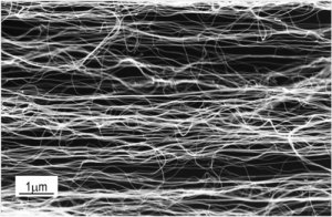
EM image of multi-walled carbon nanotube sheet used for thermo-electromagnetic sound transducer. (Image: Mikhail Kozlov, University of Texas at Dallas)

EM image of multi-walled carbon nanotube sheet used for thermo-electromagnetic sound transducer. (Image: Mikhail Kozlov, University of Texas at Dallas)

Kozlov goes on to explain his work in more detail,

… a hybrid thermo-electromagnetic sound transducer (TEMST) [was] fabricated using highly porous multi-walled carbon nanotube sheet that was placed in the proximity of a permanent magnet. Upon electrical AC excitation, thermal response of the material is combined with diaphragm-like sheet oscillations induced by the electromagnetic action of the Lorentz force.

Unlike conventional diaphragm loudspeaker, acoustic spectrum of the TEMST device consists of a superposition of TA and EM responses that can be altered by applied bias voltage. Variation of bias voltage changes spectral intensity and spatial distribution of generated sound.

In particular, propagation direction of the sound can be reversed by switching bias polarity that somewhat resembles voltage-controlled acoustic reflection. Such uncommon behavior was explained by interference of the two contributions being beneficial for diverse sound management applications.

It was found also that amplitude of first TEMST harmonic changes a lot with applied magnetic field, while the second one remains almost field independent. This unusual feature is convenient for magnetic sensing similar to that enabled by Lorentz force magnetometers. The magnetic field detection in the TEMST device is facilitated by the audio sensing system.

Here’s a link to and a citation for the paper,

Thermo-electromagnetic sound transducer based on carbon nanotube sheet by Mikhail Kozlov and Jiyoung Oh. J. Appl. Phys. 116, 094301 (2014); http://dx.doi.org/10.1063/1.4894143 Published online Sept. 2, 2014

This paper is behind a paywall.

It takes more than research to change energy sources and use

Much of the talk about reducing or eliminating dependency on fossil fuels is focused on research to accomplish these goals or policies to support and promote new patterns of energy use as opposed to the details needed to implement a change in the infrastructures. For example, one frequently sees news about various energy research efforts such as this one at the University of Texas at Dallas featured in a Feb. 14, 2013 news item on Azonano,

University of Texas at Dallas researchers and their colleagues at other institutions are investigating ways to harvest energy from such diverse sources as mechanical vibrations, wasted heat, radio waves, light and even movements of the human body.

The goal is to develop ways to convert this unused energy into a form that can self-power the next generation of electronics, eliminating or reducing the need for bulky, limited-life batteries.

Beyond the more familiar wind and solar power, energy harvesting has a wide range of potential applications. These include: powering wireless sensor networks placed in “intelligent” buildings, or in hard-to-reach or dangerous areas; monitoring the structural health of aircraft; and biomedical implants that might transmit health data to your doctor or treat a chronic condition.

The Feb. 14, 2013 University of Texas at Dallas news release, which originated the news item, describes a recent energy research event and highlights some of the work being performed by the Center for Energy Harvesting Materials and Systems (CEHMS) consortium (Note: A link has been removed),

At a recent scientific conference held at UT Dallas, experts from academia, industry and government labs gathered to share their latest research on energy harvesting. Energy Summit 2013 focused on research initiatives at UT Dallas, Virginia Tech and Leibniz University in Germany, which form a consortium called the Center for Energy Harvesting Materials and Systems (CEHMS).

Founded in 2010, CEHMS is an Industry/University Cooperative Research Center funded in part by the National Science Foundation. It includes not only academic institutions, but also corporate members who collaborate on research projects and also provide funding for the center.  Roger Nessen, manager of sales and marketing at Exelis Inc. is chairman of the CEHMS advisory board.

Here are some examples of the research,

For example, Dr. Mario Rotea, the Erik Jonsson Chair and head of the Department of Mechanical Engineering at UT Dallas, discussed some of his work aimed at advancing the development of wind energy systems. He represents UT Dallas in a proposed new consortium of universities and companies called WindSTAR that would collaborate with CEHMS on wind energy science and technology issues.

On the chemistry front, Smith’s [Dennis Smith, co-director of CEHMS and the Robert A. Welch Distinguished Chair in Chemistry at UT Dallas] synthetic chemistry lab is working with advanced materials that use piezoelectrics. If a piezoelectric material is deformed by a mechanical stress – such as stepping on it or subjecting it to vibrations – it produces an electric current. Smith’s lab is investigating whether the addition of nanoparticles to certain piezoelectric materials can boost this so-called piezoelectric effect.

CEHMS co-director Dr. Shashank Priya, professor of mechanical engineering and the James and Elizabeth Turner Fellow of Engineering at Virginia Tech, collaborates with Smith on piezoelectric research. Among many projects, researchers at Virginia Tech are incorporating piezoelectrics into “smart” tiles that produce electricity when stepped upon, as well as into materials that might be applied like wallpaper to gather light and vibrational energy from walls.

Other university and industry projects include:

  • Investigating how to redesign systems to require less power.
  • An intelligent tire system that harvests energy from the vibrations in a rotating tire, powering embedded sensors that gather and report data on tire pressure, tire conditions and road conditions.
  • A new class of magnetoelectric materials that can simultaneously convert magnetic fields and vibrations into energy.
  • A textile-type material that converts wasted thermal energy into electricity, which could be wrapped around hot pipes or auto exhaust pipes to generate power.
  • Flexible solar cells that could be integrated into textiles, and worn by hikers or soldiers to power portable electronic devices far away from an electric socket.

It’s exciting to talk about research, startups, and policies but at some point one needs to develop an infrastructure to support these efforts as Kyle Vanhemert points out (in an elliptical fashion) in his Feb.14, 2013 article, A Deeply Thought-Out Plan for EV [electric vehicle] Charging Stations, on the Fast Company website,

Currently, the best estimates suggest that upwards of 80% of electric vehicle charging happens at home. … If we want to see wider adoption of EVs, however, one thing is obvious: We need to make it possible for drivers to charge in places other than their garage. It’s a more complex problem than it might seem, but a series of reports by the New York-based architecture and design studio WXY will at least give urban planners and prospective charging station entrepreneurs a place to start.

The studies, sponsored by the U.S. Department of Energy and the New York State Energy Research and Development Authority, address a major obstacle standing in the way of more ubiquitous charging–namely, that no one knows exactly what ubiquitous charging looks like. And in fairness, that’s because it doesn’t look like any one thing.  …

The WXY design studio has developed guidelines for these hypothetical EV charging stations,

The study identifies 22 design elements in all, divided into three categories: installation, access, and operation. The first looks at the infrastructural nuts and bolts of the site, including factors like physical dimensions of the station and its proximity to the power grid. Access deals with the factors that shape the basic user experience, things like proximity to traffic and building entrances, lighting, and signage. …

Vanhemert’s article includes some design diagrams, more details about these charging stations, and links to the design studio’s report and other reports that have been commissioned for the US Northeast Electric Vehicle Network.

Thank you to Kyle Vanhemert for a thought-provoking article, which raises questions about what kinds of changes will need to be made to infrastructure and everyday gadgets as we transition to new energy sources.

Robotic sea jellies (jellyfish) and carbon nanotubes

After my recent experience at the Vancouver Aquarium (Jan.19.12 posting) where I was informed that jellyfish are now called sea jellies, I was not expecting to see the term jellyfish still in use. I gather the new name is not being used universally yet, which explains the title for a March 23, 2012 news item on Nanowerk, Robotic jellyfish built on nanotechnology,

Researchers at The University of Texas at Dallas and Virginia Tech have created an undersea vehicle inspired by the common jellyfish that runs on renewable energy and could be used in ocean rescue and surveillance missions.

In a study published this week in Smart Materials and Structures (“Hydrogen-fuel-powered bell segments of biomimetic jellyfish”), scientists created a robotic jellyfish, dubbed Robojelly, that feeds off hydrogen and oxygen gases found in water.

“We’ve created an underwater robot that doesn’t need batteries or electricity,” said Dr. Yonas Tadesse, assistant professor of mechanical engineering at UT Dallas and lead author of the study. “The only waste released as it travels is more water.”

Engineers and scientists have increasingly turned to nature for inspiration when creating new technologies. The simple yet powerful movement of the moon jellyfish made it an appealing animal to simulate.

The March 22, 2012 press release from the University of Texas at Dallas features images and a video in addition to its text. From the press release,

The Robojelly consists of two bell-like structures made of silicone that fold like an umbrella. Connecting the umbrella are muscles that contract to move.

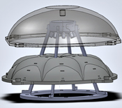
Here’s a computer-aided image,

A computer-aided model of Robojelly shows the vehicle's two bell-like structures.

Here’s what the robojelly looks like,

The Robojelly, shown here out of water, has an outer structure made out of silicone.

This robojelly differs from the original model,which was battery-powered. Here’s a video of the original robojelly,

The new robojelly has artificial muscles(from the Mar. 22, 2012 University of Texas at Dallas press release),

In this study, researchers upgraded the original, battery-powered Robojelly to be self-powered. They did that through a combination of high-tech materials, including artificial muscles that contract when heated.

These muscles are made of a nickel-titanium alloy wrapped in carbon nanotubes, coated with platinum and housed in a pipe. As the mixture of hydrogen and oxygen encounters the platinum, heat and water vapor are created. That heat causes a contraction that moves the muscles of the device, pumping out the water and starting the cycle again.

“It could stay underwater and refuel itself while it is performing surveillance,” Tadesse said.

In addition to military surveillance, Tadesse said, the device could be used to detect pollutants in water.

This is a study that has been funded by the US Office of Naval Research. At the next stage, researchers want to make the robojelly’s legs work independently so it can travel in more than one direction.

Asia’s research effort in nano-, bio-, and information technology integrated in Asian Research Network

The Feb. 29, 2012 news item by Cameron Chai on Azonano spells it out,

An Asian Research Network (ARN) has been formed by the Hanyang University of Korea and RIKEN of Japan in collaboration with other institutes and universities in Asia. This network has been launched to reinforce a strong education and research collaboration throughout Asia.

The Asian Research Network website is here. You will need to use your scroll bars as it appears to be partially constructed (or maybe my system is so creaky that I just can’t see everything on the page). Towards the bottom (right side) of the home page,there are a couple of red buttons for PDFs of the ARN Pamphlet and Research Articles.

From page 2 of the ARN pamphlet, here’s a listing of the member organizations,

KOREA

Hanyang University
Samsung Electronics
Electronics and Telecommunication Research Institute
Seoul National University
Institute of Pasteur Korea
Korea Research Institute of Chemical Technology
Korea Advanced Nano Fab Center

JAPAN

RIKEN

INDIA

National Chemical Laboratory
Shivaji University
Indian Institutes of Science Education and Research
Pune University
Indian Institute of Technology-Madras (In Progress)
Indian Institute of Science (In Progress)

USA

University of Texas at Dallas
UCLA (In Progress)
f d i i ( )

CHINA

National Center for Nanoscience and Technology
Peking University

SINGAPORE

National University of Singapore
Nanyang Technological University (In Progress)
Stanford University In Progress)
University of Maryland (In Progress)

ISRAEL

Weizmann Institute of Science (In Progress)
Hebrew University Jerusalem

THAILAND

National Science and Technology Development Agency (In Progress)

I was a little surprised to see Israel on the list and on an even more insular note, why no Canada?

Getting back to the ARN, here are their aims, from page 2 of the ARN pamphlet,

We are committed to fostering talented human resources, creating a research network in which researchers in the region share their knowledge and experiences, and establishing a future-oriented partnership to globalize our research capabilities. To this end, we will achieve excellence in all aspects of education, research, and development in the area of fusion research between BT [biotechnology] and IT [information technology] based on NT [nanotechnology] in general. We will make a substantial contribution to the betterment of the global community as well as the Asian society.

I look forward to hearing more from them in the future.