Tag Archives: University of Warsaw

Fluid mechanics in the kitchen

Caption: Dr. Maciej Lisicki is developing a formula for perfectly creamy ice cream in his laboratory. Credit Photo: Michal Czerepaniak, source: Faculty of Physics, University of Warsaw.

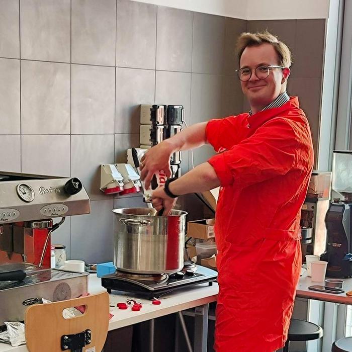
It’s unusual to see a scientist in an orange (maybe it could be called fire engine red?) jumpsuit as it has an altogether different meaning (prison wear) in the US.

Sadly, there isn’t a video of Dr. Maciej Lisicki or other scientists in the kitchen but here’s a description of what they’ve been up to from a June 22, 2023 University of Warsaw (Poland) press release (also on EurekAlert),

Take four brilliant physicists who specialize in fluid mechanics and put them in the kitchen. Give them pots, pans, basic foodstuffs, and a bottle of champagne. Add a COVID-19 pandemic, a pinch of boredom, and a handful of good ideas. Stir, wait, and voilà – you have a “delicious” publication that will teach you how bubbles are created in champagne, how to brew the perfect espresso, and how “kitchen revolutions” can contribute to innovations in many fields, including biomedicine and nanotechnology.

Most of us visit this place every day. But the kitchen is not just for cooking meals. “It can be an excellent place to conduct experiments and even make scientific discoveries,” argues Maciej Lisicki, of the Faculty of Physics of the University of Warsaw, co-author of a publication in the prestigious journal Reviews of Modern Physics. The team of researchers, which in addition to Maciej Lisicki includes Arnold Mathijssen of the University of Pennsylvania, Endre J.L. Mossige of the University of Oslo and Vivek N. Prakash of the University of Miami, not only explores the history of food science, but also shows how phenomena in the kitchen lead to innovations in biomedicine and nanotechnology.

COVID pandemic and bubbles in champagne

Maciej Lisicki and his fellow researchers began working on the article during the COVID-19 pandemic, when many researchers could not work in the lab and began experimenting in their homes. “It started primarily with the intention to make an educational tool, given that kitchens offer a low barrier of entry to doing science — all you need are some pots, pans, and a few ingredients to get a few reactions going—but it quickly grew into a more scientific reflection of the history of food once we realized how interwoven the fields are,” says Arnold Mathijssen.

The team of researchers constructed the results of their work along the lines of a menu. “Tasting” begins with the physics of drinks and cocktails, then moves on to main courses, and finishes with coffee and desserts, whose preparation is also based on the intuitive use of the laws of nature.

As with any good party, everything begins with the opening of a bottle of champagne. After a characteristic “pop”, we observe how a mist forms around the neck of the bottle. – This phenomenon is associated with a rapid change in pressure. Inside the bottle it reaches almost five atmospheres, but when the bottle is opened it drops to one atmosphere.  “The expansion is accompanied by a drop in temperature, which causes the water vapor that accumulates near the mouth of the bottle to freeze, and the carbon dioxide coming out of the bottle to condense”, Maciej Lisicki explains.

In their paper, the researchers also look at bubbles, which give sparkling wines their unique flavor. “Circulating bubbles force the transport of the liquid in the glass, and thus facilitate the release and spread of aromatic notes and flavors”, the researcher adds. From the section of the paper devoted to drinks and cocktails, we will also learn what makes the foam in beer so thick and stable, why aniseed drinks such as rakija and ouzo get cloudy when enough water is added (the phenomenon is even called the “ouzo effect”), and what “tears of wine” are.

When water surfs the pan

Moving on to the main course, the scientists explain the role of heat and its effect on food textures, aromas, and flavors. Among other things, they describe the Leidenfrost effect, in which a drop of liquid placed on a very hot surface forms an insulating layer of vapor, that prevents rapid boiling. “Water drops thrown onto the pan ‘surf’ and even bounce off the surface, instead of evaporating immediately”, Lisicki says. 

Proper temperature is crucial in the preparation of many foods. “It doesn’t take a Ph.D. in physics to fry the perfect steak. Everyone knows that one needs to quickly sear the meat in a sufficiently hot pan. As a result, the proteins on the surface of the steak coagulate and the moisture is kept inside”, the researcher explains. 

A Ph.D. in dishwashing

The text also includes examples of scientific discoveries that researchers have made without leaving their own kitchens. One of them is related to the biography of Agnes Pockels.

“Her story speaks of the inequality in science. She was a woman in Germany in the late 19th century, so she was not allowed to attend university for formal training, making it difficult for her to submit her research to journals,” Mathijssen says.

Running her parents’ household and spending a lot of time in the kitchen, she quickly began experimenting there. “Observing the formation of foam and films on the surface of dirty dishes, she was the first to describe the phenomenon of surface tension and developed an instrument to measure it. Initially, scientific journals were reluctant to publish the results of her experiments due to her lack of formal training and affiliation with university staff. Her first paper was published through Lord Rayleigh in Nature and contributed to the understanding of surface effects in liquids. Agnes Pockels then became well-known and respected, and all her subsequent work was published in high-profile journals. This example shows that it is possible to become a respected scientist without leaving home,” notes Maciej Lisicki.

Salad dressing vs. nanoengineering

Research in fluid mechanics can help improve food processing technologies, as well as find applications in other fields such as nanoengineering and medicine. “In an earlier study (“Rechargeable self-assembled droplet microswimmers driven by surface phase transitions”, published in Nature Physics) conducted by my team, we used a simple emulsion that is the basis of salad dressings – oil with water. We were able to make droplets of such an emulsion, with the addition of a surfactant, form tendrils under temperature and move like bacteria. Such nontoxic, biocompatible microfluidics could be used in the future, for example, to precisely deliver drugs anywhere in our bodies”, Lisicki explains. 

The review also highlights the applicability of these technologies in areas such as food safety and quality control. By deploying devices that can detect food-borne pathogens or toxins using principles of fluid dynamics, the scientific community can contribute significantly to public health.

Another key aspect of their review is the potential impact it could have on policy decisions, particularly those related to environmental sustainability and food safety. The authors highlight the significance of science-based policies, for example – referencing the announced EU ban on PFAS non-stick coatings by 2030. Using the scientific understanding offered by studies like these, policy makers can make informed decisions to foster a more sustainable and safer food future.

“Kitchen flows show us that significant scientific problems are available at our fingertips and do not always require space technology to explore them. On the other hand, more than a few cosmic technologies were born from inspiration by everyday phenomena. The kitchen can therefore entertain us, but also teach us – in this case, physics. This is why it is worth a try to unleash your curiosity and experiment!” Lisicki adds.

This research was supported by the United States Department of Agriculture (USDA-NIFA AFRI 2020-67017-30776 and 2020-67015-32330).

Faculty of Physics of the University of Warsaw
Physics and astronomy at the University of Warsaw appeared in 1816 as part of the then Faculty of Philosophy. In 1825, the Astronomical Observatory was established. Currently, the Faculty of Physics at the University of Warsaw consists of the following institutes: Experimental Physics, Theoretical Physics, Geophysics, the Department of Mathematical Methods and the Astronomical Observatory. The research covers almost all areas of modern physics, on scales from quantum to cosmological. The Faculty’s research and teaching staff consists of over 200 academic teachers, 88 of whom are professors. About 1,100 students and over 170 doctoral students study at the Faculty of Physics at the University of Warsaw.

Perhaps the paper provides more information about the ice cream research depicted in the visual image at the top of this posting. Here’s a link to and a citation for the paper,

Culinary fluid mechanics and other currents in food science by Arnold J. T. M. Mathijssen, Maciej Lisicki, Vivek N. Prakash, and Endre J. L. Mossige. Rev. Mod. Phys. Vol. 95, Iss. 2 — April – June 2023 025004 DOI: https://doi.org/10.1103/RevModPhys.95.025004 Published: 5 June 2023 © 2023 American Physical Society

This paper is behind a paywall.

Entangling a single photon with a trillion atoms

Polish scientists have cast light on an eighty-year old ‘paradox’ according to a March 2, 2017 news item on plys.org,

A group of researchers from the Faculty of Physics at the University of Warsaw has shed new light on the famous paradox of Einstein, Podolsky and Rosen after 80 years. They created a multidimensional entangled state of a single photon and a trillion hot rubidium atoms, and stored this hybrid entanglement in the laboratory for several microseconds. …

In their famous Physical Review article, published in 1935, Einstein, Podolsky and Rosen considered the decay of a particle into two products. In their thought experiment, two products of decay were projected in exactly opposite directions—or more scientifically speaking, their momenta were anti-correlated. Though not be a mystery within the framework of classical physics, when applying the rules of quantum theory, the three researchers arrived at a paradox. The Heisenberg uncertainty principle, dictating that position and momentum of a particle cannot be measured at the same time, lies at the center of this paradox. In Einstein’s thought experiment, it is possible to measure the momentum of one particle and immediately know the momentum of the other without measurement, as it is exactly opposite. Then, by measuring the position of the second particle, the Heisenberg uncertainty principle is seemingly violated, an apparent paradox that seriously baffled the three physicists.

A March 2, 2017 University of Warsaw press release (also on EurekAlert), which originated the news item, expands on the topic,

Only today we know that this experiment is not, in fact, a paradox. The mistake of Einstein and co-workers was to use one-particle uncertainty principle to a system of two particles. If we treat these two particles as described by a single quantum state, we learn that the original uncertainty principle ceases to apply, especially if these particles are entangled.

In the Quantum Memories Laboratory at the University of Warsaw, the group of three physicists was first to create such an entangled state consisting of a macroscopic object – a group of about one trillion atoms, and a single photon – a particle of light. “Single photons, scattered during the interaction of a laser beam with atoms, are registered on a sensitive camera. A single registered photon carries information about the quantum state of the entire group of atoms. The atoms may be stored, and their state may be retrieved on demand.” – says Michal Dabrowski, PhD student and co-author of the article.

The results of the experiment confirm that the atoms and the single photon are in a joint, entangled state. By measuring position and momentum of the photon, we gain all information about the state of atoms. To confirm this, polish scientists convert the atomic state into another photon, which again is measured using the state-of-the-art camera developed in the Quantum Memories Laboratory. “We demonstrate the Einstein-Podolsky-Rosen apparent paradox in a very similar version as originally proposed in 1935, however we extend the experiment by adding storage of light within the large group of atoms. Atoms store the photon in a form of a wave made of atomic spins, containing one trillion atoms. Such a state is very robust against loss of a single atoms, as information is spread across so many particles.” – says Michal Parniak, PhD student taking part in the study.

The experiment performed by the group from the University of Warsaw is unique in one other way as well. The quantum memory storing the entangled state, created thanks to “PRELUDIUM” grant from the Poland’s National Science Centre and “Diamentowy Grant” from the Polish Ministry of Science and Higher Education, allows for storage of up to 12 photons at once. This enhanced capacity is promising in terms of applications in quantum information processing. “The multidimensional entanglement is stored in our device for several microseconds, which is roughly a thousand times longer than in any previous experiments, and at the same time long enough to perform subtle quantum operations on the atomic state during storage” – explains Dr. Wojciech Wasilewski, group leader of the Quantum Memories Laboratory team.

The entanglement in the real and momentum space, described in the Optica article, can be used jointly with other well-known degrees of freedom such as polarization, allowing generation of so-called hyper-entanglement. Such elaborate ideas constitute new and original test of the fundamentals of quantum mechanics – a theory that is unceasingly mysterious yet brings immense technological progress.

Here’s a link to and a citation for the paper,

Einstein–Podolsky–Rosen paradox in a hybrid bipartite system by Michał Dąbrowski, Michał Parniak, and Wojciech Wasilewski. Optica Vol. 4, Issue 2, pp. 272-275 (2017) •https://doi.org/10.1364/OPTICA.4.000272

This paper appears to be open access.

First hologram of a single photon (light particle)

Polish scientists have created a technique for something thought to be impossible. From a July 19, 2016 news item on Nanowerk,

Until quite recently, creating a hologram of a single photon was believed to be impossible due to fundamental laws of physics. However, scientists at the Faculty of Physics, University of Warsaw, have successfully applied concepts of classical holography to the world of quantum phenomena. A new measurement technique has enabled them to register the first ever hologram of a single light particle, thereby shedding new light on the foundations of quantum mechanics.

A July 18, 2016 University of Warsaw press release on EurekAlert, which originated the news item, describes the breakthrough in more detail,

Scientists at the Faculty of Physics, University of Warsaw, have created the first ever hologram of a single light particle. The spectacular experiment, reported in the prestigious journal Nature Photonics, was conducted by Dr. Radoslaw Chrapkiewicz and Michal Jachura under the supervision of Dr. Wojciech Wasilewski and Prof. Konrad Banaszek. Their successful registering of the hologram of a single photon heralds a new era in holography: quantum holography, which promises to offer a whole new perspective on quantum phenomena.

“We performed a relatively simple experiment to measure and view something incredibly difficult to observe: the shape of wavefronts of a single photon,” says Dr. Chrapkiewicz.

In standard photography, individual points of an image register light intensity only. In classical holography, the interference phenomenon also registers the phase of the light waves (it is the phase which carries information about the depth of the image). When a hologram is created, a well-described, undisturbed light wave (reference wave) is superimposed with another wave of the same wavelength but reflected from a three-dimensional object (the peaks and troughs of the two waves are shifted to varying degrees at different points of the image). This results in interference and the phase differences between the two waves create a complex pattern of lines. Such a hologram is then illuminated with a beam of reference light to recreate the spatial structure of wavefronts of the light reflected from the object, and as such its 3D shape.

One might think that a similar mechanism would be observed when the number of photons creating the two waves were reduced to a minimum, that is to a single reference photon and a single photon reflected by the object. And yet you’d be wrong! The phase of individual photons continues to fluctuate, which makes classical interference with other photons impossible. Since the Warsaw physicists were facing a seemingly impossible task, they attempted to tackle the issue differently: rather than using classical interference of electromagnetic waves, they tried to register quantum interference in which the wave functions of photons interact.

Wave function is a fundamental concept in quantum mechanics and the core of its most important equation: the Schrödinger equation. In the hands of a skilled physicist, the function could be compared to putty in the hands of a sculptor: when expertly shaped, it can be used to ‘mould’ a model of a quantum particle system. Physicists are always trying to learn about the wave function of a particle in a given system, since the square of its modulus represents the distribution of the probability of finding the particle in a particular state, which is highly useful.

“All this may sound rather complicated, but in practice our experiment is simple at its core: instead of looking at changing light intensity, we look at the changing probability of registering pairs of photons after the quantum interference,” explains doctoral student Jachura.

Why pairs of photons? A year ago, Chrapkiewicz and Jachura used an innovative camera built at the University of Warsaw to film the behaviour of pairs of distinguishable and non-distinguishable photons entering a beam splitter. When the photons are distinguishable, their behaviour at the beam splitter is random: one or both photons can be transmitted or reflected. Non-distinguishable photons exhibit quantum interference, which alters their behaviour: they join into pairs and are always transmitted or reflected together. This is known as two-photon interference or the Hong-Ou-Mandel effect.

“Following this experiment, we were inspired to ask whether two-photon quantum interference could be used similarly to classical interference in holography in order to use known-state photons to gain further information about unknown-state photons. Our analysis led us to a surprising conclusion: it turned out that when two photons exhibit quantum interference, the course of this interference depends on the shape of their wavefronts,” says Dr. Chrapkiewicz.

Quantum interference can be observed by registering pairs of photons. The experiment needs to be repeated several times, always with two photons with identical properties. To meet these conditions, each experiment started with a pair of photons with flat wavefronts and perpendicular polarisations; this means that the electrical field of each photon vibrated in a single plane only, and these planes were perpendicular for the two photons. The different polarisation made it possible to separate the photons in a crystal and make one of them ‘unknown’ by curving their wavefronts using a cylindrical lens. Once the photons were reflected by mirrors, they were directed towards the beam splitter (a calcite crystal). The splitter didn’t change the direction of vertically-polarised photons, but it did diverge diplace horizontally-polarised photons. In order to make each direction equally probable and to make sure the crystal acted as a beam splitter, the planes of photon polarisation were bent by 45 degrees before the photons entered the splitter. The photons were registered using the state-of-the-art camera designed for the previous experiments. By repeating the measurements several times, the researchers obtained an interference image corresponding to the hologram of the unknown photon viewed from a single point in space. The image was used to fully reconstruct the amplitude and phase of the wave function of the unknown photon.

The experiment conducted by the Warsaw physicists is a major step towards improving our understanding of the fundamental principles of quantum mechanics. Until now, there has not been a simple experimental method of gaining information about the phase of a photon’s wave function. Although quantum mechanics has many applications, and it has been verified many times with a great degree of accuracy over the last century, we are still unable to explain what wave functions actually are: are they simply a handy mathematical tool, or are they something real?

“Our experiment is one of the first allowing us to directly observe one of the fundamental parameters of photon’s wave function – its phase – bringing us a step closer to understanding what the wave function really is,” explains Jachura.

The Warsaw physicists used quantum holography to reconstruct wave function of an individual photon. Researchers hope that in the future they will be able to use a similar method to recreate wave functions of more complex quantum objects, such as certain atoms. Will quantum holography find applications beyond the lab to a similar extent as classical holography, which is routinely used in security (holograms are difficult to counterfeit), entertainment, transport (in scanners measuring the dimensions of cargo), microscopic imaging and optical data storing and processing technologies?

“It’s difficult to answer this question today. All of us – I mean physicists – must first get our heads around this new tool. It’s likely that real applications of quantum holography won’t appear for a few decades yet, but if there’s one thing we can be sure of it’s that they will be surprising,” summarises Prof. Banaszek.

Here’s a link to and a citation for the paper,

Hologram of a single photon by Radosław Chrapkiewicz, Michał Jachura, Konrad Banaszek, & Wojciech Wasilewski.  Nature Photonics (2016) doi:10.1038/nphoton.2016.129 Published online 18 July 2016

This paper is behind a paywall.

Transition metal dichalcogenides (molybdenum disulfide and tungsten diselenide) rock the graphene boat

Anyone who’s read stories about scientific discovery knows that the early stages are characterized by a number of possibilities so the current race to unseat graphene as the wonder material of the nanoworld is a ‘business as usual’ sign although I imagine it can be confusing for investors and others hoping to make their fortunes. As for the contenders to the ‘wonder nanomaterial throne’, they are transition metal dichalcogenides: molybdenum disulfide and tungsten diselenide both of which have garnered some recent attention.

A March 12, 2014 news item on Nanwerk features research on molybdenum disulfide from Poland,

Will one-atom-thick layers of molybdenum disulfide, a compound that occurs naturally in rocks, prove to be better than graphene for electronic applications? There are many signs that might prove to be the case. But physicists from the Faculty of Physics at the University of Warsaw have shown that the nature of the phenomena occurring in layered materials are still ill-understood and require further research.

….

Researchers at the University of Warsaw, Faculty of Physics (FUW) have shown that the phenomena occurring in the crystal network of molybdenum disulfide sheets are of a slightly different nature than previously thought. A report describing the discovery, achieved in collaboration with Laboratoire National des Champs Magnétiques Intenses in Grenoble, has recently been published in Applied Physics Letters.

“It will not become possible to construct complex electronic systems consisting of individual atomic sheets until we have a sufficiently good understanding of the physics involved in the phenomena occurring within the crystal network of those materials. Our research shows, however, that research still has a long way to go in this field”, says Prof. Adam Babinski at the UW Faculty of Physics.

A March 12, 2014 Dept. of Physics University of Warsaw (FUW) news release, which originated the news item, describes the researchers’ ideas about graphene and alternative materials such as molybdenum disulfide,

“It will not become possible to construct complex electronic systems consisting of individual atomic sheets until we have a sufficiently good understanding of the physics involved in the phenomena occurring within the crystal network of those materials. Our research shows, however, that research still has a long way to go in this field”, says Prof. Adam Babiński at the UW Faculty of Physics.

The simplest method of creating graphene is called exfoliation: a piece of scotch tape is first stuck to a piece of graphite, then peeled off. Among the particles that remain stuck to the tape, one can find microscopic layers of graphene. This is because graphite consists of many graphene sheets adjacent to one another. The carbon atoms within each layer are very strongly bound to one another (by covalent bonds, to which graphene owes its legendary resilience), but the individual layers are held together by significantly weaker bonds (van de Walls [van der Waals] bonds). Ordinary scotch tape is strong enough to break the latter and to tear individual graphene sheets away from the graphite crystal.

A few years ago it was noticed that just as graphene can be obtained from graphite, sheets a single atom thick can similarly be obtained from many other crystals. This has been successfully done, for instance, with transition metals chalcogenides (sulfides, selenides, and tellurides). Layers of molybdenum disulfide (MoS2), in particular, have proven to be a very interesting material. This compound exists in nature as molybdenite, a crystal material found in rocks around the world, frequently taking the characteristic form of silver-colored hexagonal plates. For years molybdenite has been used in the manufacturing of lubricants and metal alloys. Like in the case of graphite, the properties of single-atom sheets of MoS2 long went unnoticed.

From the standpoint of applications in electronics, molybdenum disulfide sheets exhibit a significant advantage over graphene: they have an energy gap, an energy range within which no electron states can exist. By applying electric field, the material can be switched between a state that conducts electricity and one that behaves like an insulator. By current calculations, a switched-off molybdenum disulfide transistor would consume even as little as several hundred thousand times less energy than a silicon transistor. Graphene, on the other hand, has no energy gap and transistors made of graphene cannot be fully switched off.

The news release goes on to describe how the researchers refined their understanding of molybdenum disulfide and its properties,

Valuable information about a crystal’s structure and phenomena occurring within it can be obtained by analyzing how light gets scattered within the material. Photons of a given energy are usually absorbed by the atoms and molecules of the material, then reemitted at the same energy. In the spectrum of the scattered light one can then see a distinctive peak, corresponding to that energy. It turns out, however, that one out of many millions of photons is able to use some of its energy otherwise, for instance to alter the vibration or circulation of a molecule. The reverse situation also sometimes occurs: a photon may take away some of the energy of a molecule, and so its own energy slightly increases. In this situation, known as Raman scattering, two smaller peaks are observed to either side of the main peak.

The scientists at the UW Faculty of Physics analyzed the Raman spectra of molybdenum disulfide carrying on low-temperature microscopic measurements. The higher sensitivity of the equipment and detailed analysis methods enabled the team to propose a more precise model of the phenomena occurring in the crystal network of molybdenum disulfide.

“In the case of single-layer materials, the shape of the Raman lines has previously been explained in terms of phenomena involving certain characteristic vibrations of the crystal network. We have shown for molybdenum disulfide sheets that the effects ascribed to those vibrations must actually, at least in part, be due to other network vibrations not previously taken into account”, explains Katarzyna Gołasa, a doctorate student at the UW Faculty of Physics.

The presence of the new type of vibration in single-sheet materials has an impact on how electrons behave. As a consequence, these materials must have somewhat different electronic properties than previously anticipated.

Here’s what the rocks look like,

Molybdenum disulfide occurs in nature as molybdenite, crystalline material that frequently takes the characteristic form of silver-colored hexagonal plates. (Source: FUW)

Molybdenum disulfide occurs in nature as molybdenite, crystalline material that frequently takes the characteristic form of silver-colored hexagonal plates. (Source: FUW)

I am not able to find the published research at this time (March 13, 2014).

The tungsten diselenide story is specifically application-centric. Dexter Johnson in a March 11, 2014 post on his Nanoclast blog (on the IEEE [Institute of Electrical and Electronics Engineers] website) describes the differing perspectives and potential applications suggested by the three teams that cooperated to produce papers united by a joint theme ,

The three research groups focused on optoelectronics applications of tungsten diselenide, but each with a slightly different emphasis.

The University of Washington scientists highlighted applications of the material for a light emitting diode (LED). The Vienna University of Technology group focused on the material’s photovoltaic applications. And, finally, the MIT [Massachusetts Institute of Technology] group looked at all of the optoelectronic applications for the material that would result from the way it can be switched from being a p-type to a n-type semiconductor.

Here are some details of the research from each of the institutions’ news releases.

A March 10, 2014 University of Washington (state) news release highlights their LED work,

University of Washington [UW] scientists have built the thinnest-known LED that can be used as a source of light energy in electronics. The LED is based off of two-dimensional, flexible semiconductors, making it possible to stack or use in much smaller and more diverse applications than current technology allows.

“We are able to make the thinnest-possible LEDs, only three atoms thick yet mechanically strong. Such thin and foldable LEDs are critical for future portable and integrated electronic devices,” said Xiaodong Xu, a UW assistant professor in materials science and engineering and in physics.

The UW’s LED is made from flat sheets of the molecular semiconductor known as tungsten diselenide, a member of a group of two-dimensional materials that have been recently identified as the thinnest-known semiconductors. Researchers use regular adhesive tape to extract a single sheet of this material from thick, layered pieces in a method inspired by the 2010 Nobel Prize in Physics awarded to the University of Manchester for isolating one-atom-thick flakes of carbon, called graphene, from a piece of graphite.

In addition to light-emitting applications, this technology could open doors for using light as interconnects to run nano-scale computer chips instead of standard devices that operate off the movement of electrons, or electricity. The latter process creates a lot of heat and wastes power, whereas sending light through a chip to achieve the same purpose would be highly efficient.

“A promising solution is to replace the electrical interconnect with optical ones, which will maintain the high bandwidth but consume less energy,” Xu said. “Our work makes it possible to make highly integrated and energy-efficient devices in areas such as lighting, optical communication and nano lasers.”

Here’s a link to and a citation for this team’s paper,

Electrically tunable excitonic light-emitting diodes based on monolayer WSe2 p–n junctions by Jason S. Ross, Philip Klement, Aaron M. Jones, Nirmal J. Ghimire, Jiaqiang Yan, D. G. Mandrus, Takashi Taniguchi, Kenji Watanabe, Kenji Kitamura, Wang Yao, David H. Cobden, & Xiaodong Xu. Nature Nanotechnology (2014) doi:10.1038/nnano.2014.26 Published online 09 March 2014

This paper is behind a paywall.

A March 9, 2014 University of Vienna news release highlights their work on tungsten diselinide and its possible application in solar cells,

… With graphene as a light detector, optical signals can be transformed into electric pulses on extremely short timescales.

For one very similar application, however, graphene is not well suited for building solar cells. “The electronic states in graphene are not very practical for creating photovoltaics”, says Thomas Mueller. Therefore, he and his team started to look for other materials, which, similarly to graphene, can arranged in ultrathin layers, but have even better electronic properties.

The material of choice was tungsten diselenide: It consists of one layer of tungsten atoms, which are connected by selenium atoms above and below the tungsten plane. The material absorbs light, much like graphene, but in tungsten diselenide, this light can be used to create electrical power.

The layer is so thin that 95% of the light just passes through – but a tenth of the remaining five percent, which are absorbed by the material, are converted into electrical power. Therefore, the internal efficiency is quite high. A larger portion of the incident light can be used if several of the ultrathin layers are stacked on top of each other – but sometimes the high transparency can be a useful side effect. “We are envisioning solar cell layers on glass facades, which let part of the light into the building while at the same time creating electricity”, says Thomas Mueller.

Today, standard solar cells are mostly made of silicon, they are rather bulky and inflexible. Organic materials are also used for opto-electronic applications, but they age rather quickly. “A big advantage of two-dimensional structures of single atomic layers is their crystallinity. Crystal structures lend stability”, says Thomas Mueller.

Here’s a link to and a citation for the University of Vienna paper,

Solar-energy conversion and light emission in an atomic monolayer p–n diode by Andreas Pospischil, Marco M. Furchi, & Thomas Mueller. Nature Nanotechnology (2014) doi:10.1038/nnano.2014.14 Published online 09 March 2014

This paper is behind a paywll.

Finally, a March 10, 2014 MIT news release details their work about material able to switch from p-type (p = positive) to a n-type (n = negative) semiconductors,

The material they used, called tungsten diselenide (WSe2), is part of a class of single-molecule-thick materials under investigation for possible use in new optoelectronic devices — ones that can manipulate the interactions of light and electricity. In these experiments, the MIT researchers were able to use the material to produce diodes, the basic building block of modern electronics.

Typically, diodes (which allow electrons to flow in only one direction) are made by “doping,” which is a process of injecting other atoms into the crystal structure of a host material. By using different materials for this irreversible process, it is possible to make either of the two basic kinds of semiconducting materials, p-type or n-type.

But with the new material, either p-type or n-type functions can be obtained just by bringing the vanishingly thin film into very close proximity with an adjacent metal electrode, and tuning the voltage in this electrode from positive to negative. That means the material can easily and instantly be switched from one type to the other, which is rarely the case with conventional semiconductors.

In their experiments, the MIT team produced a device with a sheet of WSe2 material that was electrically doped half n-type and half p-type, creating a working diode that has properties “very close to the ideal,” Jarillo-Herrero says.

By making diodes, it is possible to produce all three basic optoelectronic devices — photodetectors, photovoltaic cells, and LEDs; the MIT team has demonstrated all three, Jarillo-Herrero says. While these are proof-of-concept devices, and not designed for scaling up, the successful demonstration could point the way toward a wide range of potential uses, he says.

“It’s known how to make very large-area materials” of this type, Churchill says. While further work will be required, he says, “there’s no reason you wouldn’t be able to do it on an industrial scale.”

In principle, Jarillo-Herrero says, because this material can be engineered to produce different values of a key property called bandgap, it should be possible to make LEDs that produce any color — something that is difficult to do with conventional materials. And because the material is so thin, transparent, and lightweight, devices such as solar cells or displays could potentially be built into building or vehicle windows, or even incorporated into clothing, he says.

While selenium is not as abundant as silicon or other promising materials for electronics, the thinness of these sheets is a big advantage, Churchill points out: “It’s thousands or tens of thousands of times thinner” than conventional diode materials, “so you’d use thousands of times less material” to make devices of a given size.

Here’s a link to and a citation for the MIT paper,

Optoelectronic devices based on electrically tunable p–n diodes in a monolayer dichalcogenide by Britton W. H. Baugher, Hugh O. H. Churchill, Yafang Yang, & Pablo Jarillo-Herrero. Nature Nanotechnology (2014) doi:10.1038/nnano.2014.25 Published online 09 March 2014

This paper is behind a paywall.

These are very exciting, if not to say, electrifying times. (Couldn’t resist the wordplay.)

Super resolution optical microscope built by Polish student

It’s been a while since I’ve had a microscopy story here and this Jan. 2, 2012 news item on Nanowerk gives me an opportunity to revisit the subject,

Optical microscopes are still second to none when it comes to analyzing biological samples. However, their low resolution, improved only in recent years in STED (Stimulated Emission Depletion) microscopes, continues to be a problem. …

Due to diffraction limit, optical microscopes will never be able to discern details smaller than 200 nanometres –[or so] it was believed only a dozen or so years ago. In recent years, scientists have managed to overcome this limit and build super-resolution devices, including, for example, STED confocal microscopes. A prototype device of this type has recently been built at the Faculty of Physics, University of Warsaw (FUW), as part of Joanna Oracz’s MA thesis. As of next year, the new microscope will be used not only for research in the field of optics but also to analyze biological samples.

I’ve been quite fascinated by the fact that the microscopes used in nanoscale research are haptic (touch) rather than optical. From the news item,

There are many imaging techniques with a resolution of the order of nanometres (billionths of a metre) known to science, for example, electron or atomic force microscopy [emphasis mine – this microscopy is haptic]. These techniques require special preparation of samples and make it possible to observe only the surface itself. When it comes to samples of biological origin, not infrequently living ones, optical microscopy is still second to none. One of its advantages is the possibility of observing the spatial structure of the sample. A major disadvantage, however, is a low resolution.

An optical microscope makes it possible to discern details no smaller than half the wavelength of the light illuminating the sample. This limit is due to diffraction, which makes it impossible to focus the beam of light onto a point. As a result, if we use a red light source with a wavelength of 635 nanometres, we can, at best, see details around 300 nanometres in size.

Here are some details about the new microscope,

The prototype microscope at FUW has a resolution of about 100 nm, over two times higher than that of a standard confocal microscope. [Work is] still underway to increase the resolution. “The advantage of our microscope is the possibility of controlling all parameters and studying the physics of the optical phenomena occurring,” stresses Oracz, currently a PhD student at the Ultrafast Phenomena Lab of the Institute of Experimental Physics FUW. The aim is to reach a resolution of about 60 nm. It would make it possible to observe details as minute as dendritic spines of neurons.

There’s more detail about the microscope at Nanwerk.