Tag Archives: US National Science Foundation

SIGGRAPH (Special Interest Group on Computer GRAPHics and Interactive Techniques) and their art gallery from Aug. 12 – 16, 2018 (making the world synthetic) in Vancouver (Canada)

While my main interest is the group’s temporary art gallery, I am providing a brief explanatory introduction and a couple of previews for SIGGRAPH 2018.

Introduction

For anyone unfamiliar with the Special Interest Group on Computer GRAPHics and Interactive Techniques (SIGGRAPH) and its conferences, from the SIGGRAPH Wikipedia entry Note: Links have been removed),

Some highlights of the conference are its Animation Theater and Electronic Theater presentations, where recently created CG films are played. There is a large exhibition floor, where several hundred companies set up elaborate booths and compete for attention and recruits. Most of the companies are in the engineering, graphics, motion picture, or video game industries. There are also many booths for schools which specialize in computer graphics or interactivity.

Dozens of research papers are presented each year, and SIGGRAPH is widely considered the most prestigious forum for the publication of computer graphics research.[1] The recent paper acceptance rate for SIGGRAPH has been less than 26%.[2] The submitted papers are peer-reviewed in a single-blind process.[3] There has been some criticism about the preference of SIGGRAPH paper reviewers for novel results rather than useful incremental progress.[4][5] …

This is the third SIGGRAPH Vancouver has hosted; the others were in 2011 and 2014.  The theme for the 2018 iteration is ‘Generations’; here’s more about it from an Aug. 2, 2018 article by Terry Flores for Variety,

While its focus is firmly forward thinking, SIGGRAPH 2018, the computer graphics, animation, virtual reality, games, digital art, mixed reality, and emerging technologies conference, is also tipping its hat to the past thanks to its theme this year: Generations. The conference runs Aug. 12-16 in Vancouver, B.C.

“In the literal people sense, pioneers in the computer graphics industry are standing shoulder to shoulder with researchers, practitioners and the future of the industry — young people — mentoring them, dabbling across multiple disciplines to innovate, relate, and grow,” says SIGGRAPH 2018 conference chair Roy C. Anthony, VP of creative development and operations at software and technology firm Ventuz. “This is really what SIGGRAPH has always been about. Generations really seemed like a very appropriate way of looking back and remembering where we all came from and how far we’ve come.”

SIGGRAPH 2018 has a number of treats in store for attendees, including the debut of Disney’s first VR film, the short “Cycles”; production sessions on the making of “Blade Runner 2049,” “Game of Thrones,” “Incredibles 2” and “Avengers: Infinity War”; as well as sneak peeks of Disney’s upcoming “Ralph Breaks the Internet: Wreck-It Ralph 2” and Laika’s “Missing Link.”

That list of ‘treats’ in the last paragraph makes the conference seem more like an iteration of a ‘comic-con’ than a technology conference.

Previews

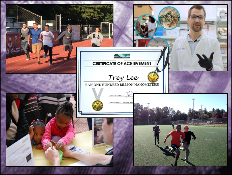
I have four items about work that will be presented at SIGGRAPH 2018, First up, something about ‘redirected walking’ from a June 18, 2018 Association for Computing Machinery news release on EurekAlert,

CHICAGO–In the burgeoning world of virtual reality (VR) technology, it remains a challenge to provide users with a realistic perception of infinite space and natural walking capabilities in the virtual environment. A team of computer scientists has introduced a new approach to address this problem by leveraging a natural human phenomenon: eye blinks.

All humans are functionally blind for about 10 percent of the time under normal circumstances due to eye blinks and saccades, a rapid movement of the eye between two points or objects. Eye blinks are a common and natural cause of so-called “change blindness,” which indicates the inability for humans to notice changes to visual scenes. Zeroing in on eye blinks and change blindness, the team has devised a novel computational system that effectively redirects the user in the virtual environment during these natural instances, all with undetectable camera movements to deliver orientation redirection.

“Previous RDW [redirected walking] techniques apply rotations continuously while the user is walking. But the amount of unnoticeable rotations is limited,” notes Eike Langbehn, lead author of the research and doctoral candidate at the University of Hamburg. “That’s why an orthogonal approach is needed–we add some additional rotations when the user is not focused on the visuals. When we learned that humans are functionally blind for some time due to blinks, we thought, ‘Why don’t we do the redirection during eye blinks?'”

Human eye blinks occur approximately 10 to 20 times per minute, about every 4 to 19 seconds. Leveraging this window of opportunity–where humans are unable to detect major motion changes while in a virtual environment–the researchers devised an approach to synchronize a computer graphics rendering system with this visual process, and introduce any useful motion changes in virtual scenes to enhance users’ overall VR experience.

The researchers’ experiments revealed that imperceptible camera rotations of 2 to 5 degrees and translations of 4 to 9 cm of the user’s viewpoint are possible during a blink without users even noticing. They tracked test participants’ eye blinks by an eye tracker in a VR head-mounted display. In a confirmatory study, the team validated that participants could not reliably detect in which of two eye blinks their viewpoint was manipulated while walking a VR curved path. The tests relied on unconscious natural eye blinking, but the researchers say redirection during blinking could be carried out consciously. Since users can consciously blink multiple times a day without much effort, eye blinks provide great potential to be used as an intentional trigger in their approach.

The team will present their work at SIGGRAPH 2018, held 12-16 August in Vancouver, British Columbia. The annual conference and exhibition showcases the world’s leading professionals, academics, and creative minds at the forefront of computer graphics and interactive techniques.

“RDW is a big challenge since current techniques still need too much space to enable unlimited walking in VR,” notes Langbehn. “Our work might contribute to a reduction of space since we found out that unnoticeable rotations of up to five degrees are possible during blinks. This means we can improve the performance of RDW by approximately 50 percent.”

The team’s results could be used in combination with other VR research, such as novel steering algorithms, improved path prediction, and rotations during saccades, to name a few. Down the road, such techniques could some day enable consumer VR users to virtually walk beyond their living room.

Langbehn collaborated on the work with Frank Steinicke of University of Hamburg, Markus Lappe of University of Muenster, Gregory F. Welch of University of Central Florida, and Gerd Bruder, also of University of Central Florida. For the full paper and video, visit the team’s project page.

###

About ACM, ACM SIGGRAPH, and SIGGRAPH 2018

ACM, the Association for Computing Machinery, is the world’s largest educational and scientific computing society, uniting educators, researchers, and professionals to inspire dialogue, share resources, and address the field’s challenges. ACM SIGGRAPH is a special interest group within ACM that serves as an interdisciplinary community for members in research, technology, and applications in computer graphics and interactive techniques. SIGGRAPH is the world’s leading annual interdisciplinary educational experience showcasing the latest in computer graphics and interactive techniques. SIGGRAPH 2018, marking the 45th annual conference hosted by ACM SIGGRAPH, will take place from 12-16 August at the Vancouver Convention Centre in Vancouver, B.C.

They have provided an image illustrating what they mean (I don’t find it especially informative),

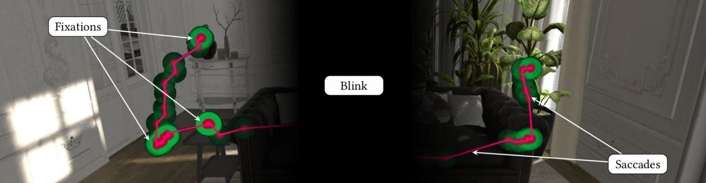
Caption: The viewing behavior of a virtual reality user, including fixations (in green) and saccades (in red). A blink fully suppresses visual perception. Credit: Eike Langbehn

Next up (2), there’s Disney Corporation’s first virtual reality (VR) short, from a July 19, 2018  Association for Computing Machinery news release on EurekAlert,

Walt Disney Animation Studios will debut its first ever virtual reality short film at SIGGRAPH 2018, and the hope is viewers will walk away feeling connected to the characters as equally as they will with the VR technology involved in making the film.

Cycles, an experimental film directed by Jeff Gipson, centers around the true meaning of creating a home and the life it holds inside its walls. The idea for the film is personal, inspired by Gipson’s childhood spending time with his grandparents and creating memories in their home, and later, having to move them to an assisted living residence.

“Every house has a story unique to the people, the characters who live there,” says Gipson. “We wanted to create a story in this single place and be able to have the viewer witness life happening around them. It is an emotionally driven film, expressing the real ups and downs, the happy and sad moments in life.”

For Cycles, Gipson also drew from his past life as an architect, having spent several years designing skate parks, and from his passion for action sports, including freestyle BMX. In Los Angeles, where Gipson lives, it is not unusual to find homes with an empty swimming pool reserved for skating or freestyle biking. Part of the pitch for Cycles came out of Gipson’s experience riding in these empty pools and being curious about the homes attached to them, the families who lived there, and the memories they made.

SIGGRAPH attendees will have the opportunity to experience Cycles at the Immersive Pavilion, a new space for this year’s conference. The Pavilion is devoted exclusively to virtual, augmented, and mixed reality and will contain: the VR Theater, a storytelling extravaganza that is part of the Computer Animation Festival; the Vrcade, a space for VR, AR, and MR games or experiences; and the well-known Village, for showcasing large-scale projects. SIGGRAPH 2018, held 12-16 August in Vancouver, British Columbia, is an annual gathering that showcases the world’s leading professionals, academics, and creative minds at the forefront of computer graphics and interactive techniques.

The production team completed Cycles in four months with about 50 collaborators as part of a professional development program at the studio. A key difference in VR filmmaking includes getting creative with how to translate a story to the VR “screen.” Pre-visualizing the narrative, for one, was a challenge. Rather than traditional storyboarding, Gipson and his team instead used a mix of Quill VR painting techniques and motion capture to “storyboard” Cycles, incorporating painters and artists to generate sculptures or 3D models of characters early on and draw scenes for the VR space. The creators also got innovative with the use of light and color saturation in scenes to help guide the user’s eyes during the film.

“What’s cool for VR is that we are really on the edge of trying to figure out what it is and how to tell stories in this new medium,” says Gipson. “In VR, you can look anywhere and really be transported to a different world, experience it from different angles, and see every detail. We want people watching to feel alive and feel emotion, and give them a true cinematic experience.”

This is Gipson’s VR directorial debut. He joined Walt Disney Animation Studios in 2013, serving as a lighting artist on Disney favorites like Frozen, Zootopia, and Moana. Of getting to direct the studio’s first VR short, he says, “VR is an amazing technology and a lot of times the technology is what is really celebrated. We hope more and more people begin to see the emotional weight of VR films, and with Cycles in particular, we hope they will feel the emotions we aimed to convey with our story.”

Apparently this is a still from the ‘short’,

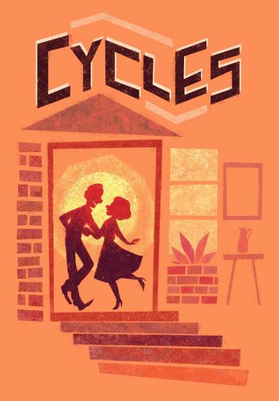
Caption: Disney Animation Studios will present ‘Cycles’ , its first virtual reality (VR) short, at ACM SIGGRAPH 2018. Credit: Disney Animation Studios

There’s also something (3) from Google as described in a July 26, 2018 Association of Computing Machinery news release on EurekAlert,

Google has unveiled a new virtual reality (VR) immersive experience based on a novel system that captures and renders high-quality, realistic images from the real world using light fields. Created by a team of leading researchers at Google, Welcome to Light Fields is the tech giant’s splash into the nascent arena of light fields VR experiences, an exciting corner of VR video technology gaining traction for its promise to deliver extremely high-quality imagery and experiences in the virtual world.

Google released Welcome to Light Fields earlier this year as a free app on Steam VR for HTC Vive, Oculus Rift, and Windows Mixed Reality headsets. The creators will demonstrate the VR experience at SIGGRAPH 2018, in the Immersive Pavilion, a new space for this year’s conference. The Pavilion is devoted exclusively to virtual, augmented, and mixed reality and will contain: the Vrcade, a space for VR, AR, and MR games or experiences; the VR Theater, a storytelling extravaganza that is part of the Computer Animation Festival; and the well-known Village, for showcasing large-scale projects. SIGGRAPH 2018, held 12-16 August in Vancouver, British Columbia, is an annual gathering that showcases the world’s leading professionals, academics, and creative minds at the forefront of computer graphics and interactive techniques.

Destinations in Welcome to Light Fields include NASA’s Space Shuttle Discovery, delivering to viewers an astronaut’s view inside the flight deck, which has never been open to the public; the pristine teak and mahogany interiors of the Gamble House, an architectural treasure in Pasadena, CA; and the glorious St. Stephen’s Church in Granada Hills, CA, home to a stunning wall of more than 14,000 pieces of glimmering stained glass.

“I love that light fields in VR can teleport you to exotic places in the real world, and truly make you believe you are there,” says Ryan Overbeck, software engineer at Google who co-led the project. “To me, this is magic.”

To bring this experience to life, Overbeck worked with a team that included Paul Debevec, senior staff engineer at Google, who managed the project and led the hardware piece with engineers Xueming Yu, Jay Busch, and Graham Fyffe. With Overbeck, Daniel Erickson and Daniel Evangelakos focused on the software end. The researchers designed a comprehensive system for capturing and rendering high-quality, spherical light field still images from footage captured in the real world. They developed two easy-to-use light field camera rigs, based on the GoPro Hero4action sports camera, that efficiently capture thousands of images on the surface of a sphere. Those images were then passed through a cloud-based light-field-processing pipeline.

Among other things, explains Overbeck, “The processing pipeline uses computer vision to place the images in 3D and generate depth maps, and we use a modified version of our vp9 video codec

to compress the light field data down to a manageable size.” To render a light field dataset, he notes, the team used a rendering algorithm that blends between the thousands of light field images in real-time.

The team relied on Google’s talented pool of engineers in computer vision, graphics, video compression, and machine learning to overcome the unique challenges posed in light fields technology. They also collaborated closely with the WebM team (who make the vp9 video codec) to develop the high-quality light field compression format incorporated into their system, and leaned heavily on the expertise of the Jump VR team to help pose the images and generate depth maps. (Jump is Google’s professional VR system for achieving 3D-360 video production at scale.)

Indeed, with Welcome to Light Fields, the Google team is demonstrating the potential and promise of light field VR technology, showcasing the technology’s ability to provide a truly immersive experience with a level of unmatched realism. Though light fields technology has been researched and explored in computer graphics for more than 30 years, practical systems for actually delivering high-quality light field experiences has not yet been possible.

Part of the team’s motivation behind creating this VR light field experience is to invigorate the nascent field.

“Welcome to Light Fields proves that it is now possible to make a compelling light field VR viewer that runs on consumer-grade hardware, and we hope that this knowledge will encourage others to get involved with building light field technology and media,” says Overbeck. “We understand that in order to eventually make compelling consumer products based on light fields, we need a thriving light field ecosystem. We need open light field codecs, we need artists creating beautiful light field imagery, and we need people using VR in order to engage with light fields.”

I don’t really understand why this image, which looks like something belongs on advertising material, would be chosen to accompany a news release on a science-based distribution outlet,

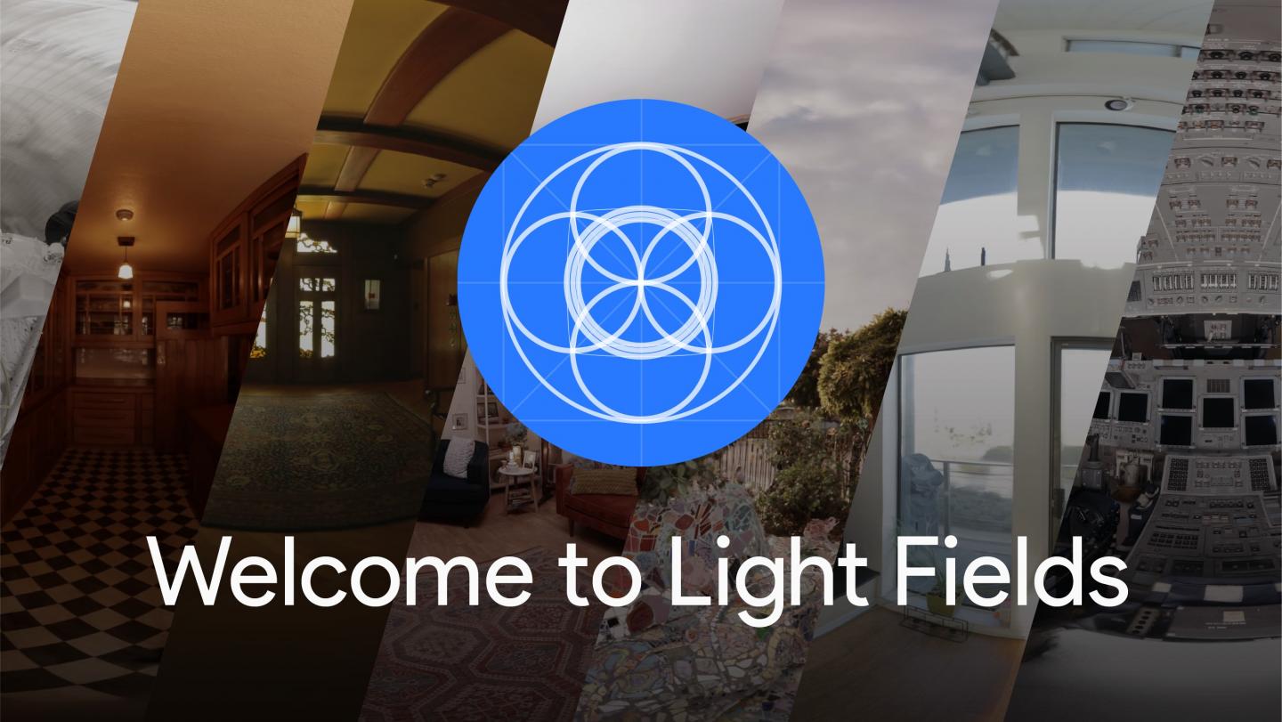
Caption: A team of leading researchers at Google, will unveil the new immersive virtual reality (VR) experience “Welcome to Lightfields” at ACM SIGGRAPH 2018. Credit: Image courtesy of Google/Overbeck

Finally (4), ‘synthesizing realistic sounds’ is announced in an Aug. 6, 2018 Stanford University (US) news release (also on EurekAlert) by Taylor Kubota,

Advances in computer-generated imagery have brought vivid, realistic animations to life, but the sounds associated with what we see simulated on screen, such as two objects colliding, are often recordings. Now researchers at Stanford University have developed a system that automatically renders accurate sounds for a wide variety of animated phenomena.

“There’s been a Holy Grail in computing of being able to simulate reality for humans. We can animate scenes and render them visually with physics and computer graphics, but, as for sounds, they are usually made up,” said Doug James, professor of computer science at Stanford University. “Currently there exists no way to generate realistic synchronized sounds for complex animated content, such as splashing water or colliding objects, automatically. This fills that void.”

The researchers will present their work on this sound synthesis system as part of ACM SIGGRAPH 2018, the leading conference on computer graphics and interactive techniques. In addition to enlivening movies and virtual reality worlds, this system could also help engineering companies prototype how products would sound before being physically produced, and hopefully encourage designs that are quieter and less irritating, the researchers said.

“I’ve spent years trying to solve partial differential equations – which govern how sound propagates – by hand,” said Jui-Hsien Wang, a graduate student in James’ lab and in the Institute for Computational and Mathematical Engineering (ICME), and lead author of the paper. “This is actually a place where you don’t just solve the equation but you can actually hear it once you’ve done it. That’s really exciting to me and it’s fun.”

Predicting sound

Informed by geometry and physical motion, the system figures out the vibrations of each object and how, like a loudspeaker, those vibrations excite sound waves. It computes the pressure waves cast off by rapidly moving and vibrating surfaces but does not replicate room acoustics. So, although it does not recreate the echoes in a grand cathedral, it can resolve detailed sounds from scenarios like a crashing cymbal, an upside-down bowl spinning to a stop, a glass filling up with water or a virtual character talking into a megaphone.

Most sounds associated with animations rely on pre-recorded clips, which require vast manual effort to synchronize with the action on-screen. These clips are also restricted to noises that exist – they can’t predict anything new. Other systems that produce and predict sounds as accurate as those of James and his team work only in special cases, or assume the geometry doesn’t deform very much. They also require a long pre-computation phase for each separate object.

“Ours is essentially just a render button with minimal pre-processing that treats all objects together in one acoustic wave simulation,” said Ante Qu, a graduate student in James’ lab and co-author of the paper.

The simulated sound that results from this method is highly detailed. It takes into account the sound waves produced by each object in an animation but also predicts how those waves bend, bounce or deaden based on their interactions with other objects and sound waves in the scene.

Challenges ahead

In its current form, the group’s process takes a while to create the finished product. But, now that they have proven this technique’s potential, they can focus on performance optimizations, such as implementing their method on parallel GPU hardware, that should make it drastically faster.

And, even in its current state, the results are worth the wait.

“The first water sounds we generated with the system were among the best ones we had simulated – and water is a huge challenge in computer-generated sound,” said James. “We thought we might get a little improvement, but it is dramatically better than previous approaches even right out of the box. It was really striking.”

Although the group’s work has faithfully rendered sounds of various objects spinning, falling and banging into each other, more complex objects and interactions – like the reverberating tones of a Stradivarius violin – remain difficult to model realistically. That, the group said, will have to wait for a future solution.

Timothy Langlois of Adobe Research is a co-author of this paper. This research was funded by the National Science Foundation and Adobe Research. James is also a professor, by courtesy, of music and a member of Stanford Bio-X.

Researchers Timothy Langlois, Doug L. James, Ante Qu and Jui-Hsien Wang have created a video featuring highlights of animations with sounds synthesized using the Stanford researchers’ new system.,

The researchers have also provided this image,

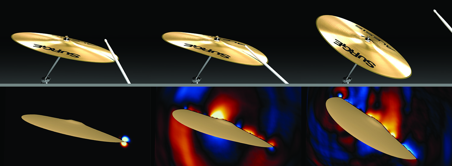
By computing pressure waves cast off by rapidly moving and vibrating surfaces – such as a cymbal – a new sound synthesis system developed by Stanford researchers can automatically render realistic sound for computer animations. (Image credit: Timothy Langlois, Doug L. James, Ante Qu and Jui-Hsien Wang)

It does seem like we’re synthesizing the world around us, eh?

The SIGGRAPH 2018 art gallery

Here’s what SIGGRAPH had to say about its 2018 art gallery in Vancouver and the themes for the conference and the gallery (from a May 18, 2018 Associating for Computing Machinery news release on globalnewswire.com (also on this 2018 SIGGRAPH webpage),

SIGGRAPH 2018, the world’s leading showcase of digital art created using computer graphics and interactive techniques, will present a special Art Gallery, entitled “Origins,” and historic Art Papers in Vancouver, B.C. The 45th SIGGRAPH conference will take place 12–16 August at the Vancouver Convention Centre. The programs will also honor the generations of creators that have come before through a special, 50th anniversary edition of the Leonard journal. To register for the conference, visit S2018.SIGGRAPH.ORG.

The SIGGRAPH 2018 ART GALLERY is a curated exhibition, conceived as a dialogical space that enables the viewer to reflect on man’s diverse cultural values and rituals through contemporary creative practices. Building upon an exciting and eclectic selection of creative practices mediated through technologies that represent the sophistication of our times, the SIGGRAPH 2018 Art Gallery will embrace the narratives of the indigenous communities based near Vancouver and throughout Canada as a source of inspiration. The exhibition will feature contemporary media artworks, art pieces by indigenous communities, and other traces of technologically mediated Ludic practices.

Andrés Burbano, SIGGRAPH 2018 Art Gallery chair and professor at Universidad de los Andes, said, “The Art Gallery aims to articulate myth and technology, science and art, the deep past and the computational present, and will coalesce around a theme of ‘Origins.’ Media and technological creative expressions will explore principles such as the origins of the cosmos, the origins of life, the origins of human presence, the origins of the occupation of territories in the Americas, and the origins of people living in the vast territories of the Arctic.”

He continued, “The venue [in Vancouver] hopes to rekindle the original spark that ignited the collaborative spirit of the SIGGRAPH community of engineers, scientists, and artists, who came together to create the very first conference in the early 1970s.”

Highlights from the 2018 Art Gallery include:

Transformation Mask (Canada) [Technology Based]
Shawn Hunt, independent; and Microsoft Garage: Andy Klein, Robert Butterworth, Jonathan Cobb, Jeremy Kersey, Stacey Mulcahy, Brendan O’Rourke, Brent Silk, and Julia Taylor-Hell, Microsoft Vancouver

TRANSFORMATION MASK is an interactive installation that features the Microsoft HoloLens. It utilizes electronics and mechanical engineering to express a physical and digital transformation. Participants are immersed in spatial sounds and holographic visuals.

Somnium (U.S.) [Science Based]
Marko Peljhan, Danny Bazo, and Karl Yerkes, University of California, Santa Barbara

Somnium is a cybernetic installation that provides visitors with the ability to sensorily, cognitively, and emotionally contemplate and experience exoplanetary discoveries, their macro and micro dimensions, and the potential for life in our Galaxy. Some might call it “space telescope.”

Ernest Edmonds Retrospective – Art Systems 1968-2018 (United Kingdom) [History Based]
Ernest Edmonds, De Montfort University

Celebrating one of the pioneers of computer graphics-based art since the early 1970s, this Ernest Edmonds career retrospective will showcase snapshots of Edmonds’ work as it developed over the years. With one piece from each decade, the retrospective will also demonstrate how vital the Leonardo journal has been throughout the 50-year journey.

In addition to the works above, the Art Gallery will feature pieces from notable female artists Ozge Samanci, Ruth West, and Nicole L’Hullier. For more information about the Edmonds retrospective, read THIS POST ON THE ACM SIGGRAPH BLOG.

The SIGGRAPH 2018 ART PAPERS program is designed to feature research from artists, scientists, theorists, technologists, historians, and more in one of four categories: project description, theory/criticism, methods, or history. The chosen work was selected by an international jury of scholars, artists, and immersive technology developers.

To celebrate the 50th anniversary of LEONARDO (MIT Press), and 10 years of its annual SIGGRAPH issue, SIGGRAPH 2018 is pleased to announce a special anniversary edition of the journal, which will feature the 2018 art papers. For 50 years, Leonardo has been the definitive publication for artist-academics. To learn more about the relationship between SIGGRAPH and the journal, listen to THIS EPISODE OF THE SIGGRAPH SPOTLIGHT PODCAST.

“In order to encourage a wider range of topics, we introduced a new submission type, short papers. This enabled us to accept more content than in previous years. Additionally, for the first time, we will introduce sessions that integrate the Art Gallery artist talks with Art Papers talks, promoting richer connections between these two creative communities,” said Angus Forbes, SIGGRAPH 2018 Art Papers chair and professor at University of California, Santa Cruz.

Art Papers highlights include:

Alienating the Familiar with CGI: A Recipe for Making a Full CGI Art House Animated Feature [Long]
Alex Counsell and Paul Charisse, University of Portsmouth

This paper explores the process of making and funding an art house feature film using full CGI in a marketplace where this has never been attempted. It explores cutting-edge technology and production approaches, as well as routes to successful fundraising.

Augmented Fauna and Glass Mutations: A Dialogue Between Material and Technique in Glassblowing and 3D Printing [Long]
Tobias Klein, City University of Hong Kong

The two presented artworks, “Augmented Fauna” and “Glass Mutations,” were created during an artist residence at the PILCHUCK GLASS SCHOOL. They are examples of the qualities and methods established through a synthesis between digital workflows and traditional craft processes and thus formulate the notion of digital craftsmanship.

Inhabitat: An Imaginary Ecosystem in a Children’s Science Museum [Short]
Graham Wakefield, York University, and Haru Hyunkyung Ji, OCAD University

“Inhabitat” is a mixed reality artwork in which participants become part of an imaginary ecology through three simultaneous perspectives of scale and agency; three distinct ways to see with other eyes. This imaginary world was exhibited at a children’s science museum for five months, using an interactive projection-augmented sculpture, a large screen and speaker array, and a virtual reality head-mounted display.

What’s the what?

My father used to say that and I always assumed it meant summarize the high points, if you need to, and get to the point—fast. In that spirit, I am both fascinated and mildly appalled. The virtual, mixed, and augmented reality technologies, as well as, the others being featured at SIGGRAPH 2018 are wondrous in many ways but it seems we are coming ever closer to a world where we no longer interact with nature or other humans directly. (see my August 10, 2018 posting about the ‘extinction of experience’ for research that encourages more direct interaction with nature) I realize that SIGGRAPH is intended as a primarily technical experience but I think a little more content questioning these technologies and their applications (social implications) might be in order. That’s often the artist’s role but I can’t see anything in the art gallery descriptions that hint at any sort of fundamental critique.

My name is Steve and I’m a sub auroral ion drift

Photo: The Aurora Named STEVE Couresty: NASA Goddard

That stunning image is one of a series, many of which were taken by amateur photographers as noted in a March 14, 2018 US National Aeronautics and Space Agency (NASA)/Goddard Space Flight Center news release (also on EurekAlert) by Kasha Patel about how STEVE was discovered,

Notanee Bourassa knew that what he was seeing in the night sky was not normal. Bourassa, an IT technician in Regina, Canada, trekked outside of his home on July 25, 2016, around midnight with his two younger children to show them a beautiful moving light display in the sky — an aurora borealis. He often sky gazes until the early hours of the morning to photograph the aurora with his Nikon camera, but this was his first expedition with his children. When a thin purple ribbon of light appeared and starting glowing, Bourassa immediately snapped pictures until the light particles disappeared 20 minutes later. Having watched the northern lights for almost 30 years since he was a teenager, he knew this wasn’t an aurora. It was something else.

From 2015 to 2016, citizen scientists — people like Bourassa who are excited about a science field but don’t necessarily have a formal educational background — shared 30 reports of these mysterious lights in online forums and with a team of scientists that run a project called Aurorasaurus. The citizen science project, funded by NASA and the National Science Foundation, tracks the aurora borealis through user-submitted reports and tweets.

The Aurorasaurus team, led by Liz MacDonald, a space scientist at NASA’s Goddard Space Flight Center in Greenbelt, Maryland, conferred to determine the identity of this mysterious phenomenon. MacDonald and her colleague Eric Donovan at the University of Calgary in Canada talked with the main contributors of these images, amateur photographers in a Facebook group called Alberta Aurora Chasers, which included Bourassa and lead administrator Chris Ratzlaff. Ratzlaff gave the phenomenon a fun, new name, Steve, and it stuck.

But people still didn’t know what it was.

Scientists’ understanding of Steve changed that night Bourassa snapped his pictures. Bourassa wasn’t the only one observing Steve. Ground-based cameras called all-sky cameras, run by the University of Calgary and University of California, Berkeley, took pictures of large areas of the sky and captured Steve and the auroral display far to the north. From space, ESA’s (the European Space Agency) Swarm satellite just happened to be passing over the exact area at the same time and documented Steve.

For the first time, scientists had ground and satellite views of Steve. Scientists have now learned, despite its ordinary name, that Steve may be an extraordinary puzzle piece in painting a better picture of how Earth’s magnetic fields function and interact with charged particles in space. The findings are published in a study released today in Science Advances.

“This is a light display that we can observe over thousands of kilometers from the ground,” said MacDonald. “It corresponds to something happening way out in space. Gathering more data points on STEVE will help us understand more about its behavior and its influence on space weather.”

The study highlights one key quality of Steve: Steve is not a normal aurora. Auroras occur globally in an oval shape, last hours and appear primarily in greens, blues and reds. Citizen science reports showed Steve is purple with a green picket fence structure that waves. It is a line with a beginning and end. People have observed Steve for 20 minutes to 1 hour before it disappears.

If anything, auroras and Steve are different flavors of an ice cream, said MacDonald. They are both created in generally the same way: Charged particles from the Sun interact with Earth’s magnetic field lines.

The uniqueness of Steve is in the details. While Steve goes through the same large-scale creation process as an aurora, it travels along different magnetic field lines than the aurora. All-sky cameras showed that Steve appears at much lower latitudes. That means the charged particles that create Steve connect to magnetic field lines that are closer to Earth’s equator, hence why Steve is often seen in southern Canada.

Perhaps the biggest surprise about Steve appeared in the satellite data. The data showed that Steve comprises a fast moving stream of extremely hot particles called a sub auroral ion drift, or SAID. Scientists have studied SAIDs since the 1970s but never knew there was an accompanying visual effect. The Swarm satellite recorded information on the charged particles’ speeds and temperatures, but does not have an imager aboard.

“People have studied a lot of SAIDs, but we never knew it had a visible light. Now our cameras are sensitive enough to pick it up and people’s eyes and intellect were critical in noticing its importance,” said Donovan, a co-author of the study. Donovan led the all-sky camera network and his Calgary colleagues lead the electric field instruments on the Swarm satellite.

Steve is an important discovery because of its location in the sub auroral zone, an area of lower latitude than where most auroras appear that is not well researched. For one, with this discovery, scientists now know there are unknown chemical processes taking place in the sub auroral zone that can lead to this light emission.

Second, Steve consistently appears in the presence of auroras, which usually occur at a higher latitude area called the auroral zone. That means there is something happening in near-Earth space that leads to both an aurora and Steve. Steve might be the only visual clue that exists to show a chemical or physical connection between the higher latitude auroral zone and lower latitude sub auroral zone, said MacDonald.

“Steve can help us understand how the chemical and physical processes in Earth’s upper atmosphere can sometimes have local noticeable effects in lower parts of Earth’s atmosphere,” said MacDonald. “This provides good insight on how Earth’s system works as a whole.”

The team can learn a lot about Steve with additional ground and satellite reports, but recording Steve from the ground and space simultaneously is a rare occurrence. Each Swarm satellite orbits Earth every 90 minutes and Steve only lasts up to an hour in a specific area. If the satellite misses Steve as it circles Earth, Steve will probably be gone by the time that same satellite crosses the spot again.

In the end, capturing Steve becomes a game of perseverance and probability.

“It is my hope that with our timely reporting of sightings, researchers can study the data so we can together unravel the mystery of Steve’s origin, creation, physics and sporadic nature,” said Bourassa. “This is exciting because the more I learn about it, the more questions I have.”

As for the name “Steve” given by the citizen scientists? The team is keeping it as an homage to its initial name and discoverers. But now it is STEVE, short for Strong Thermal Emission Velocity Enhancement.

Other collaborators on this work are: the University of Calgary, New Mexico Consortium, Boston University, Lancaster University, Athabasca University, Los Alamos National Laboratory and the Alberta Aurora Chasers Facebook group.

If you live in an area where you may see STEVE or an aurora, submit your pictures and reports to Aurorasaurus through aurorasaurus.org or the free iOS and Android mobile apps. To learn how to spot STEVE, click here.

There is a video with MacDonald describing the work and featuring more images,

Katherine Kornei’s March 14, 2018 article for sciencemag.org adds more detail about the work,

Citizen scientists first began posting about Steve on social media several years ago. Across New Zealand, Canada, the United States, and the United Kingdom, they reported an unusual sight in the night sky: a purplish line that arced across the heavens for about an hour at a time, visible at lower latitudes than classical aurorae, mostly in the spring and fall. … “It’s similar to a contrail but doesn’t disperse,” says Notanee Bourassa, an aurora photographer in Saskatchewan province in Canada [Regina as mentioned in the news release is the capital of the province of Saskatchewan].

Traditional aurorae are often green, because oxygen atoms present in Earth’s atmosphere emit that color light when they’re bombarded by charged particles trapped in Earth’s magnetic field. They also appear as a diffuse glow—rather than a distinct line—on the northern or southern horizon. Without a scientific theory to explain the new sight, a group of citizen scientists led by aurora enthusiast Chris Ratzlaff of Canada’s Alberta province [usually referred to as Canada’s province of Alberta or simply, the province of Alberta] playfully dubbed it Steve, after a line in the 2006 children’s movie Over the Hedge.

Aurorae have been studied for decades, but people may have missed Steve because their cameras weren’t sensitive enough, says Elizabeth MacDonald, a space physicist at NASA Goddard Space Flight Center in Greenbelt, Maryland, and leader of the new research. MacDonald and her team have used data from a European satellite called Swarm-A to study Steve in its native environment, about 200 kilometers up in the atmosphere. Swarm-A’s instruments revealed that the charged particles in Steve had a temperature of about 6000°C, “impressively hot” compared with the nearby atmosphere, MacDonald says. And those ions were flowing from east to west at nearly 6 kilometers per second, …

Here’s a link to and a citation for the paper,

New science in plain sight: Citizen scientists lead to the discovery of optical structure in the upper atmosphere by Elizabeth A. MacDonald, Eric Donovan, Yukitoshi Nishimura, Nathan A. Case, D. Megan Gillies, Bea Gallardo-Lacourt, William E. Archer, Emma L. Spanswick, Notanee Bourassa, Martin Connors, Matthew Heavner, Brian Jackel, Burcu Kosar, David J. Knudsen, Chris Ratzlaff, and Ian Schofield. Science Advances 14 Mar 2018:
Vol. 4, no. 3, eaaq0030 DOI: 10.1126/sciadv.aaq0030

This paper is open access. You’ll note that Notanee Bourassa is listed as an author. For more about Bourassa, there’s his Twitter feed (@DJHardwired) and his YouTube Channel. BTW, his Twitter bio notes that he’s “Recently heartbroken,” as well as, “Seasoned human male. Expert storm chaser, aurora photographer, drone flyer and on-air FM radio DJ.” Make of that what you will.

Smart paint that ‘talks’ to canes for better safety crossing the street

It would be nice if they had some video of people navigating with the help of this ‘smart’ paint. Perhaps one day. Meanwhile, Adele Peters in her March 7, 2018 article for Fast Company provides a vivid description of how a sight-impaired or blind person could navigate more safely and easily,

The crosswalk on a road in front of the Ohio State School for the Blind looks like one that might be found at any intersection. But the white stripes at the edges are made with “smart paint”–and if a student who is visually impaired crosses while using a cane with a new smart tip, the cane will vibrate when it touches the lines.

The paint uses rare-earth nanocrystals that can emit a unique light signature, which a sensor added to the tip of a cane can activate and then read. “If you pulse a laser or LED into these materials, they’ll pulse back at you at a very specific frequency,” says Josh Collins, chief technology officer at Intelligent Materials [sic], the company that manufacturers the oxides that can be added to paint.

While digging down for more information, this February 12, 2018 article by Ben Levine for Government Technology Magazine was unearthed (Note: Links have been removed),

In this installment of the Innovation of the Month series (read last month’s story here), we explore the use of smart technologies to help blind and visually impaired people better navigate the world around them. A team at Ohio State University has been working on a “smart paint” application to do just that.

MetroLab’s Executive Director Ben Levine sat down with John Lannutti, professor of materials science engineering at Ohio State University; Mary Ball-Swartwout, orientation and mobility specialist at the Ohio State School for the Blind; and Josh Collins, chief technology officer at Intelligent Material to learn more.

John Lannutti (OSU): The goal of “smart paint for networked smart cities” is to assist people who are blind and visually impaired by implementing a “smart paint” technology that provides accurate location services. You might think, “Can’t GPS do that?” But, surprisingly, current GPS-based solutions actually cannot tell whether somebody is walking on the sidewalk or down the middle of the street. Meanwhile, modern urban intersections are becoming increasingly complex. That means that finding a crosswalk, aligning to cross and maintaining a consistent crossing direction while in motion can be challenging for people who are visually impaired.

And of course, crosswalks aren’t the only challenge. For example, our current mapping technologies are unable to provide the exact location of a building’s entrance. We have a technology solution to those challenges. Smart paint is created by adding exotic light-converting oxides to standard road paints. The paint is detected using a “smart cane,” a modified white cane that detects the smart paint and enables portal-to-portal guidance. The smart cane can also be used to notify vehicles — including autonomous vehicles — of a user’s presence in a crosswalk.

As part of this project, we have a whole team of educational, city and industrial partners, including:

Educational partners: 

  • Ohio State School for the Blind — testing and implementation of smart paint technology in Columbus involving both students and adults
  • Western Michigan University — implementation of smart paint technology with travelers who are blind and visually impaired to maximize orientation and mobility
  • Mississippi State University — the impacts of smart paint technology on mobility and employment for people who are blind and visually impaired

City partners:  

  • Columbus Smart Cities Initiative — rollout of smart paint within Columbus and the paint’s interaction with the Integrated Data Exchange (IDE), a cloud-based platform that dynamically collects user data to show technological impact
  • The city of Tampa, Fla. — rollout of smart paint at the Lighthouse for the Blind
  • The Hillsborough Area Transit Regional Authority, Hillsborough County, Fla. — integration of smart paint with existing bus lines to enable precise location determination
  • The American Council of the Blind — implementation of smart paint with the annual American Council of the Blind convention
  • MetroLab Network — smart paint implementation in city-university partnerships

Industrial collaborators:  

  • Intelligent Material — manufactures and supplies the unique light-converting oxides that make the paint “smart”
  • Crown Technology — paint manufacturing, product evaluation and technical support
  • SRI International — design and manufacturing of the “smart” white cane hardware

Levine: Can you describe what this project focused on and what motivated you to address this particular challenge?

Lannutti: We have been working with Intelligent Material in integrating light-converting oxides into polymeric matrices for specific applications for several years. Intelligent Material supplies these oxides for highly specialized applications across a variety of industries, and has deep experience in filtering and processing the resulting optical outputs. They were already looking at using this technology for automotive applications when the idea to develop applications for people who are blind was introduced. We were extremely fortunate to have the Ohio State School for the Blind (OSSB) right here in Columbus and even more fortunate to have interested collaborators there who have helped us at every step of the way. They even have a room filled with previous white cane technologies; we used those to better understand what works and what doesn’t, helping refine our own product. At about this same time, the National Science Foundation released a call for Smart and Connected Communities proposals, which gave us both a goal and a “home” for this idea.

Levine: How will the tools developed in this project impact planning and the built environment?

Ball-Swartwout: One of the great things about smart paint is that it can be added to the built environment easily at little extra cost. We expect that once smart paint is widely adopted, most sighted users will not notice much difference as smart paint is not visually different from regular road paint. Some intersections might need to have more paint features that enable smart white cane-guided entry from the sidewalk into the crosswalk. Paint that tells users that they have reached their destination may become visible as horizontal stripes along modern sidewalks. These paints could be either gray or black or even invisible to sighted pedestrians, but would still be detectable by “smart” white canes to tell users that they have arrived at their destination.

Levine: Can you tell us about the new technologies that are associated with this project? Can you talk about the status quo versus your vision for the future?

Collins: Beyond converting ceramics in paint, placing a highly sensitive excitation source and detector package at the tip of a moving white cane is truly novel. Also challenging is powering this package using minimal battery weight to decrease the likelihood of wrist and upper neck fatigue.

The status quo is that the travel of citizens who are blind and visually impaired can be unpredictable. They need better technologies for routine travel and especially for travel to any new destinations. In addition, we anticipate that this technology could assist in the travel of people who have a variety of physical and cognitive impairments.

Our vision for the future of this technology is that it will be widespread and utilized constantly. Outside the U.S., Japan and Europe have integrated relatively expensive technologies into streets and sidewalks, and we see smart paint replacing that very quickly. Because the “pain” of installing smart paint is very small, we believe that grass-roots pressure will enable rapid introduction of this technology.

Levine: What was the most surprising thing you learned during this process?

Lannutti: In my mind, the most surprising thing was discovering that sound was not necessarily the best means of guiding users who are blind. This is a bias on the part of sighted individuals as we are used to beeping and buzzing noises that guide or inform us throughout our day. Pedestrians who are blind, on the other hand, need to constantly listen to aspects of their environment to successfully navigate it. For example, listening to traffic noise is extremely important to them as a means of avoiding danger. People who are blind or visually impaired cannot see but need to hear their environment. So we had to dial back our expectations regarding the utility of sound. Instead, we now focus on vibration along the white cane as a means of alerting the user.

If those interested, Levine’s article is well worth reading in its entirety.

Thankfully they’ve added some information to the website for Intelligent Material (Solutions) since I first viewed it.

There’s a bit more information on the Intelligent Material (Solutions’) YouTube video webpage,

Intelligent Material Solutions, Inc. is a privately held business headquartered in Princeton, NJ in the SRI/Sarnoff Campus, formerly RCA Labs. Our technology can be traced through scientific discoveries dating back over 50 years. We are dedicated to solving the worlds’ most challenging problems and in doing so have assembled an innovative, multi-discipliary team of leading scientists from industry and academia to ensure rapid transition from our labs to the world.

The video was published on December 6, 2017. You can find even more details at the company’s LinkedIn page.

Announcing the ‘memtransistor’

Yet another advance toward ‘brainlike’ computing (how many times have I written this or a variation thereof in the last 10 years? See: Dexter Johnson’s take on the situation at the end of this post): Northwestern University announced their latest memristor research in a February 21, 2018 news item on Nanowerk,

Computer algorithms might be performing brain-like functions, such as facial recognition and language translation, but the computers themselves have yet to operate like brains.

“Computers have separate processing and memory storage units, whereas the brain uses neurons to perform both functions,” said Northwestern University’s Mark C. Hersam. “Neural networks can achieve complicated computation with significantly lower energy consumption compared to a digital computer.”

A February 21, 2018 Northwestern University news release (also on EurekAlert), which originated the news item, provides more information about the latest work from this team,

In recent years, researchers have searched for ways to make computers more neuromorphic, or brain-like, in order to perform increasingly complicated tasks with high efficiency. Now Hersam, a Walter P. Murphy Professor of Materials Science and Engineering in Northwestern’s McCormick School of Engineering, and his team are bringing the world closer to realizing this goal.

The research team has developed a novel device called a “memtransistor,” which operates much like a neuron by performing both memory and information processing. With combined characteristics of a memristor and transistor, the memtransistor also encompasses multiple terminals that operate more similarly to a neural network.

Supported by the National Institute of Standards and Technology and the National Science Foundation, the research was published online today, February 22 [2018], in Nature. Vinod K. Sangwan and Hong-Sub Lee, postdoctoral fellows advised by Hersam, served as the paper’s co-first authors.

The memtransistor builds upon work published in 2015, in which Hersam, Sangwan, and their collaborators used single-layer molybdenum disulfide (MoS2) to create a three-terminal, gate-tunable memristor for fast, reliable digital memory storage. Memristor, which is short for “memory resistors,” are resistors in a current that “remember” the voltage previously applied to them. Typical memristors are two-terminal electronic devices, which can only control one voltage channel. By transforming it into a three-terminal device, Hersam paved the way for memristors to be used in more complex electronic circuits and systems, such as neuromorphic computing.

To develop the memtransistor, Hersam’s team again used atomically thin MoS2 with well-defined grain boundaries, which influence the flow of current. Similar to the way fibers are arranged in wood, atoms are arranged into ordered domains – called “grains” – within a material. When a large voltage is applied, the grain boundaries facilitate atomic motion, causing a change in resistance.

“Because molybdenum disulfide is atomically thin, it is easily influenced by applied electric fields,” Hersam explained. “This property allows us to make a transistor. The memristor characteristics come from the fact that the defects in the material are relatively mobile, especially in the presence of grain boundaries.”

But unlike his previous memristor, which used individual, small flakes of MoS2, Hersam’s memtransistor makes use of a continuous film of polycrystalline MoS2 that comprises a large number of smaller flakes. This enabled the research team to scale up the device from one flake to many devices across an entire wafer.

“When length of the device is larger than the individual grain size, you are guaranteed to have grain boundaries in every device across the wafer,” Hersam said. “Thus, we see reproducible, gate-tunable memristive responses across large arrays of devices.”

After fabricating memtransistors uniformly across an entire wafer, Hersam’s team added additional electrical contacts. Typical transistors and Hersam’s previously developed memristor each have three terminals. In their new paper, however, the team realized a seven-terminal device, in which one terminal controls the current among the other six terminals.

“This is even more similar to neurons in the brain,” Hersam said, “because in the brain, we don’t usually have one neuron connected to only one other neuron. Instead, one neuron is connected to multiple other neurons to form a network. Our device structure allows multiple contacts, which is similar to the multiple synapses in neurons.”

Next, Hersam and his team are working to make the memtransistor faster and smaller. Hersam also plans to continue scaling up the device for manufacturing purposes.

“We believe that the memtransistor can be a foundational circuit element for new forms of neuromorphic computing,” he said. “However, making dozens of devices, as we have done in our paper, is different than making a billion, which is done with conventional transistor technology today. Thus far, we do not see any fundamental barriers that will prevent further scale up of our approach.”

The researchers have made this illustration available,

Caption: This is the memtransistor symbol overlaid on an artistic rendering of a hypothetical circuit layout in the shape of a brain. Credit; Hersam Research Group

Here’s a link to and a citation for the paper,

Multi-terminal memtransistors from polycrystalline monolayer molybdenum disulfide by Vinod K. Sangwan, Hong-Sub Lee, Hadallia Bergeron, Itamar Balla, Megan E. Beck, Kan-Sheng Chen, & Mark C. Hersam. Nature volume 554, pages 500–504 (22 February 2018 doi:10.1038/nature25747 Published online: 21 February 2018

This paper is behind a paywall.

The team’s earlier work referenced in the news release was featured here in an April 10, 2015 posting.

Dexter Johnson

From a Feb. 23, 2018 posting by Dexter Johnson on the Nanoclast blog (on the IEEE [Institute of Electrical and Electronics Engineers] website),

While this all seems promising, one of the big shortcomings in neuromorphic computing has been that it doesn’t mimic the brain in a very important way. In the brain, for every neuron there are a thousand synapses—the electrical signal sent between the neurons of the brain. This poses a problem because a transistor only has a single terminal, hardly an accommodating architecture for multiplying signals.

Now researchers at Northwestern University, led by Mark Hersam, have developed a new device that combines memristors—two-terminal non-volatile memory devices based on resistance switching—with transistors to create what Hersam and his colleagues have dubbed a “memtransistor” that performs both memory storage and information processing.

This most recent research builds on work that Hersam and his team conducted back in 2015 in which the researchers developed a three-terminal, gate-tunable memristor that operated like a kind of synapse.

While this work was recognized as mimicking the low-power computing of the human brain, critics didn’t really believe that it was acting like a neuron since it could only transmit a signal from one artificial neuron to another. This was far short of a human brain that is capable of making tens of thousands of such connections.

“Traditional memristors are two-terminal devices, whereas our memtransistors combine the non-volatility of a two-terminal memristor with the gate-tunability of a three-terminal transistor,” said Hersam to IEEE Spectrum. “Our device design accommodates additional terminals, which mimic the multiple synapses in neurons.”

Hersam believes that these unique attributes of these multi-terminal memtransistors are likely to present a range of new opportunities for non-volatile memory and neuromorphic computing.

If you have the time and the interest, Dexter’s post provides more context,

Santiago Ramón y Cajal and the butterflies of the soul

The Cajal exhibit of drawings was here in Vancouver (Canada) this last fall (2017) and I still carry the memory of that glorious experience (see my Sept. 11, 2017 posting for more about the show and associated events). It seems Cajal’s drawings had a similar response in New York city, from a January 18, 2018 article by Roberta Smith for the New York Times,

It’s not often that you look at an exhibition with the help of the very apparatus that is its subject. But so it is with “The Beautiful Brain: The Drawings of Santiago Ramón y Cajal” at the Grey Art Gallery at New York University, one of the most unusual, ravishing exhibitions of the season.

The show finished its run on March 31, 2018 and is now on its way to the Massachusetts Institute of Technology (MIT) in Boston, Massachusetts for its opening on May 3, 2018. It looks like they have an exciting lineup of events to go along with the exhibit (from MIT’s The Beautiful Brain: The Drawings of Santiago Ramón y Cajal exhibit and event page),

SUMMER PROGRAMS

ONGOING

Spotlight Tours
Explorations led by local and Spanish scientists, artists, and entrepreneurs who will share their unique perspectives on particular aspects of the exhibition. (2:00 pm on select Tuesdays and Saturdays)

Tue, May 8 – Mark Harnett, Fred and Carole Middleton Career Development Professor at MIT and McGovern Institute Investigator Sat, May 26 – Marion Boulicault, MIT Graduate Student and Neuroethics Fellow in the Center for Sensorimotor Neural Engineering Tue, June 5 – Kelsey Allen, Graduate researcher, MIT Center for Brains, Minds, and Machines Sat, Jun 23 – Francisco Martin-Martinez, Research Scientist in MIT’s Laboratory for Atomistic & Molecular Mechanics and President of the Spanish Foundation for Science and Technology Jul 21 – Alex Gomez-Marin, Principal Investigator of the Behavior of Organisms Laboratory in the Instituto de Neurociencias, Spain Tue, Jul 31– Julie Pryor, Director of Communications at the McGovern Institute for Brain Research at MIT Tue, Aug 28 – Satrajit Ghosh, Principal Research Scientist at the McGovern Institute for Brain Research at MIT, Assistant Professor in the Department of Otolaryngology at Harvard Medical School, and faculty member in the Speech and Hearing Biosciences and Technology program in the Harvard Division of Medical Sciences

Idea Hub
Drop in and explore expansion microscopy in our maker-space.

Visualizing Science Workshop
Experiential learning with micro-scale biological images. (pre-registration required)

Gallery Demonstrations
Researchers share the latest on neural anatomy, signal transmission, and modern imaging techniques.

EVENTS

Teen Science Café: Mindful Matters
MIT researchers studying the brain share their mind-blowing findings.

Neuron Paint Night
Create a painting of cerebral cortex neurons and learn about the EyeWire citizen science game.

Cerebral Cinema Series
Hear from researchers and then compare real science to depictions on the big screen.

Brainy Trivia
Test your brain power in a night of science trivia and short, snappy research talks.

Come back to see our exciting lineup for the fall!

If you don’t have a chance to see the show or if you’d like a preview, I encourage you to read Smith’s article as it has embedded several Cajal drawings and rendered them exceptionally well.

For those who like a little contemporary (and related) science with their art, there’s a March 30, 2018 Harvard Medical Schoo (HMS)l news release by Kevin Jang (also on EurekAlert), Note: All links save one have been removed,

Drawing of the cells of the chick cerebellum by Santiago Ramón y Cajal, from “Estructura de los centros nerviosos de las aves,” Madrid, circa 1905


Modern neuroscience, for all its complexity, can trace its roots directly to a series of pen-and-paper sketches rendered by Nobel laureate Santiago Ramón y Cajal in the late 19th and early 20th centuries.

His observations and drawings exposed the previously hidden composition of the brain, revealing neuronal cell bodies and delicate projections that connect individual neurons together into intricate networks.

As he explored the nervous systems of various organisms under his microscope, a natural question arose: What makes a human brain different from the brain of any other species?

At least part of the answer, Ramón y Cajal hypothesized, lay in a specific class of neuron—one found in a dazzling variety of shapes and patterns of connectivity, and present in higher proportions in the human brain than in the brains of other species. He dubbed them the “butterflies of the soul.”

Known as interneurons, these cells play critical roles in transmitting information between sensory and motor neurons, and, when defective, have been linked to diseases such as schizophrenia, autism and intellectual disability.

Despite more than a century of study, however, it remains unclear why interneurons are so diverse and what specific functions the different subtypes carry out.

Now, in a study published in the March 22 [2018] issue of Nature, researchers from Harvard Medical School, New York Genome Center, New York University and the Broad Institute of MIT and Harvard have detailed for the first time how interneurons emerge and diversify in the brain.

Using single-cell analysis—a technology that allows scientists to track cellular behavior one cell at a time—the team traced the lineage of interneurons from their earliest precursor states to their mature forms in mice. The researchers identified key genetic programs that determine the fate of developing interneurons, as well as when these programs are switched on or off.

The findings serve as a guide for efforts to shed light on interneuron function and may help inform new treatment strategies for disorders involving their dysfunction, the authors said.

“We knew more than 100 years ago that this huge diversity of morphologically interesting cells existed in the brain, but their specific individual roles in brain function are still largely unclear,” said co-senior author Gordon Fishell, HMS professor of neurobiology and a faculty member at the Stanley Center for Psychiatric Research at the Broad.

“Our study provides a road map for understanding how and when distinct interneuron subtypes develop, giving us unprecedented insight into the biology of these cells,” he said. “We can now investigate interneuron properties as they emerge, unlock how these important cells function and perhaps even intervene when they fail to develop correctly in neuropsychiatric disease.”

A hippocampal interneuron. Image: Biosciences Imaging Gp, Soton, Wellcome Trust via Creative CommonsA hippocampal interneuron. Image: Biosciences Imaging Gp, Soton, Wellcome Trust via Creative Commons

Origins and Fates

In collaboration with co-senior author Rahul Satija, core faculty member of the New York Genome Center, Fishell and colleagues analyzed brain regions in developing mice known to contain precursor cells that give rise to interneurons.

Using Drop-seq, a single-cell sequencing technique created by researchers at HMS and the Broad, the team profiled gene expression in thousands of individual cells at multiple time points.

This approach overcomes a major limitation in past research, which could analyze only the average activity of mixtures of many different cells.

In the current study, the team found that the precursor state of all interneurons had similar gene expression patterns despite originating in three separate brain regions and giving rise to 14 or more interneuron subtypes alone—a number still under debate as researchers learn more about these cells.

“Mature interneuron subtypes exhibit incredible diversity. Their morphology and patterns of connectivity and activity are so different from each other, but our results show that the first steps in their maturation are remarkably similar,” said Satija, who is also an assistant professor of biology at New York University.

“They share a common developmental trajectory at the earliest stages, but the seeds of what will cause them to diverge later—a handful of genes—are present from the beginning,” Satija said.

As they profiled cells at later stages in development, the team observed the initial emergence of four interneuron “cardinal” classes, which give rise to distinct fates. Cells were committed to these fates even in the early embryo. By developing a novel computational strategy to link precursors with adult subtypes, the researchers identified individual genes that were switched on and off when cells began to diversify.

For example, they found that the gene Mef2c—mutations of which are linked to Alzheimer’s disease, schizophrenia and neurodevelopmental disorders in humans—is an early embryonic marker for a specific interneuron subtype known as Pvalb neurons. When they deleted Mef2c in animal models, Pvalb neurons failed to develop.

These early genes likely orchestrate the execution of subsequent genetic subroutines, such as ones that guide interneuron subtypes as they migrate to different locations in the brain and ones that help form unique connection patterns with other neural cell types, the authors said.

The identification of these genes and their temporal activity now provide researchers with specific targets to investigate the precise functions of interneurons, as well as how neurons diversify in general, according to the authors.

“One of the goals of this project was to address an incredibly fascinating developmental biology question, which is how individual progenitor cells decide between different neuronal fates,” Satija said. “In addition to these early markers of interneuron divergence, we found numerous additional genes that increase in expression, many dramatically, at later time points.”

The association of some of these genes with neuropsychiatric diseases promises to provide a better understanding of these disorders and the development of therapeutic strategies to treat them, a particularly important notion given the paucity of new treatments, the authors said.

Over the past 50 years, there have been no fundamentally new classes of neuropsychiatric drugs, only newer versions of old drugs, the researchers pointed out.

“Our repertoire is no better than it was in the 1970s,” Fishell said.

“Neuropsychiatric diseases likely reflect the dysfunction of very specific cell types. Our study puts forward a clear picture of what cells to look at as we work to shed light on the mechanisms that underlie these disorders,” Fishell said. “What we will find remains to be seen, but we have new, strong hypotheses that we can now test.”

As a resource for the research community, the study data and software are open-source and freely accessible online.

A gallery of the drawings of Santiago Ramón y Cajal is currently on display in New York City, and will open at the MIT Museum in Boston in May 2018.

Christian Mayer, Christoph Hafemeister and Rachel Bandler served as co-lead authors on the study.

This work was supported by the National Institutes of Health (R01 NS074972, R01 NS081297, MH071679-12, DP2-HG-009623, F30MH114462, T32GM007308, F31NS103398), the European Molecular Biology Organization, the National Science Foundation and the Simons Foundation.

Here’s link to and a citation for the paper,

Developmental diversification of cortical inhibitory interneurons by Christian Mayer, Christoph Hafemeister, Rachel C. Bandler, Robert Machold, Renata Batista Brito, Xavier Jaglin, Kathryn Allaway, Andrew Butler, Gord Fishell, & Rahul Satija. Nature volume 555, pages 457–462 (22 March 2018) doi:10.1038/nature25999 Published: 05 March 2018

This paper is behind a paywall.

New path to viable memristor/neuristor?

I first stumbled onto memristors and the possibility of brain-like computing sometime in 2008 (around the time that R. Stanley Williams and his team at HP Labs first published the results of their research linking Dr. Leon Chua’s memristor theory to their attempts to shrink computer chips). In the almost 10 years since, scientists have worked hard to utilize memristors in the field of neuromorphic (brain-like) engineering/computing.

A January 22, 2018 news item on phys.org describes the latest work,

When it comes to processing power, the human brain just can’t be beat.

Packed within the squishy, football-sized organ are somewhere around 100 billion neurons. At any given moment, a single neuron can relay instructions to thousands of other neurons via synapses—the spaces between neurons, across which neurotransmitters are exchanged. There are more than 100 trillion synapses that mediate neuron signaling in the brain, strengthening some connections while pruning others, in a process that enables the brain to recognize patterns, remember facts, and carry out other learning tasks, at lightning speeds.

Researchers in the emerging field of “neuromorphic computing” have attempted to design computer chips that work like the human brain. Instead of carrying out computations based on binary, on/off signaling, like digital chips do today, the elements of a “brain on a chip” would work in an analog fashion, exchanging a gradient of signals, or “weights,” much like neurons that activate in various ways depending on the type and number of ions that flow across a synapse.

In this way, small neuromorphic chips could, like the brain, efficiently process millions of streams of parallel computations that are currently only possible with large banks of supercomputers. But one significant hangup on the way to such portable artificial intelligence has been the neural synapse, which has been particularly tricky to reproduce in hardware.

Now engineers at MIT [Massachusetts Institute of Technology] have designed an artificial synapse in such a way that they can precisely control the strength of an electric current flowing across it, similar to the way ions flow between neurons. The team has built a small chip with artificial synapses, made from silicon germanium. In simulations, the researchers found that the chip and its synapses could be used to recognize samples of handwriting, with 95 percent accuracy.

A January 22, 2018 MIT news release by Jennifer Chua (also on EurekAlert), which originated the news item, provides more detail about the research,

The design, published today [January 22, 2018] in the journal Nature Materials, is a major step toward building portable, low-power neuromorphic chips for use in pattern recognition and other learning tasks.

The research was led by Jeehwan Kim, the Class of 1947 Career Development Assistant Professor in the departments of Mechanical Engineering and Materials Science and Engineering, and a principal investigator in MIT’s Research Laboratory of Electronics and Microsystems Technology Laboratories. His co-authors are Shinhyun Choi (first author), Scott Tan (co-first author), Zefan Li, Yunjo Kim, Chanyeol Choi, and Hanwool Yeon of MIT, along with Pai-Yu Chen and Shimeng Yu of Arizona State University.

Too many paths

Most neuromorphic chip designs attempt to emulate the synaptic connection between neurons using two conductive layers separated by a “switching medium,” or synapse-like space. When a voltage is applied, ions should move in the switching medium to create conductive filaments, similarly to how the “weight” of a synapse changes.

But it’s been difficult to control the flow of ions in existing designs. Kim says that’s because most switching mediums, made of amorphous materials, have unlimited possible paths through which ions can travel — a bit like Pachinko, a mechanical arcade game that funnels small steel balls down through a series of pins and levers, which act to either divert or direct the balls out of the machine.

Like Pachinko, existing switching mediums contain multiple paths that make it difficult to predict where ions will make it through. Kim says that can create unwanted nonuniformity in a synapse’s performance.

“Once you apply some voltage to represent some data with your artificial neuron, you have to erase and be able to write it again in the exact same way,” Kim says. “But in an amorphous solid, when you write again, the ions go in different directions because there are lots of defects. This stream is changing, and it’s hard to control. That’s the biggest problem — nonuniformity of the artificial synapse.”

A perfect mismatch

Instead of using amorphous materials as an artificial synapse, Kim and his colleagues looked to single-crystalline silicon, a defect-free conducting material made from atoms arranged in a continuously ordered alignment. The team sought to create a precise, one-dimensional line defect, or dislocation, through the silicon, through which ions could predictably flow.

To do so, the researchers started with a wafer of silicon, resembling, at microscopic resolution, a chicken-wire pattern. They then grew a similar pattern of silicon germanium — a material also used commonly in transistors — on top of the silicon wafer. Silicon germanium’s lattice is slightly larger than that of silicon, and Kim found that together, the two perfectly mismatched materials can form a funnel-like dislocation, creating a single path through which ions can flow.

The researchers fabricated a neuromorphic chip consisting of artificial synapses made from silicon germanium, each synapse measuring about 25 nanometers across. They applied voltage to each synapse and found that all synapses exhibited more or less the same current, or flow of ions, with about a 4 percent variation between synapses — a much more uniform performance compared with synapses made from amorphous material.

They also tested a single synapse over multiple trials, applying the same voltage over 700 cycles, and found the synapse exhibited the same current, with just 1 percent variation from cycle to cycle.

“This is the most uniform device we could achieve, which is the key to demonstrating artificial neural networks,” Kim says.

Writing, recognized

As a final test, Kim’s team explored how its device would perform if it were to carry out actual learning tasks — specifically, recognizing samples of handwriting, which researchers consider to be a first practical test for neuromorphic chips. Such chips would consist of “input/hidden/output neurons,” each connected to other “neurons” via filament-based artificial synapses.

Scientists believe such stacks of neural nets can be made to “learn.” For instance, when fed an input that is a handwritten ‘1,’ with an output that labels it as ‘1,’ certain output neurons will be activated by input neurons and weights from an artificial synapse. When more examples of handwritten ‘1s’ are fed into the same chip, the same output neurons may be activated when they sense similar features between different samples of the same letter, thus “learning” in a fashion similar to what the brain does.

Kim and his colleagues ran a computer simulation of an artificial neural network consisting of three sheets of neural layers connected via two layers of artificial synapses, the properties of which they based on measurements from their actual neuromorphic chip. They fed into their simulation tens of thousands of samples from a handwritten recognition dataset commonly used by neuromorphic designers, and found that their neural network hardware recognized handwritten samples 95 percent of the time, compared to the 97 percent accuracy of existing software algorithms.

The team is in the process of fabricating a working neuromorphic chip that can carry out handwriting-recognition tasks, not in simulation but in reality. Looking beyond handwriting, Kim says the team’s artificial synapse design will enable much smaller, portable neural network devices that can perform complex computations that currently are only possible with large supercomputers.

“Ultimately we want a chip as big as a fingernail to replace one big supercomputer,” Kim says. “This opens a stepping stone to produce real artificial hardware.”

This research was supported in part by the National Science Foundation.

Here’s a link to and a citation for the paper,

SiGe epitaxial memory for neuromorphic computing with reproducible high performance based on engineered dislocations by Shinhyun Choi, Scott H. Tan, Zefan Li, Yunjo Kim, Chanyeol Choi, Pai-Yu Chen, Hanwool Yeon, Shimeng Yu, & Jeehwan Kim. Nature Materials (2018) doi:10.1038/s41563-017-0001-5 Published online: 22 January 2018

This paper is behind a paywall.

For the curious I have included a number of links to recent ‘memristor’ postings here,

January 22, 2018: Memristors at Masdar

January 3, 2018: Mott memristor

August 24, 2017: Neuristors and brainlike computing

June 28, 2017: Dr. Wei Lu and bio-inspired ‘memristor’ chips

May 2, 2017: Predicting how a memristor functions

December 30, 2016: Changing synaptic connectivity with a memristor

December 5, 2016: The memristor as computing device

November 1, 2016: The memristor as the ‘missing link’ in bioelectronic medicine?

You can find more by using ‘memristor’ as the search term in the blog search function or on the search engine of your choice.

University of Washington (state) is accelerating nanoscale research with Institute for Nano-Engineered Systems

A December 5, 2017 news item on Nanowerk announced a new research institute at the University of Washington (state),

The University of Washington [UW} has launched a new institute aimed at accelerating research at the nanoscale: the Institute for Nano-Engineered Systems, or NanoES. Housed in a new, multimillion-dollar facility on the UW’s Seattle campus, the institute will pursue impactful advancements in a variety of disciplines — including energy, materials science, computation and medicine. Yet these advancements will be at a technological scale a thousand times smaller than the width of a human hair.

The institute was launched at a reception Dec. 4 [2017] at its headquarters in the $87.8-million Nano Engineering and Sciences Building. During the event, speakers including UW officials and NanoES partners celebrated the NanoES mission to capitalize on the university’s strong record of research at the nanoscale and engage partners in industry at the onset of new projects.

A December 5, 2017 UW news release, which originated the news item, somewhat clarifies the declarations in the two excerpted paragraphs in the above,

The vision of the NanoES, which is part of the UW’s College of Engineering, is to act as a magnet for researchers in nanoscale science and engineering, with a focus on enabling industry partnership and entrepreneurship at the earliest stages of research projects. According to Karl Böhringer, director of the NanoES and a UW professor of electrical engineering and bioengineering, this unique approach will hasten the development of solutions to the field’s most pressing challenges: the manufacturing of scalable, high-yield nano-engineered systems for applications in information processing, energy, health and interconnected life.

“The University of Washington is well known for its expertise in nanoscale materials, processing, physics and biology — as well as its cutting-edge nanofabrication, characterization and testing facilities,” said Böhringer, who stepped down as director of the UW-based Washington Nanofabrication Facility to lead the NanoES. “NanoES will build on these strengths, bringing together people, tools and opportunities to develop nanoscale devices and systems.”

The centerpiece of the NanoES is its headquarters, the Nano Engineering and Sciences Building. The building houses 90,300 square feet of research and learning space, and was funded largely by the College of Engineering and Sound Transit. It contains an active learning classroom, a teaching laboratory and a 3,000-square-foot common area designed expressly to promote the sharing and exchanging of ideas. The remainder includes “incubator-style” office space and more than 40,000 square feet of flexible multipurpose laboratory and instrumentation space. The building’s location and design elements are intended to limit vibrations and electromagnetic interference so it can house sensitive experiments.

NanoES will house research in nanotechnology fields that hold promise for high impact, such as:

  • Augmented humanity, which includes technology to both aid and replace human capability in a way that joins user and machine as one – and foresees portable, wearable, implantable and networked technology for applications such as personalized medical care, among others.
  • Integrated photonics, which ranges from single-photon sensors for health care diagnostic tests to large-scale, integrated networks of photonic devices.
  • Scalable nanomanufacturing, which aims to develop low-cost, high-volume manufacturing processes. These would translate device prototypes constructed in research laboratories into system- and network-level nanomanufacturing methods for applications ranging from the 3-D printing of cell and tissue scaffolds to ultrathin solar cells.

A ribbon cutting ceremony.

Cutting the ribbon for the NanoES on Dec. 4. Left-to-right: Karl Böhringer, director of the NanoES and a UW professor of electrical engineering and bioengineering; Nena Golubovic, physical sciences director for IP Group; Mike Bragg, Dean of the UW College of Engineering; Jevne Micheau-Cunningham, deputy director of the NanoES.Kathryn Sauber/University of Washington

Collaborations with other UW-based institutions will provide additional resources for the NanoES. Endeavors in scalable nanomanufacturing, for example, will rely on the roll-to-roll processing facility at the UW Clean Energy Institute‘s Washington Clean Energy Testbeds or on advanced surface characterization capabilities at the Molecular Analysis Facility. In addition, the Washington Nanofabrication Facility recently completed a three-year, $37 million upgrade to raise it to an ISO Class 5 nanofabrication facility.

UW faculty and outside collaborators will build new research programs in the Nano Engineering and Sciences Building. Eric Klavins, a UW professor of electrical engineering, recently moved part of his synthetic biology research team to the building, adjacent to his collaborators in the Molecular Engineering & Sciences Institute and the Institute for Protein Design.

“We are extremely excited about the interdisciplinary and collaborative potential of the new space,” said Klavins.

The NanoES also has already produced its first spin-out company, Tunoptix, which was co-founded by Böhringer and recently received startup funding from IP Group, a U.K.-based venture capital firm.

“IP Group is very excited to work with the University of Washington,” said Nena Golubovic, physical sciences director for IP Group. “We are looking forward to the new collaborations and developments in science and technology that will grow from this new partnership.”

A woman speaking at a podium.

Nena Golubovic, physical sciences director for IP Group, delivering remarks at the Dec. 4 opening of NanoES.Kathryn Sauber/University of Washington

“We are eager to work with our partners at the IP Group to bring our technology to the market, and we appreciate their vision and investment in the NanoES Integrated Photonics Initiative,” said Tunoptix entrepreneurial lead Mike Robinson. “NanoES was the ideal environment in which to start our company.”

The NanoES leaders hope to forge similar partnerships with researchers, investors and industry leaders to develop technologies for portable, wearable, implantable and networked nanotechnologies for personalized medical care, a more efficient interconnected life and interconnected mobility. In addition to expertise, personnel and state-of-the-art research space and equipment, the NanoES will provide training, research support and key connections to capital and corporate partners.

“We believe this unique approach is the best way to drive innovations from idea to fabrication to scale-up and testing,” said Böhringer. “Some of the most promising solutions to these huge challenges are rooted in nanotechnology.”

The NanoES is supported by funds from the College of Engineering and the National Science Foundation, as well as capital investments from investors and industry partners.

You can find out more about Nano ES here.

Colliding organic nanoparticles caught on camera for the first time

There is high excitement about this development in a November 17, 2017 news item on Nanowerk,

A Northwestern University research team is the first to capture on video organic nanoparticles colliding and fusing together. This unprecedented view of “chemistry in motion” will aid Northwestern nanoscientists developing new drug delivery methods as well as demonstrate to researchers around the globe how an emerging imaging technique opens a new window on a very tiny world.

A November 17, 2017 Northwestern University news release (also on EurekAlert) by Megan Fellman, which originated the news item, further illuminates the matter,

This is a rare example of particles in motion. The dynamics are reminiscent of two bubbles coming together and merging into one: first they join and have a membrane between them, but then they fuse and become one larger bubble.

“I had an image in my mind, but the first time I saw these fusing nanoparticles in black and white was amazing,” said professor Nathan C. Gianneschi, who led the interdisciplinary study and works at the intersection of nanotechnology and biomedicine.

“To me, it’s literally a window opening up to this world you have always known was there, but now you’ve finally got an image of it. I liken it to the first time I saw Jupiter’s moons through a telescope. Nothing compares to actually seeing,” he said.

Gianneschi is the Jacob and Rosaline Cohn Professor in the department of chemistry in the Weinberg College of Arts and Sciences and in the departments of materials science and engineering and of biomedical engineering in the McCormick School of Engineering.

The study, which includes videos of different nanoparticle fusion events, was published today (Nov. 1 [2017]7) by the Journal of the American Chemical Society.

The research team used liquid-cell transmission electron microscopy to directly image how polymer-based nanoparticles, or micelles, that Gianneschi’s lab is developing for treating cancer and heart attacks change over time. The powerful new technique enabled the scientists to directly observe the particles’ transformation and characterize their dynamics.

“We can see on the molecular level how the polymeric matter rearranges when the particles fuse into one object,” said Lucas R. Parent, first author of the paper and a National Institutes of Health Postdoctoral Fellow in Gianneschi’s research group. “This is the first study of many to come in which researchers will use this method to look at all kinds of dynamic phenomena in organic materials systems on the nanoscale.”

In the Northwestern study, organic particles in water bounce off each other, and some collide and merge, undergoing a physical transformation. The researchers capture the action by shining an electron beam through the sample. The tiny particles — the largest are only approximately 200 nanometers in diameter — cast shadows that are captured directly by a camera below.

“We’ve observed classical fusion behavior on the nanoscale,” said Gianneschi, a member of Northwestern’s International Institute for Nanotechnology. “Capturing the fundamental growth and evolution processes of these particles in motion will help us immensely in our work with synthetic materials and their interactions with biological systems.”

The National Institutes of Health, the National Science Foundation, the Air Force Office of Scientific Research and the Army Research Office supported the research.

Here’s a link to and a citation for the paper,

Directly Observing Micelle Fusion and Growth in Solution by Liquid-Cell Transmission Electron Microscopy by Lucas R. Parent, Evangelos Bakalis, Abelardo Ramírez-Hernández, Jacquelin K. Kammeyer, Chiwoo Park, Juan de Pablo, Francesco Zerbetto, Joseph P. Patterson, and Nathan C. Gianneschi. J. Am. Chem. Soc., Article ASAP DOI: 10.1021/jacs.7b09060 Publication Date (Web): November 17, 2017

Copyright © 2017 American Chemical Society

This paper is behind a paywall.

3-D integration of nanotechnologies on a single computer chip

By integrating nanomaterials , a new technique for a 3D computer chip capable of handling today’s huge amount of data has been developed. Weirdly, the first two paragraphs of a July 5, 2017 news item on Nanowerk do not convey the main point (Note: A link has been removed),

As embedded intelligence is finding its way into ever more areas of our lives, fields ranging from autonomous driving to personalized medicine are generating huge amounts of data. But just as the flood of data is reaching massive proportions, the ability of computer chips to process it into useful information is stalling.

Now, researchers at Stanford University and MIT have built a new chip to overcome this hurdle. The results are published today in the journal Nature (“Three-dimensional integration of nanotechnologies for computing and data storage on a single chip”), by lead author Max Shulaker, an assistant professor of electrical engineering and computer science at MIT. Shulaker began the work as a PhD student alongside H.-S. Philip Wong and his advisor Subhasish Mitra, professors of electrical engineering and computer science at Stanford. The team also included professors Roger Howe and Krishna Saraswat, also from Stanford.

This image helps to convey the main points,

Instead of relying on silicon-based devices, a new chip uses carbon nanotubes and resistive random-access memory (RRAM) cells. The two are built vertically over one another, making a new, dense 3-D computer architecture with interleaving layers of logic and memory. Courtesy MIT

As I hove been quite impressed with their science writing, it was a bit surprising to find that the Massachusetts Institute of Technology (MIT) had issued this news release (news item) as it didn’t follow the ‘rules’, i.e., cover as many of the journalistic questions (Who, What, Where, When, Why, and, sometimes, How) as possible in the first sentence/paragraph. This is written more in the style of a magazine article and so the details take a while to emerge, from a July 5, 2017 MIT news release, which originated the news item,

Computers today comprise different chips cobbled together. There is a chip for computing and a separate chip for data storage, and the connections between the two are limited. As applications analyze increasingly massive volumes of data, the limited rate at which data can be moved between different chips is creating a critical communication “bottleneck.” And with limited real estate on the chip, there is not enough room to place them side-by-side, even as they have been miniaturized (a phenomenon known as Moore’s Law).

To make matters worse, the underlying devices, transistors made from silicon, are no longer improving at the historic rate that they have for decades.

The new prototype chip is a radical change from today’s chips. It uses multiple nanotechnologies, together with a new computer architecture, to reverse both of these trends.

Instead of relying on silicon-based devices, the chip uses carbon nanotubes, which are sheets of 2-D graphene formed into nanocylinders, and resistive random-access memory (RRAM) cells, a type of nonvolatile memory that operates by changing the resistance of a solid dielectric material. The researchers integrated over 1 million RRAM cells and 2 million carbon nanotube field-effect transistors, making the most complex nanoelectronic system ever made with emerging nanotechnologies.

The RRAM and carbon nanotubes are built vertically over one another, making a new, dense 3-D computer architecture with interleaving layers of logic and memory. By inserting ultradense wires between these layers, this 3-D architecture promises to address the communication bottleneck.

However, such an architecture is not possible with existing silicon-based technology, according to the paper’s lead author, Max Shulaker, who is a core member of MIT’s Microsystems Technology Laboratories. “Circuits today are 2-D, since building conventional silicon transistors involves extremely high temperatures of over 1,000 degrees Celsius,” says Shulaker. “If you then build a second layer of silicon circuits on top, that high temperature will damage the bottom layer of circuits.”

The key in this work is that carbon nanotube circuits and RRAM memory can be fabricated at much lower temperatures, below 200 C. “This means they can be built up in layers without harming the circuits beneath,” Shulaker says.

This provides several simultaneous benefits for future computing systems. “The devices are better: Logic made from carbon nanotubes can be an order of magnitude more energy-efficient compared to today’s logic made from silicon, and similarly, RRAM can be denser, faster, and more energy-efficient compared to DRAM,” Wong says, referring to a conventional memory known as dynamic random-access memory.

“In addition to improved devices, 3-D integration can address another key consideration in systems: the interconnects within and between chips,” Saraswat adds.

“The new 3-D computer architecture provides dense and fine-grained integration of computating and data storage, drastically overcoming the bottleneck from moving data between chips,” Mitra says. “As a result, the chip is able to store massive amounts of data and perform on-chip processing to transform a data deluge into useful information.”

To demonstrate the potential of the technology, the researchers took advantage of the ability of carbon nanotubes to also act as sensors. On the top layer of the chip they placed over 1 million carbon nanotube-based sensors, which they used to detect and classify ambient gases.

Due to the layering of sensing, data storage, and computing, the chip was able to measure each of the sensors in parallel, and then write directly into its memory, generating huge bandwidth, Shulaker says.

Three-dimensional integration is the most promising approach to continue the technology scaling path set forth by Moore’s laws, allowing an increasing number of devices to be integrated per unit volume, according to Jan Rabaey, a professor of electrical engineering and computer science at the University of California at Berkeley, who was not involved in the research.

“It leads to a fundamentally different perspective on computing architectures, enabling an intimate interweaving of memory and logic,” Rabaey says. “These structures may be particularly suited for alternative learning-based computational paradigms such as brain-inspired systems and deep neural nets, and the approach presented by the authors is definitely a great first step in that direction.”

“One big advantage of our demonstration is that it is compatible with today’s silicon infrastructure, both in terms of fabrication and design,” says Howe.

“The fact that this strategy is both CMOS [complementary metal-oxide-semiconductor] compatible and viable for a variety of applications suggests that it is a significant step in the continued advancement of Moore’s Law,” says Ken Hansen, president and CEO of the Semiconductor Research Corporation, which supported the research. “To sustain the promise of Moore’s Law economics, innovative heterogeneous approaches are required as dimensional scaling is no longer sufficient. This pioneering work embodies that philosophy.”

The team is working to improve the underlying nanotechnologies, while exploring the new 3-D computer architecture. For Shulaker, the next step is working with Massachusetts-based semiconductor company Analog Devices to develop new versions of the system that take advantage of its ability to carry out sensing and data processing on the same chip.

So, for example, the devices could be used to detect signs of disease by sensing particular compounds in a patient’s breath, says Shulaker.

“The technology could not only improve traditional computing, but it also opens up a whole new range of applications that we can target,” he says. “My students are now investigating how we can produce chips that do more than just computing.”

“This demonstration of the 3-D integration of sensors, memory, and logic is an exceptionally innovative development that leverages current CMOS technology with the new capabilities of carbon nanotube field–effect transistors,” says Sam Fuller, CTO emeritus of Analog Devices, who was not involved in the research. “This has the potential to be the platform for many revolutionary applications in the future.”

This work was funded by the Defense Advanced Research Projects Agency [DARPA], the National Science Foundation, Semiconductor Research Corporation, STARnet SONIC, and member companies of the Stanford SystemX Alliance.

Here’s a link to and a citation for the paper,

Three-dimensional integration of nanotechnologies for computing and data storage on a single chip by Max M. Shulaker, Gage Hills, Rebecca S. Park, Roger T. Howe, Krishna Saraswat, H.-S. Philip Wong, & Subhasish Mitra. Nature 547, 74–78 (06 July 2017) doi:10.1038/nature22994 Published online 05 July 2017

This paper is behind a paywall.