This is an artificial and biodegradable are two adjectives you don’t usually see united by the conjunction, and. However, it is worth noting that the artificial material is initially derived from a natural material, cellulose. Here’s more from a May 16, 2018 news item on ScienceDaily,
At DESY’s [Deutsches Elektronen-Synchrotron] X-ray light source PETRA III, a team led by Swedish researchers has produced the strongest bio-material that has ever been made. The artifical, but bio-degradable cellulose fibres are stronger than steel and even than dragline spider silk, which is usually considered the strongest bio-based material. The team headed by Daniel Söderberg from the KTH Royal Institute of Technology in Stockholm reports the work in the journal ACS Nano of the American Chemical Society.
A May 16, 2018 DESY press release (also on EurekAlert), which originated the news item, provides more detail,
The ultrastrong material is made of cellulose nanofibres (CNF), the essential building blocks of wood and other plant life. Using a novel production method, the researchers have successfully transferred the unique mechanical properties of these nanofibres to a macroscopic, lightweight material that could be used as an eco-friendly alternative for plastic in airplanes, cars, furniture and other products. “Our new material even has potential for biomedicine since cellulose is not rejected by your body”, explains Söderberg.
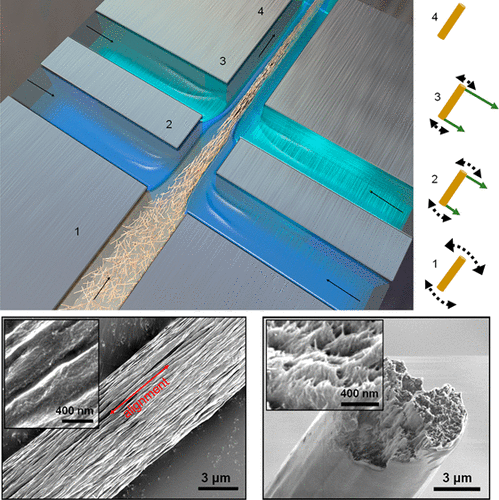
The scientists started with commercially available cellulose nanofibres that are just 2 to 5 nanometres in diameter and up to 700 nanometres long. A nanometre (nm) is a millionth of a millimetre. The nanofibres were suspended in water and fed into a small channel, just one millimetre wide and milled in steel. Through two pairs of perpendicular inflows additional deionized water and water with a low pH-value entered the channel from the sides, squeezing the stream of nanofibres together and accelerating it.
This process, called hydrodynamic focussing, helped to align the nanofibres in the right direction as well as their self-organisation into a well-packed macroscopic thread. No glue or any other component is needed, the nanofibres assemble into a tight thread held together by supramolecular forces between the nanofibres, for example electrostatic and Van der Waals forces.
With the bright X-rays from PETRA III the scientists could follow and optimise the process. “The X-rays allow us to analyse the detailed structure of the thread as it forms as well as the material structure and hierarchical order in the super strong fibres,” explains co-author Stephan Roth from DESY, head of the Micro- and Nanofocus X-ray Scattering Beamline P03 where the threads were spun. “We made threads up to 15 micrometres thick and several metres in length.”
Measurements showed a tensile stiffness of 86 gigapascals (GPa) for the material and a tensile strength of 1.57 GPa. “The bio-based nanocellulose fibres fabricated here are 8 times stiffer and have strengths higher than natural dragline spider silk fibres,” says Söderberg. “If you are looking for a bio-based material, there is nothing quite like it. And it is also stronger than steel and any other metal or alloy as well as glass fibres and most other synthetic materials.” The artificial cellulose fibres can be woven into a fabric to create materials for various applications. The researchers estimate that the production costs of the new material can compete with those of strong synthetic fabrics. “The new material can in principle be used to create bio-degradable components,” adds Roth.
The study describes a new method that mimics nature’s ability to accumulate cellulose nanofibres into almost perfect macroscale arrangements, like in wood. It opens the way for developing nanofibre material that can be used for larger structures while retaining the nanofibres’ tensile strength and ability to withstand mechanical load. “We can now transform the super performance from the nanoscale to the macroscale,” Söderberg underlines. “This discovery is made possible by understanding and controlling the key fundamental parameters essential for perfect nanostructuring, such as particle size, interactions, alignment, diffusion, network formation and assembly.” The process can also be used to control nanoscale assembly of carbon tubes and other nano-sized fibres.
(There are some terminology and spelling issues, which are described at the end of this post.)
Let’s get back to a material that rivals spider silk and steel for strength (for some reason that reminded me of an old carnival game where you’d test your strength by swinging a mallet down on a ‘teeter-totter-like’ board and sending a metal piece up a post to make a bell ring). From a May 16, 2018 DESY press release (also on EurekAlert), which originated the news item,
The ultrastrong material is made of cellulose nanofibres (CNF), the essential building blocks of wood and other plant life. Using a novel production method, the researchers have successfully transferred the unique mechanical properties of these nanofibres to a macroscopic, lightweight material that could be used as an eco-friendly alternative for plastic in airplanes, cars, furniture and other products. “Our new material even has potential for biomedicine since cellulose is not rejected by your body”, explains Söderberg.
The scientists started with commercially available cellulose nanofibres that are just 2 to 5 nanometres in diameter and up to 700 nanometres long. A nanometre (nm) is a millionth of a millimetre. The nanofibres were suspended in water and fed into a small channel, just one millimetre wide and milled in steel. Through two pairs of perpendicular inflows additional deionized water and water with a low pH-value entered the channel from the sides, squeezing the stream of nanofibres together and accelerating it.
This process, called hydrodynamic focussing, helped to align the nanofibres in the right direction as well as their self-organisation into a well-packed macroscopic thread. No glue or any other component is needed, the nanofibres assemble into a tight thread held together by supramolecular forces between the nanofibres, for example electrostatic and Van der Waals forces.
With the bright X-rays from PETRA III the scientists could follow and optimise the process. “The X-rays allow us to analyse the detailed structure of the thread as it forms as well as the material structure and hierarchical order in the super strong fibres,” explains co-author Stephan Roth from DESY, head of the Micro- and Nanofocus X-ray Scattering Beamline P03 where the threads were spun. “We made threads up to 15 micrometres thick and several metres in length.”
Measurements showed a tensile stiffness of 86 gigapascals (GPa) for the material and a tensile strength of 1.57 GPa. “The bio-based nanocellulose fibres fabricated here are 8 times stiffer and have strengths higher than natural dragline spider silk fibres,” says Söderberg. “If you are looking for a bio-based material, there is nothing quite like it. And it is also stronger than steel and any other metal or alloy as well as glass fibres and most other synthetic materials.” The artificial cellulose fibres can be woven into a fabric to create materials for various applications. The researchers estimate that the production costs of the new material can compete with those of strong synthetic fabrics. “The new material can in principle be used to create bio-degradable components,” adds Roth.
The study describes a new method that mimics nature’s ability to accumulate cellulose nanofibres into almost perfect macroscale arrangements, like in wood. It opens the way for developing nanofibre material that can be used for larger structures while retaining the nanofibres’ tensile strength and ability to withstand mechanical load. “We can now transform the super performance from the nanoscale to the macroscale,” Söderberg underlines. “This discovery is made possible by understanding and controlling the key fundamental parameters essential for perfect nanostructuring, such as particle size, interactions, alignment, diffusion, network formation and assembly.” The process can also be used to control nanoscale assembly of carbon tubes and other nano-sized fibres.
Here’s a link to and a citation for the paper,
Multiscale Control of Nanocellulose Assembly: Transferring Remarkable Nanoscale Fibril Mechanics to Macroscale Fibers by Nitesh Mittal, Farhan Ansari, Krishne Gowda V, Christophe Brouzet, Pan Chen, Per Tomas Larsson, Stephan V. Roth, Fredrik Lundell, Lars Wågberg, Nicholas A. Kotov, and L. Daniel Söderberg. ACS Nano, Article ASAP DOI: 10.1021/acsnano.8b01084 Publication Date (Web): May 9, 2018
Copyright © 2018 American Chemical Society
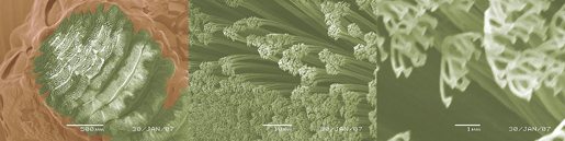
This paper is open access and accompanied by this image illustrating the work,
Courtesy: American Chemical Society and the researchers [Note: The bottom two images of cellulose nanofibres, which are constittuents of an artificial cellulose fibre, appear to be from a scanning tunneling microsscope. Credit: Nitesh Mittal, KTH Stockholm
This news has excited interest at General Electric (GE) (its
Wikipedia entry), which has highlighted the work in a May 25, 2018 posting (
The 5 Coolest Things On Earth This Week) by Tomas Kellner on the GE Reports blog.
Terminology and spelling
I’ll start with spelling since that’s the easier of the two. In some parts of the world it’s spelled ‘fibres’ and in other parts of the world it’s spelled ‘fibers’. When I write the text in my post, it tends to reflect the spelling used in the news/press releases. In other words, I swing in whichever direction the wind is blowing.
For diehards only
As i understand the terminology situation, nanocellulose and cellulose nanomaterials are interchangeable generic terms. Further, cellulose nanofibres (CNF) seems to be another generic term and it encompasses both cellulose nanocrystals (CNC) and cellulose nanofibrils (CNF). Yes, there appear to be two CNFs. Making matters more interesting is the fact that cellulose nanocrystals were originally christened nanocrystalline cellulose (NCC). For anyone who follows the science and technology scene, it becomes obvious that competing terminologies are the order of the day. Eventually the dust settles and naming conventions are resolved. More or less.
Ordinarily I would reference the Nanocellulose Wikipedia entry in my attempts to clarify the issues but it seems that the writers for the entry have not caught up to the current naming convention for cellulose nanocrystals, still referring to the material as nanocrystalline cellulose. This means, I can’t trust the rest of the entry, which has only one CNF (cellulose nanofibres).
I have paid more attention to the NCC/CNC situation and am not as familiar with the CNF situation. Using, NCC/CNC as an example of a terminology issue, I believe it was first developed in Canada and it was Canadian researchers who were pushing their NCC terminology while the international community pushed back with CNC.
In the end, NCC became a brand name, which was trademarked by CelluForce, a Canadian company in the CNC market. From the CelluForce Products page on Cellulose Nanocrystals,
…
CNC are not all made equal. The CNC produced by CelluForce is called CelluForce NCCTM and has specific properties and are especially easy to disperse. CelluForce NCCTM is the base material that CelluForce uses in all its products. This base material can be modified and tailored to suit the specific needs in various applications.
These, days CNC is almost universally used but NCC (not as a trademark) is a term still employed on occasion (and, oddly, the researchers are not necessarily Canadian).
Should anyone have better information about terminology issues, please feel free to comment.