Tag Archives: white graphene

Sticky tape, hackers, and quantum communications

I always appreciate a low technology solution to a problem. In this case, it’s a piece of sticky tape which halts compute hackers in their tracks. Here’s more from an August 30, 2021 University of Technology Sydney press release (also on EurekAlert but published August 26, 2021), Note: Links have been removed,

Researchers from the University of Technology Sydney (UTS) and TMOS, an Australian Research Council Centre of Excellence [specifically, the Australian Research Council Centre of Excellence for Transformative Meta-Optical Systems (TMOS)], have taken the fight to online hackers with a giant leap towards realizing affordable, accessible quantum communications, a technology that would effectively prevent the decryption of online activity. Everything from private social media messaging to banking could become more secure due to new technology created with a humble piece of adhesive tape.

Quantum communication is still in its early development and is currently feasible only in very limited fields due to the costs associated with fabricating the required devices. The TMOS researches have developed new technology that integrates quantum sources and waveguides on chip in a manner that is both affordable and scalable, paving the way for future everyday use.

The development of fully functional quantum communication technologies has previously been hampered by the lack of reliable quantum light sources that can encode and transmit the information.

In a paper published today in ACS Photonics, the team describes a new platform to generate these quantum emitters based on hexagonal boron nitride, also known as white graphene. Where current quantum emitters are created using complex methods in expensive clean rooms, these new quantum emitters can be created using $20 worth of white graphene pressed on to a piece of adhesive tape.

These 2D materials can be pressed onto a sticky surface such as the [sic] adhesive tape [emphasis mine] and exfoliated, which is essentially peeling off the top layer to create a flex. Multiple layers of this flex can then be assembled in a Lego-like style, offering a new bottom up approach as a substitute for 3D systems.

TMOS Chief Investigator Igor Aharonovich said: “2D materials, like hexagonal boron nitride, are emerging materials for integrated quantum photonics, and are poised to impact the way we design and engineer future optical components for secured communication.”

In addition to this evolution in photon sources, the team has developed a high efficiency on-chip waveguide, a vital component for on-chip optical processing.

Lead author Chi Li said: “Low signal levels have been a significant barrier preventing quantum communications from evolving into practical, workable models. We hope that with this new development, quantum comms will become an everyday technology that improves people’s lives in new and exciting ways.”

Here’s a link to and a citation for the paper,

Integration of hBN Quantum Emitters in Monolithically Fabricated Waveguides by Chi Li, Johannes E. Fröch, Milad Nonahal, Thinh N. Tran, Milos Toth, Sejeong Kim, and Igor Aharonovich. ACS Photonics 2021, XXXX, XXX, XXX-XXX DOI: https://doi.org/10.1021/acsphotonics.1c00890 Publication Date:August 20, 2021 © 2021 American Chemical Society

This paper is behind a paywall.

Sticky or adhesive tape is part of graphene lore and seems to exert a great fascination for scientists as I note in my June 12, 2018 posting.

‘Lilliputian’ skyscraper: white graphene for hydrogen storage

This story comes from Rice University (Texas, US). From a March 12, 2018 news item on Nanowerk,

Rice University engineers have zeroed in on the optimal architecture for storing hydrogen in “white graphene” nanomaterials — a design like a Lilliputian skyscraper with “floors” of boron nitride sitting one atop another and held precisely 5.2 angstroms apart by boron nitride pillars.
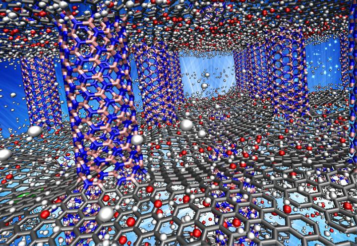
Caption Thousands of hours of calculations on Rice University’s two fastest supercomputers found that the optimal architecture for packing hydrogen into “white graphene” involves making skyscraper-like frameworks of vertical columns and one-dimensional floors that are about 5.2 angstroms apart. In this illustration, hydrogen molecules (white) sit between sheet-like floors of graphene (gray) that are supported by boron-nitride pillars (pink and blue). Researchers found that identical structures made wholly of boron-nitride had unprecedented capacity for storing readily available hydrogen. Credit Lei Tao/Rice University

A March 12, 2018 Rice University news release (also on EurekAlert), which originated the news item, goes into extensive detail about the work,

“The motivation is to create an efficient material that can take up and hold a lot of hydrogen — both by volume and weight — and that can quickly and easily release that hydrogen when it’s needed,”  [emphasis mine] said the study’s lead author, Rouzbeh Shahsavari, assistant professor of civil and environmental engineering at Rice.

Hydrogen is the lightest and most abundant element in the universe, and its energy-to-mass ratio — the amount of available energy per pound of raw material, for example — far exceeds that of fossil fuels. It’s also the cleanest way to generate electricity: The only byproduct is water. A 2017 report by market analysts at BCC Research found that global demand for hydrogen storage materials and technologies will likely reach $5.4 billion annually by 2021.

Hydrogen’s primary drawbacks relate to portability, storage and safety. While large volumes can be stored under high pressure in underground salt domes and specially designed tanks, small-scale portable tanks — the equivalent of an automobile gas tank — have so far eluded engineers.

Following months of calculations on two of Rice’s fastest supercomputers, Shahsavari and Rice graduate student Shuo Zhao found the optimal architecture for storing hydrogen in boron nitride. One form of the material, hexagonal boron nitride (hBN), consists of atom-thick sheets of boron and nitrogen and is sometimes called white graphene because the atoms are spaced exactly like carbon atoms in flat sheets of graphene.

Previous work in Shahsavari’s Multiscale Materials Lab found that hybrid materials of graphene and boron nitride could hold enough hydrogen to meet the Department of Energy’s storage targets for light-duty fuel cell vehicles.

“The choice of material is important,” he said. “Boron nitride has been shown to be better in terms of hydrogen absorption than pure graphene, carbon nanotubes or hybrids of graphene and boron nitride.

“But the spacing and arrangement of hBN sheets and pillars is also critical,” he said. “So we decided to perform an exhaustive search of all the possible geometries of hBN to see which worked best. We also expanded the calculations to include various temperatures, pressures and dopants, trace elements that can be added to the boron nitride to enhance its hydrogen storage capacity.”

Zhao and Shahsavari set up numerous “ab initio” tests, computer simulations that used first principles of physics. Shahsavari said the approach was computationally intense but worth the extra effort because it offered the most precision.

“We conducted nearly 4,000 ab initio calculations to try and find that sweet spot where the material and geometry go hand in hand and really work together to optimize hydrogen storage,” he said.

Unlike materials that store hydrogen through chemical bonding, Shahsavari said boron nitride is a sorbent that holds hydrogen through physical bonds, which are weaker than chemical bonds. That’s an advantage when it comes to getting hydrogen out of storage because sorbent materials tend to discharge more easily than their chemical cousins, Shahsavari said.

He said the choice of boron nitride sheets or tubes and the corresponding spacing between them in the superstructure were the key to maximizing capacity.

“Without pillars, the sheets sit naturally one atop the other about 3 angstroms apart, and very few hydrogen atoms can penetrate that space,” he said. “When the distance grew to 6 angstroms or more, the capacity also fell off. At 5.2 angstroms, there is a cooperative attraction from both the ceiling and floor, and the hydrogen tends to clump in the middle. Conversely, models made of purely BN tubes — not sheets — had less storage capacity.”

Shahsavari said models showed that the pure hBN tube-sheet structures could hold 8 weight percent of hydrogen. (Weight percent is a measure of concentration, similar to parts per million.) Physical experiments are needed to verify that capacity, but that the DOE’s ultimate target is 7.5 weight percent, and Shahsavari’s models suggests even more hydrogen can be stored in his structure if trace amounts of lithium are added to the hBN.

Finally, Shahsavari said, irregularities in the flat, floor-like sheets of the structure could also prove useful for engineers.

“Wrinkles form naturally in the sheets of pillared boron nitride because of the nature of the junctions between the columns and floors,” he said. “In fact, this could also be advantageous because the wrinkles can provide toughness. If the material is placed under load or impact, that buckled shape can unbuckle easily without breaking. This could add to the material’s safety, which is a big concern in hydrogen storage devices.

“Furthermore, the high thermal conductivity and flexibility of BN may provide additional opportunities to control the adsorption and release kinetics on-demand,” Shahsavari said. “For example, it may be possible to control release kinetics by applying an external voltage, heat or an electric field.”

I may be wrong but this “The motivation is to create an efficient material that can take up and hold a lot of hydrogen — both by volume and weight — and that can quickly and easily release that hydrogen when it’s needed, …”  sounds like a supercapacitor. One other comment, this research appears to be ‘in silico’, i.e., all the testing has been done as computer simulations and the proposed materials themselves have yet to be tested.

Here’s a link to and a citation for the paper,

Merger of Energetic Affinity and Optimal Geometry Provides New Class of Boron Nitride Based Sorbents with Unprecedented Hydrogen Storage Capacity by Rouzbeh Shahsavari and Shuo Zhao. Small Vol. 14 Issue 10 DOI: 10.1002/smll.201702863 Version of Record online: 8 MAR 2018

© 2018 WILEY-VCH Verlag GmbH & Co. KGaA, Weinheim

This paper is behind a paywall.

Three teams observe graphene butterflies

It took me a few minutes to find the butterflies (visual pattern recognition is not one of my strengths) but here they are,

Caption: Graphene, combined with white graphene, forms stunning 'butterfly' images. Credit: The University of Manchester

Caption: Graphene, combined with white graphene, forms stunning ‘butterfly’ images.
Credit: The University of Manchester

The May 15, 2013 University of Manchester news release (on EurekAlert and on the University of Manchester news site) describes how the ‘butterflies’ are formed,

Writing in Nature, a large international team led Dr Roman Gorbachev from The University of Manchester shows that, when graphene placed on top of insulating boron nitride, or ‘white graphene’, the electronic properties of graphene change dramatically revealing a pattern resembling a butterfly.

The pattern is referred to as the elusive Hofstadter butterfly that has been known in theory for many decades but never before observed in experiments.

More of the science needs to be explained before moving on with the ‘butterflies’ (from the news release),

One of the most remarkable properties of graphene is its high conductivity – thousands of times higher than copper. This is due to a very special pattern created by electrons that carry electricity in graphene. The carriers are called Dirac fermions and mimic massless relativistic particles called neutrinos, studies of which usually require huge facilities such as at CERN. The possibility to address similar physics in a desk-top experiment is one of the most renowned features of graphene.

Now the Manchester scientists have found a way to create multiple clones of Dirac fermions. Graphene is placed on top of boron nitride so that graphene’s electrons can ‘feel’ individual boron and nitrogen atoms. Moving along this atomic ‘washboard’, electrons rearrange themselves once again producing multiple copies of the original Dirac fermions.

Here’s where the butterflies appear (from the news release),

The researchers can create even more clones by applying a magnetic field. The clones produce an intricate pattern; the Hofstadter butterfly. It was first predicted by mathematician Douglas Hofstadter in 1976 and, despite many dedicated experimental efforts, no more than a blurred glimpse was reported before.

In addition to the described fundamental interest, the Manchester study proves that it is possible to modify properties of atomically-thin materials by placing them on top of each other. This can be useful, for example, for graphene applications such as ultra-fast photodetectors and transistors, providing a way to tweak its incredible properties.

Coincidentally, another team has also observed the Hofstadter butterfly on a graphene substrate. From the May 16, 2013 news item on Azonano,

Two research teams at the National High Magnetic Field Laboratory (MagLab) broke through a nearly 40-year barrier recently when they observed a never-before-seen energy pattern.

“The observation of the ‘Hofstadter butterfly’ marks a real landmark in condensed matter physics and high magnetic field research,” said Greg Boebinger, director of the MagLab. “It opens a new experimental direction in materials research.”

This groundbreaking research demanded the ability to measure samples of materials at very low temperatures and very high magnetic fields, up to 35 tesla. Both of those conditions are available at the MagLab, making it an international destination for scientific exploration.

The unique periodic structure used to observe the butterfly pattern was composed of boron nitride (BN) and graphene.

The May 15, 2013 Florida State University news release by Kristin Roberts, which originated the news item, describes the two teams using the MagLab facilities for their ‘butterfly’ observations,

One research team was led by Columbia University’s Philip Kim and included researchers from City University of New York, the University of Central Florida, Tohoku University and the National Institute for Materials Science in Japan. The team’s work will be published today in the Advanced Online Publication of the journal Nature. Similar results were discovered at the MagLab by a group led by Pablo Jarillo-Herrero and Raymond Ashoori at MIT, as well as scientists from Tohoku University and the National Institute for Materials Science in Japan. Their work is expected to be published soon.

For those who just can’t get enough graphene butterflies here are citations for and links to both recently published papers (the Jarillo-Herrero/Ashoori team will be publishing their work soon).

Cloning of Dirac fermions in graphene superlattices by L. A. Ponomarenko, R. V. Gorbachev, G. L. Yu,D. C. Elias, R. Jalil, A. A. Patel, A. Mishchenko, A. S. Mayorov, C. R. Woods, J. R. Wallbank, M. Mucha-Kruczynski, B. A. Piot, M. Potemski, I. V. Grigorieva, K. S. Novoselov, F. Guinea, V. I. Fal’ko & A. K. Geim. Nature doi:10.1038/nature12187 Published online   

and,

Hofstadter’s butterfly and the fractal quantum Hall effect in moiré superlattices by C. R. Dean, L. Wang, P. Maher, C. Forsythe, F. Ghahari, Y. Gao, J. Katoch, M. Ishigami, P. Moon, M. Koshino, T. Taniguchi, K. Watanabe, K. L. Shepard, J. Hone & P. Kim. Nature (2013) doi:10.1038/nature12186 Published online 15 May 2013

Both papers are behind paywalls.