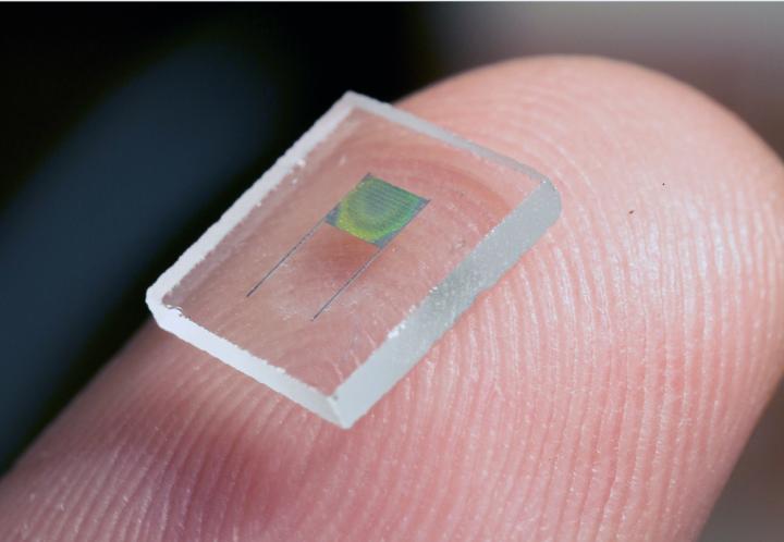
Caption: This is an image of the holographically patterned microbattery.
Credit: University of Illinois
Hard to believe that’s a battery but the researchers at the University of Illinois assure us this is so according to a May 11, 2015 news item on Nanowerk,
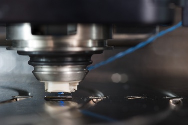
By combining 3D holographic lithography and 2D photolithography, researchers from the University of Illinois at Urbana-Champaign have demonstrated a high-performance 3D microbattery suitable for large-scale on-chip integration with microelectronic devices.
“This 3D microbattery has exceptional performance and scalability, and we think it will be of importance for many applications,” explained Paul Braun, a professor of materials science and engineering at Illinois. “Micro-scale devices typically utilize power supplied off-chip because of difficulties in miniaturizing energy storage technologies. A miniaturized high-energy and high-power on-chip battery would be highly desirable for applications including autonomous microscale actuators, distributed wireless sensors and transmitters, monitors, and portable and implantable medical devices.”
A May 11, 2015 University of Illinois news release on EurkeAlert, which originated the news item, provides some insight into and detail about the research,
“Due to the complexity of 3D electrodes, it is generally difficult to realize such batteries, let alone the possibility of on-chip integration and scaling. In this project, we developed an effective method to make high-performance 3D lithium-ion microbatteries using processes that are highly compatible with the fabrication of microelectronics,” stated Hailong Ning, a graduate student in the Department of Materials Science and Engineering and first author of the article, “Holographic Patterning of High Performance on-chip 3D Lithium-ion Microbatteries,” appearing in Proceedings of the National Academy of Sciences.
“We utilized 3D holographic lithography to define the interior structure of electrodes and 2D photolithography to create the desired electrode shape.” Ning added. “This work merges important concepts in fabrication, characterization, and modeling, showing that the energy and power of the microbattery are strongly related to the structural parameters of the electrodes such as size, shape, surface area, porosity, and tortuosity. A significant strength of this new method is that these parameters can be easily controlled during lithography steps, which offers unique flexibility for designing next-generation on-chip energy storage devices.”
Enabled by a 3D holographic patterning technique–where multiple optical beams interfere inside the photoresist creating a desirable 3D structure–the battery possesses well-defined, periodically structured porous electrodes, that facilitates the fast transports of electrons and ions inside the battery, offering supercapacitor-like power.
“Although accurate control on the interfering optical beams is required to construct 3D holographic lithography, recent advances have significantly simplified the required optics, enabling creation of structures via a single incident beam and standard photoresist processing. This makes it highly scalable and compatible with microfabrication,” stated John Rogers, a professor of materials science and engineering, who has worked with Braun and his team to develop the technology.
“Micro-engineered battery architectures, combined with high energy material such as tin, offer exciting new battery features including high energy capacity and good cycle lives, which provide the ability to power practical devices,” stated William King, a professor of mechanical science and engineering, who is a co-author of this work.
Here’s a link to and a citation for the paper,
Holographic patterning of high-performance on-chip 3D lithium-ion microbatteries by Hailong Ning, James H. Pikul, Runyu Zhang, Xuejiao Li, Sheng Xu, Junjie Wang, John A. Rogers, William P. King, and Paul V. Braun. PNAS doi: 10.1073/pnas.1423889112
This paper is behind a paywall.