This is quite the week for see-through medical devices based on graphene. A second team has developed a transparent sensor which could allow scientists to make observations of brain activity that are now impossible, according to an Oct. 20, 2014 University of Wisconsin-Madison news release (also on EurekAlert),
Neural researchers study, monitor or stimulate the brain using imaging techniques in conjunction with implantable sensors that allow them to continuously capture and associate fleeting brain signals with the brain activity they can see.
However, it’s difficult to see brain activity when there are sensors blocking the view.
“One of the holy grails of neural implant technology is that we’d really like to have an implant device that doesn’t interfere with any of the traditional imaging diagnostics,” says Justin Williams, the Vilas Distinguished Achievement Professor of biomedical engineering and neurological surgery at UW-Madison. “A traditional implant looks like a square of dots, and you can’t see anything under it. We wanted to make a transparent electronic device.”
The researchers chose graphene, a material gaining wider use in everything from solar cells to electronics, because of its versatility and biocompatibility. And in fact, they can make their sensors incredibly flexible and transparent because the electronic circuit elements are only 4 atoms thick—an astounding thinness made possible by graphene’s excellent conductive properties. “It’s got to be very thin and robust to survive in the body,” says Zhenqiang (Jack) Ma, the Lynn H. Matthias Professor and Vilas Distinguished Achievement Professor of electrical and computer engineering at UW-Madison. “It is soft and flexible, and a good tradeoff between transparency, strength and conductivity.”
Drawing on his expertise in developing revolutionary flexible electronics, he, Williams and their students designed and fabricated the micro-electrode arrays, which—unlike existing devices—work in tandem with a range of imaging technologies. “Other implantable micro-devices might be transparent at one wavelength, but not at others, or they lose their properties,” says Ma. “Our devices are transparent across a large spectrum—all the way from ultraviolet to deep infrared.”
The transparent sensors could be a boon to neuromodulation therapies, which physicians increasingly are using to control symptoms, restore function, and relieve pain in patients with diseases or disorders such as hypertension, epilepsy, Parkinson’s disease, or others, says Kip Ludwig, a program director for the National Institutes of Health neural engineering research efforts. “Despite remarkable improvements seen in neuromodulation clinical trials for such diseases, our understanding of how these therapies work—and therefore our ability to improve existing or identify new therapies—is rudimentary.”
Currently, he says, researchers are limited in their ability to directly observe how the body generates electrical signals, as well as how it reacts to externally generated electrical signals. “Clear electrodes in combination with recent technological advances in optogenetics and optical voltage probes will enable researchers to isolate those biological mechanisms. This fundamental knowledge could be catalytic in dramatically improving existing neuromodulation therapies and identifying new therapies.”
The advance aligns with bold goals set forth in President Barack Obama’s BRAIN (Brain Research through Advancing Innovative Neurotechnologies) Initiative. Obama announced the initiative in April 2013 as an effort to spur innovations that can revolutionize understanding of the brain and unlock ways to prevent, treat or cure such disorders as Alzheimer’s and Parkinson’s disease, post-traumatic stress disorder, epilepsy, traumatic brain injury, and others.
The UW-Madison researchers developed the technology with funding from the Reliable Neural-Interface Technology program at the Defense Advanced Research Projects Agency.
While the researchers centered their efforts around neural research, they already have started to explore other medical device applications. For example, working with researchers at the University of Illinois-Chicago, they prototyped a contact lens instrumented with dozens of invisible sensors to detect injury to the retina; the UIC team is exploring applications such as early diagnosis of glaucoma.
Here’s an image of the see-through medical implant,
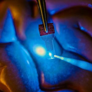
Caption: A blue light shines through a clear implantable medical sensor onto a brain model. See-through sensors, which have been developed by a team of University of Wisconsin Madison engineers, should help neural researchers better view brain activity.
Credit: Justin Williams research group
Here’s a link to and a citation for the paper,
Graphene-based carbon-layered electrode array technology for neural imaging and optogenetic applications by Dong-Wook Park, Amelia A. Schendel, Solomon Mikael, Sarah K. Brodnick, Thomas J. Richner, Jared P. Ness, Mohammed R. Hayat, Farid Atry, Seth T. Frye, Ramin Pashaie, Sanitta Thongpang, Zhenqiang Ma, & Justin C. Williams. Nature Communications 5, Article number: 5258 doi:10.1038/ncomms6258 Published
20 October 2014
This is an open access paper.
DARPA (US Defense Advanced Research Projects Agency), which funds this work at the University of Wisconsin-Madison, has also provided an Oct. 20, 2014 news release (also published an an Oct. 27, 2014 news item on Nanowerk) describing this research from the military perspective, which may not be what you might expect. First, here’s a description of the DARPA funding programme underwriting this research, from DARPA’s Reliable Neural-Interface Technology (RE-NET) webpage,
Advancing technology for military uniforms, body armor and equipment have saved countless lives of our servicemembers injured on the battlefield. Unfortunately, many of those survivors are seriously and permanently wounded, with unprecedented rates of limb loss and traumatic brain injury among our returning soldiers. This crisis has motivated great interest in the science of and technology for restoring sensorimotor functions lost to amputation and injury of the central nervous system. For a decade now, DARPA has been leading efforts aimed at ‘revolutionizing’ the state-of-the-art in prosthetic limbs, recently debuting 2 advanced mechatronic limbs for the upper extremity. These new devices are truly anthropomorphic and capable of performing dexterous manipulation functions that finally begin to approach the capabilities of natural limbs. However, in the absence of a high bandwidth, intuitive interface for the user, these limbs will never achieve their full potential in improving the quality of life for the wounded soldiers that could benefit from this advanced technology.
DARPA created the Reliable Neural-Interface Technology (RE-NET) program in 2010 to directly address the need for high performance neural interfaces to control dexterous functions made possible with advanced prosthetic limbs. Specifically, RE-NET seeks to develop the technologies needed to reliably extract information from the nervous system, and to do so at a scale and rate necessary to control many degree-of-freedom (DOF) machines, such as high-performance prosthetic limbs. Prior to the DARPA RE-NET program, all existing methods to extract neural control signals were inadequate for amputees to control high-performance prostheses, either because the level of extracted information was too low or the functional lifetime was too short. However, recent technological advances create new opportunities to solve both of these neural-interface problems. For example, it is now feasible to develop high-resolution peripheral neuromuscular interfaces that increase the amount of information obtained from the peripheral nervous system. Furthermore, advances in cortical microelectrode technologies are extending the durability of neural signals obtained from the brain, making it possible to create brain-controlled prosthetics that remain useful over the full lifetime of the patient.