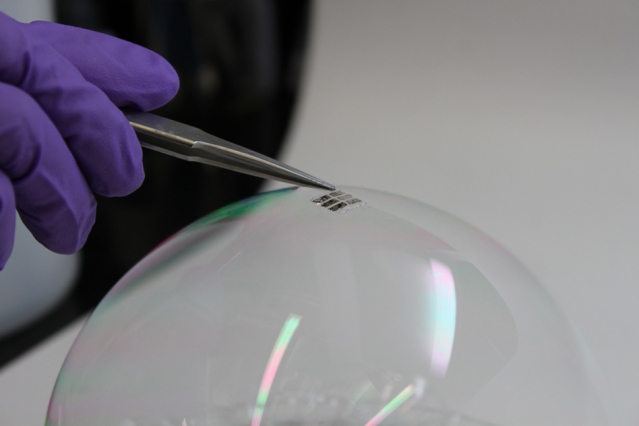
The MIT team has achieved the thinnest and lightest complete solar cells ever made, they say. To demonstrate just how thin and lightweight the cells are, the researchers draped a working cell on top of a soap bubble, without popping the bubble. Photo: Joel Jean and Anna Osherov
That’s quite a compelling image and it comes to us courtesy of researchers at MIT (Massachusetts Institute of Technology). From a Feb. 25, 2016 MIT news release (also on EurekAlert),
Imagine solar cells so thin, flexible, and lightweight that they could be placed on almost any material or surface, including your hat, shirt, or smartphone, or even on a sheet of paper or a helium balloon.
Researchers at MIT have now demonstrated just such a technology: the thinnest, lightest solar cells ever produced. Though it may take years to develop into a commercial product, the laboratory proof-of-concept shows a new approach to making solar cells that could help power the next generation of portable electronic devices.
…
Bulović [Vladimir Bulović ], MIT’s associate dean for innovation and the Fariborz Maseeh (1990) Professor of Emerging Technology, says the key to the new approach is to make the solar cell, the substrate that supports it, and a protective overcoating to shield it from the environment, all in one process. The substrate is made in place and never needs to be handled, cleaned, or removed from the vacuum during fabrication, thus minimizing exposure to dust or other contaminants that could degrade the cell’s performance.
“The innovative step is the realization that you can grow the substrate at the same time as you grow the device,” Bulović says.
In this initial proof-of-concept experiment, the team used a common flexible polymer called parylene as both the substrate and the overcoating, and an organic material called DBP as the primary light-absorbing layer. Parylene is a commercially available plastic coating used widely to protect implanted biomedical devices and printed circuit boards from environmental damage. The entire process takes place in a vacuum chamber at room temperature and without the use of any solvents, unlike conventional solar-cell manufacturing, which requires high temperatures and harsh chemicals. In this case, both the substrate and the solar cell are “grown” using established vapor deposition techniques.
One process, many materials
The team emphasizes that these particular choices of materials were just examples, and that it is the in-line substrate manufacturing process that is the key innovation. Different materials could be used for the substrate and encapsulation layers, and different types of thin-film solar cell materials, including quantum dots or perovskites, could be substituted for the organic layers used in initial tests.
But already, the team has achieved the thinnest and lightest complete solar cells ever made, they say. To demonstrate just how thin and lightweight the cells are, the researchers draped a working cell on top of a soap bubble, without popping the bubble. The researchers acknowledge that this cell may be too thin to be practical — “If you breathe too hard, you might blow it away,” says Jean [Joel Jean, doctoral student] — but parylene films of thicknesses of up to 80 microns can be deposited easily using commercial equipment, without losing the other benefits of in-line substrate formation.
A flexible parylene film, similar to kitchen cling-wrap but only one-tenth as thick, is first deposited on a sturdier carrier material – in this case, glass. Figuring out how to cleanly separate the thin material from the glass was a key challenge, explains Wang [Annie Wang, research scientist], who has spent many years working with parylene.
The researchers lift the entire parylene/solar cell/parylene stack off the carrier after the fabrication process is complete, using a frame made of flexible film. The final ultra-thin, flexible solar cells, including substrate and overcoating, are just one-fiftieth of the thickness of a human hair and one-thousandth of the thickness of equivalent cells on glass substrates — about two micrometers thick — yet they convert sunlight into electricity just as efficiently as their glass-based counterparts.
No miracles needed
“We put our carrier in a vacuum system, then we deposit everything else on top of it, and then peel the whole thing off,” explains Wang. Bulović says that like most new inventions, it all sounds very simple — once it’s been done. But actually developing the techniques to make the process work required years of effort.
While they used a glass carrier for their solar cells, Jean says “it could be something else. You could use almost any material,” since the processing takes place under such benign conditions. The substrate and solar cell could be deposited directly on fabric or paper, for example.
While the solar cell in this demonstration device is not especially efficient, because of its low weight, its power-to-weight ratio is among the highest ever achieved. That’s important for applications where weight is important, such as on spacecraft or on high-altitude helium balloons used for research. Whereas a typical silicon-based solar module, whose weight is dominated by a glass cover, may produce about 15 watts of power per kilogram of weight, the new cells have already demonstrated an output of 6 watts per gram — about 400 times higher.
“It could be so light that you don’t even know it’s there, on your shirt or on your notebook,” Bulović says. “These cells could simply be an add-on to existing structures.”
Still, this is early, laboratory-scale work, and developing it into a manufacturable product will take time, the team says. Yet while commercial success in the short term may be uncertain, this work could open up new applications for solar power in the long term. “We have a proof-of-concept that works,” Bulović says. The next question is, “How many miracles does it take to make it scalable? We think it’s a lot of hard work ahead, but likely no miracles needed.”
Here’s a link to and a citation for the paper,
In situ vapor-deposited parylene substrates for ultra-thin, lightweight organic solar cells by Joel Jean, Annie Wang, Vladimir Bulović. Organic Electronics Volume 31, April 2016, Pages 120–126 doi:10.1016/j.orgel.2016.01.022
This paper is behind a paywall.
