Apparently, the Morpho butterfly (or blue morpho butterfly) could inspire more balanced lighting, from an October 12, 2023 news item on phys.org,
As you watch Morpho butterflies wobble in flight, shimmering in vivid blue color, you’re witnessing an uncommon form of structural color that researchers are only beginning to use in lighting technologies such as optical diffusers. Furthermore, imparting a self-cleaning capability to such diffusers would minimize soiling and staining and maximize practical utility.
Now, in a study recently published in Advanced Optical Materials, researchers at Osaka University have developed a water-repelling nanostructured light diffuser that surpasses the functionality of other common diffusers. This work might help solve common lighting dilemmas in modern technologies.
…
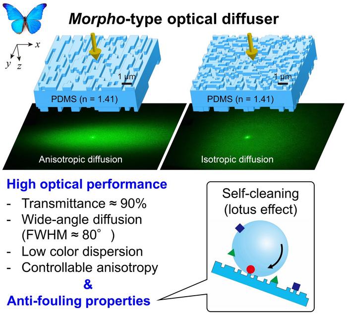
Caption: Design and diffused light for the anisotropic (left) and isotropic (right) Morpho-type diffusers. It has high optical functionalities and anti-fouling properties, which until now have not been realized in one device. Credit: K.Yamashita, A.Saito
Standard lighting can eventually become tiring because it’s unevenly illuminating. Thus, many display technologies use optical diffusers to make the light output more uniform. However, conventional optical diffusers reduce the light output, don’t work well for all emitted colors, or require special effort to clean. Morpho butterflies are an inspiration for improved optical diffusers. Their randomly arranged multilayer architecture enables structural color: in this case, selective reflection of blue light over a ≥±40° angle from the direction of illumination. The goal of the present work is to use this inspiration from nature to design a simplified optical diffuser that has both high transmittance and wide angular spread, works for a range of colors without dispersion, cleans by a simple water rinse, and can be shaped with standard nanofabrication tools.
“We create two-dimensional nanopatterns—in common transparent polydimethylsiloxane elastomer—of binary height yet random width, and the two surfaces have different structural scales,” explains Kazuma Yamashita, lead author of the study. “Thus, we report an effective optical diffuser for short- and long-wavelength light.”
The researchers tailored the patterns of the diffuser surfaces to optimize the performance for blue and red light, and their self-cleaning properties. The experimentally measured light transmittance was >93% over the entire visible light spectrum, and the light diffusion was substantial and could be controlled into anisotropic shape: 78° in the x-direction and 16° in the y-direction (similar to values calculated by simulations). Furthermore, the surfaces both strongly repelled water in contact angle and self-cleaning experiments.
“Applying protective cover glass layers on either side of the optical diffuser largely maintains the optical properties, yet protects against scratching,” says Akira Saito, senior author. “The glass minimizes the need for careful handling, and indicates our technology’s utility to daylight-harvesting windows.”
This work emphasizes that studying the natural world can provide insights for improved everyday devices; in this case, lighting technologies for visual displays. The fact that the diffuser consists of a cheap material that essentially cleans itself and can be easily shaped with common tools might inspire other researchers to apply the results of this work to electronics and many other fields.
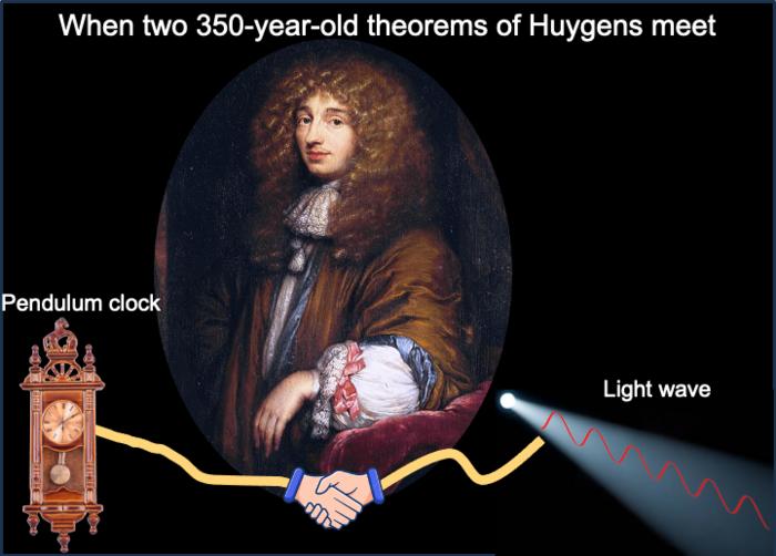
Caption: Physicists at Stevens Institute of Technology use a 350-year-old theorem that explains the workings of pendulums and planets to reveal new properties of light waves. Credit: Stevens Institute of Technology
An August 21, 2023 news item on phys.org revisits a 350-year old theorem, Note: Links have been removed,
Since the 17th century, when Isaac Newton and Christiaan Huygens first debated the nature of light, scientists have been puzzling over whether light is best viewed as a wave or a particle—or perhaps, at the quantum level, even both at once. Now, researchers at Stevens Institute of Technology have revealed a new connection between the two perspectives, using a 350-year-old mechanical theorem—ordinarily used to describe the movement of large, physical objects like pendulums and planets—to explain some of the most complex behaviors of light waves.
The work, led by Xiaofeng Qian, assistant professor of physics at Stevens and reported in the August 17 [2023] online issue of Physical Review Research, also proves for the first time that a light wave’s degree of non-quantum entanglement exists in a direct and complementary relationship with its degree of polarization. As one rises, the other falls, enabling the level of entanglement to be inferred directly from the level of polarization, and vice versa. This means that hard-to-measure optical properties such as amplitudes, phases and correlations—perhaps even these of quantum wave systems—can be deduced from something a lot easier to measure: light intensity.
“We’ve known for over a century that light sometimes behaves like a wave, and sometimes like a particle, but reconciling those two frameworks has proven extremely difficult,” said Qian “Our work doesn’t solve that problem — but it does show that there are profound connections between wave and particle concepts not just at the quantum level, but at the level of classical light-waves and point-mass systems.”
Qian’s team used a mechanical theorem, originally developed by Huygens in a 1673 book on pendulums, that explains how the energy required to rotate an object varies depending on the object’s mass and the axis around which it turns. “This is a well-established mechanical theorem that explains the workings of physical systems like clocks or prosthetic limbs,” Qian explained. “But we were able to show that it can offer new insights into how light works, too.”
This 350-year-old theorem describes relationships between masses and their rotational momentum, so how could it be applied to light where there is no mass to measure? Qian’s team interpreted the intensity of a light as the equivalent of a physical object’s mass, then mapped those measurements onto a coordinate system that could be interpreted using Huygens’ mechanical theorem. “Essentially, we found a way to translate an optical system so we could visualize it as a mechanical system, then describe it using well-established physical equations,” explained Qian.
Once the team visualized a light wave as part of a mechanical system, new connections between the wave’s properties immediately became apparent — including the fact that entanglement and polarization stood in a clear relationship with one another.
“This was something that hadn’t been shown before, but that becomes very clear once you map light’s properties onto a mechanical system,” said Qian. “What was once abstract becomes concrete: using mechanical equations, you can literally measure the distance between ‘center of mass’ and other mechanical points to show how different properties of light relate to one another.”
Clarifying these relationships could have important practical implications, allowing subtle and hard-to-measure properties of optical systems — or even quantum systems — to be deduced from simpler and more robust measurements of light intensity, Qian explained. More speculatively, the team’s findings suggest the possibility of using mechanical systems to simulate and better-understand the strange and complex behaviors of quantum wave systems.
“That still lies ahead of us, but with this first study we’ve shown clearly that by applying mechanical concepts, it’s possible to understand optical systems in an entirely new way,” Qian said. “Ultimately, this research is helping to simplify the way we understand the world, by allowing us to recognize the intrinsic underlying connections between apparently unrelated physical laws.”
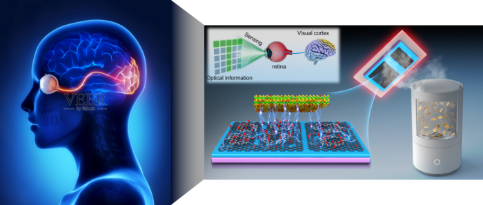
Researchers have created a small device that ‘sees’ and creates memories in a similar way to humans, in a promising step towards one day having applications that can make rapid, complex decisions such as in self-driving cars.
The neuromorphic invention is a single chip enabled by a sensing element, doped indium oxide, that’s thousands of times thinner than a human hair and requires no external parts to operate.
RMIT University engineers in Australia led the work, with contributions from researchers at Deakin University and the University of Melbourne.
The team’s research demonstrates a working device that captures, processes and stores visual information. With precise engineering of the doped indium oxide, the device mimics a human eye’s ability to capture light, pre-packages and transmits information like an optical nerve, and stores and classifies it in a memory system like the way our brains can.
Collectively, these functions could enable ultra-fast decision making, the team says.
Team leader Professor Sumeet Walia said the new device can perform all necessary functions – sensing, creating and processing information, and retaining memories – rather than relying on external energy-intensive computation, which prevents real-time decision making.
“Performing all of these functions on one small device had proven to be a big challenge until now,” said Walia from RMIT’s School of Engineering.
“We’ve made real-time decision making a possibility with our invention, because it doesn’t need to process large amounts of irrelevant data and it’s not being slowed down by data transfer to separate processors.”
What did the team achieve and how does the technology work?
The new device was able to demonstrate an ability to retain information for longer periods of time, compared to previously reported devices, without the need for frequent electrical signals to refresh the memory. This ability significantly reduces energy consumption and enhances the device’s performance.
Their findings and analysis are published in Advanced Functional Materials.
First author and RMIT PhD researcher Aishani Mazumder said the human brain used analog processing, which allowed it to process information quickly and efficiently using minimal energy.
“By contrast, digital processing is energy and carbon intensive, and inhibits rapid information gathering and processing,” she said.
“Neuromorphic vision systems are designed to use similar analog processing to the human brain, which can greatly reduce the amount of energy needed to perform complex visual tasks compared with today’s technologies
What are the potential applications?
The team used ultraviolet light as part of their experiments, and are working to expand this technology even further for visible and infrared light – with many possible applications such as bionic vision, autonomous operations in dangerous environments, shelf-life assessments of food and advanced forensics.
“Imagine a self-driving car that can see and recognise objects on the road in the same way that a human driver can or being able to able to rapidly detect and track space junk. This would be possible with neuromorphic vision technology.”
Walia said neuromorphic systems could adapt to new situations over time, becoming more efficient with more experience.
“Traditional computer vision systems – which cannot be miniaturised like neuromorphic technology – are typically programmed with specific rules and can’t adapt as easily,” he said.
“Neuromorphic robots have the potential to run autonomously for long periods, in dangerous situations where workers are exposed to possible cave-ins, explosions and toxic air.”
The human eye has a single retina that captures an entire image, which is then processed by the brain to identify objects, colours and other visual features.
The team’s device mimicked the retina’s capabilities by using single-element image sensors that capture, store and process visual information on one platform, Walia said.
“The human eye is exceptionally adept at responding to changes in the surrounding environment in a faster and much more efficient way than cameras and computers currently can,” he said.
“Taking inspiration from the eye, we have been working for several years on creating a camera that possesses similar abilities, through the process of neuromorphic engineering.”
A June 5, 2023 news item on Nanowerk announced a paper which reviews the state-of-the-art of optical memristors, Note: Links have been removed,
AI, machine learning, and ChatGPT may be relatively new buzzwords in the public domain, but developing a computer that functions like the human brain and nervous system – both hardware and software combined – has been a decades-long challenge. Engineers at the University of Pittsburgh are today exploring how optical “memristors” may be a key to developing neuromorphic computing.
Resistors with memory, or memristors, have already demonstrated their versatility in electronics, with applications as computational circuit elements in neuromorphic computing and compact memory elements in high-density data storage. Their unique design has paved the way for in-memory computing and captured significant interest from scientists and engineers alike.
A new review article published in Nature Photonics (“Integrated Optical Memristors”), sheds light on the evolution of this technology—and the work that still needs to be done for it to reach its full potential. Led by Nathan Youngblood, assistant professor of electrical and computer engineering at the University of Pittsburgh Swanson School of Engineering, the article explores the potential of optical devices which are analogs of electronic memristors. This new class of device could play a major role in revolutionizing high-bandwidth neuromorphic computing, machine learning hardware, and artificial intelligence in the optical domain.
“Researchers are truly captivated by optical memristors because of their incredible potential in high-bandwidth neuromorphic computing, machine learning hardware, and artificial intelligence,” explained Youngblood. “Imagine merging the incredible advantages of optics with local information processing. It’s like opening the door to a whole new realm of technological possibilities that were previously unimaginable.”
The review article presents a comprehensive overview of recent progress in this emerging field of photonic integrated circuits. It explores the current state-of-the-art and highlights the potential applications of optical memristors, which combine the benefits of ultrafast, high-bandwidth optical communication with local information processing. However, scalability emerged as the most pressing issue that future research should address.
“Scaling up in-memory or neuromorphic computing in the optical domain is a huge challenge. Having a technology that is fast, compact, and efficient makes scaling more achievable and would represent a huge step forward,” explained Youngblood.
“One example of the limitations is that if you were to take phase change materials, which currently have the highest storage density for optical memory, and try to implement a relatively simplistic neural network on-chip, it would take a wafer the size of a laptop to fit all the memory cells needed,” he continued. “Size matters for photonics, and we need to find a way to improve the storage density, energy efficiency, and programming speed to do useful computing at useful scales.”
Using Light to Revolutionize Computing
Optical memristors can revolutionize computing and information processing across several applications. They can enable active trimming of photonic integrated circuits (PICs), allowing for on-chip optical systems to be adjusted and reprogrammed as needed without continuously consuming power. They also offer high-speed data storage and retrieval, promising to accelerate processing, reduce energy consumption, and enable parallel processing.
Optical memristors can even be used for artificial synapses and brain-inspired architectures. Dynamic memristors with nonvolatile storage and nonlinear output replicate the long-term plasticity of synapses in the brain and pave the way for spiking integrate-and-fire computing architectures.
Research to scale up and improve optical memristor technology could unlock unprecedented possibilities for high-bandwidth neuromorphic computing, machine learning hardware, and artificial intelligence.
“We looked at a lot of different technologies. The thing we noticed is that we’re still far away from the target of an ideal optical memristor–something that is compact, efficient, fast, and changes the optical properties in a significant manner,” Youngblood said. “We’re still searching for a material or a device that actually meets all these criteria in a single technology in order for it to drive the field forward.”
The publication of “Integrated Optical Memristors” (DOI: 10.1038/s41566-023-01217-w) was published in Nature Photonics and is coauthored by senior author Harish Bhaskaran at the University of Oxford, Wolfram Pernice at Heidelberg University, and Carlos Ríos at the University of Maryland.
Despite including that final paragraph, I’m also providing a link to and a citation for the paper,
Integrated optical memristors by Nathan Youngblood, Carlos A. Ríos Ocampo, Wolfram H. P. Pernice & Harish Bhaskaran. Nature Photonics volume 17, pages 561–572 (2023) DOI: https://doi.org/10.1038/s41566-023-01217-w Published online: 29 May 2023 Issue Date: July 2023
A May 24, 2023 news item on phys.org introduces organic-inorganic nanohybrids for optoelectronic devices,
When designing optoelectronic devices, such as solar cells, photocatalysts, and photodetectors, scientists usually prioritize materials that are stable and possess tunable properties. This allows them precise control over optical characteristics of the materials and ensures retention of their properties over time, despite varying environmental conditions.
Organic-inorganic nanohybrids, which are made up of organic ligands attached to the surface of colloidal inorganic nanocrystals via coordinate bonds, are promising in this regard. They are known to exhibit enhanced stability owing to the formation of a protective layer by organic ligands around the reactive inorganic nanocrystal. However, the incorporation of organic ligands has been found to lower the conductivity and photon absorption efficiency of inorganic nanocrystals.
In a breakthrough study on ligand-nanocrystal interactions, researchers from Japan now demonstrate a quasi-reversible displacement of organic ligands on the surface of nanocrystals. Their findings, published in ACS Nano, provide a new perspective to the common belief that the organic ligands are anchored to the surface of the nanocrystals.
… The research team, led by Professor Yoichi Kobayashi from Ritsumeikan University, Japan, found that the coordination bond between perylene bisimide with a carboxyl group (PBI) and inorganic zinc sulfide (ZnS) nanocrystals can be reversibly displaced by exposing the material to visible light.
Shedding light on this novel behavior of organic-inorganic nanohybrids, Prof. Kobayashi says, “We explored the ligand properties of organic-inorganic nanohybrid systems by using perylene bisimide with a carboxyl group (PBI)-coordinated zinc sulfide (ZnS) NCs (PBI–ZnS) as a model system. Our findings provide the first example of photoinduced displacement of aromatic ligands with semiconductor nanocrystals.”
In their study, the researchers carried out both theoretical analysis and experimental investigations to understand the material’s unique photoinducible characteristics. They first conducted density functional theory calculations to study the structure and orbitals of PBI–ZnS ([PBI-Zn25S31]–) in both its ground and first excited states. Next, they performed time-resolved impulsive stimulated Raman spectroscopy to excite the sample with an ultrafast laser. This helped them analyze the corresponding Raman spectrum that revealed the nature of the excited state of PBI–ZnS.
The experimental observations and calculations showed that, upon photoexcitation, an electron is excited from the PBI molecule, and the corresponding “hole”(the vacancy formed due to the absence of the electron) rapidly moves from the aromatic ligand (PBI) to ZnS. This results in a long-lived, negatively-charged PBI ion that is displaced from the surface of the ZnS nanocrystal. Over time, however, the displaced ligands recombine with the surface defects of the ZnS nanocrystal, leading to a quasi-reversible photoinduced displacement of coordinated PBI. Notably, the dynamic behavior of coordinated ligand molecules observed in this study is different from that observed for typical photoinduced charge transfer processes in which the hole typically remains on the donor molecule, enabling it to recombine with the electron quickly.
Explaining the significance of these findings, Prof. Kobayashi says, “The precise understanding of ligand-nanocrystal interaction is important not only for fundamental nanoscience but also for developing advanced photofunctional materials using nanomaterials. These include photocatalysts for the decomposition of persistent chemicals using visible light and photoconductive microcircuit patterning for wearable devices.”
Indeed, the results of this study present a promising avenue for enhancing the tunability and functionality of inorganic materials with aromatic molecules. This, in turn, could significantly impact the field of fundamental nanoscience and photochemistry in the times to come.
Credit: by Xiao Fu, Tangxin Li, Bin Caid, Jinshui Miao, Gennady N. Panin, Xinyu Ma, Jinjin Wang, Xiaoyong Jiang, Qing Lia, Yi Dong, Chunhui Hao, Juyi Sun, Hangyu Xu, Qixiao Zhao, Mengjia Xia, Bo Song, Fansheng Chen, Xiaoshuang Chen, Wei Lu, Weida Hu
it took a while to get there but the February 13, 2023 news item on phys.org announced research into extending memristors from tunable conductance to reconfigurable photo-response,
In traditional vision systems, the optical information is captured by a frame-based digital camera, and then the digital signal is processed afterwards using machine-learning algorithms. In this scenario, a large amount of data (mostly redundant) has to be transferred from a standalone sensing elements to the processing units, which leads to high latency and power consumption.
To address this problem, much effort has been devoted to developing an efficient approach, where some of the memory and computational tasks are offloaded to sensor elements that can perceive and process the optical signal simultaneously.
In a new paper published in Light: Science & Applications, a team of scientists, led by Professor Weida Hu from School of Physics and Optoelectronic Engineering, Hangzhou Institute for Advanced Study, University of Chinese Academy of Sciences, Hangzhou, China, State Key Laboratory of Infrared Physics, Shanghai Institute of Technical Physics, Chinese Academy of Sciences, Shanghai, China, and co-workers have developed a non-volatile photo-memristor, in which the reconfigurable responsivity can be modulated by the charge and/or photon flux through it and further stored in the device.
The non-volatile photo-memristor has a simple two-terminal architecture, in which photoexcited carriers and oxygen-related ions are coupled, leading to a displaced and pinched hysteresis in the current-voltage characteristics. For the first time, non-volatile photo-memristors implement computationally complete logic with photoresponse-stateful operations, for which the same photo-memristor serves as both a logic gate and memory, using photoresponse as a physical state variable instead of light, voltage and memresistance. Polarity reversal of photo-memristors shows great potential for in-memory sensing and computing with feature extraction and image recognition for neuromorphic vision.
The photo-memristor demonstrates tunable short-circuit current in a non-volatile mode under illumination. By mimicking the biological functionalities of the human retina and designing specific device structures, the devices can act as neural network for neuromorphic visual processing and implementation of completely photoresponse-stateful logic operations triggered by electrical and light stimuli together. It can support various kinds of sensing tasks with all-in-one sensing-memory-computing approaches. These scientists summarize the operational principle and feature of their device:
“We design[ed] a two-terminal device with MoS2-xOx and specific graphene for three purposes in one: (1) to provide low barrier energy for the migration of oxygen ions; (2) to perform as geometry-asymmetric metal–semiconductor–metal van der Waals heterostructures with multi-photoresponse states; and (3) as an extension of a memristor, this device not only provides tunable conductance, but also demonstrates reconfigurable photoresponse for reading at zero bias voltage.”
“Moreover, the tunable short-circuit photocurrent and photoresponse can be increased to 889.8 nA and 98.8 mA/W, respectively, which are much higher than that of other reconfigurable phototransistors based on 2D materials. To reverse the channel polarity and obtain a gate-tunable short-circuit photocurrent, the channel semiconductor must be thin enough. Thus, it is difficult to use the thick film needed to absorb enough light to get a large signal. In our case, the mechanism of the two-terminal device rearrangement is based on ion migration, which is not limited by the thickness. We can increase the thickness of the film to absorb more photons and get a large short-circuit photocurrent.” they added.
“This new concept of a two-terminal photo-memristor not only enables all-in-one sensing-memory-computing approaches for neuromorphic vision hardware, but also brings great convenience for high-density integration.” the scientists forecast.
Here’s a link to and a citation for the paper,
Graphene/MoS2−xOx/graphene photomemristor with tunable non-volatile responsivities for neuromorphic vision processing by Xiao Fu, Tangxin Li, Bin Caid, Jinshui Miao, Gennady N. Panin, Xinyu Ma, Jinjin Wang, Xiaoyong Jiang, Qing Lia, Yi Dong, Chunhui Hao, Juyi Sun, Hangyu Xu, Qixiao Zhao, Mengjia Xia, Bo Song, Fansheng Chen, Xiaoshuang Chen, Wei Lu, Weida Hu. Light: Science & Applications volume 12, Article number: 39 (2023) DOI: https://doi.org/10.1038/s41377-023-01079-5 Published: 07 February 2023
Just when I think I’m getting caught up with my backlog along comes something like this. A February 21, 2023 news item on Nanowerk announces research that combines neuromorphic (brainlike) engineering and nanotechnology, Note: A link has been removed,
In a new study, researchers at the Indian Institute of Science (IISc) show how a brain-inspired image sensor can go beyond the diffraction limit of light to detect miniscule objects such as cellular components or nanoparticles invisible to current microscopes. Their novel technique, which combines optical microscopy with a neuromorphic camera and machine learning algorithms, presents a major step forward in pinpointing objects smaller than 50 nanometers in size.
Since the invention of optical microscopes, scientists have strived to surpass a barrier called the diffraction limit, which means that the microscope cannot distinguish between two objects if they are smaller than a certain size (typically 200-300 nanometers). Their efforts have largely focused on either modifying the molecules being imaged, or developing better illumination strategies – some of which led to the 2014 Nobel Prize in Chemistry. “But very few have actually tried to use the detector itself to try and surpass this detection limit,” says Deepak Nair, Associate Professor at the Centre for Neuroscience (CNS), IISc, and corresponding author of the study.
Measuring roughly 40 mm (height) by 60 mm (width) by 25 mm (diameter), and weighing about 100 grams, the neuromorphic camera used in the study mimics the way the human retina converts light into electrical impulses, and has several advantages over conventional cameras. In a typical camera, each pixel captures the intensity of light falling on it for the entire exposure time that the camera focuses on the object, and all these pixels are pooled together to reconstruct an image of the object. In neuromorphic cameras, each pixel operates independently and asynchronously, generating events or spikes only when there is a change in the intensity of light falling on that pixel. This generates sparse and lower amount of data compared to traditional cameras, which capture every pixel value at a fixed rate, regardless of whether there is any change in the scene. This functioning of a neuromorphic camera is similar to how the human retina works, and allows the camera to “sample” the environment with much higher temporal resolution – because it is not limited by a frame rate like normal cameras – and also perform background suppression.
“Such neuromorphic cameras have a very high dynamic range (>120 dB), which means that you can go from a very low-light environment to very high-light conditions. The combination of the asynchronous nature, high dynamic range, sparse data, and high temporal resolution of neuromorphic cameras make them well-suited for use in neuromorphic microscopy,” explains Chetan Singh Thakur, Assistant Professor at the Department of Electronic Systems Engineering (DESE), IISc, and co-author.
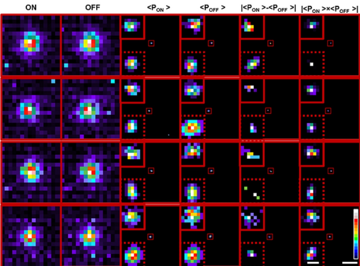
In the current study, the group used their neuromorphic camera to pinpoint individual fluorescent beads smaller than the limit of diffraction, by shining laser pulses at both high and low intensities, and measuring the variation in the fluorescence levels. As the intensity increases, the camera captures the signal as an “ON” event, while an “OFF” event is reported when the light intensity decreases. The data from these events were pooled together to reconstruct frames.
To accurately locate the fluorescent particles within the frames, the team used two methods. The first was a deep learning algorithm, trained on about one and a half million image simulations that closely represented the experimental data, to predict where the centroid of the object could be, explains Rohit Mangalwedhekar, former research intern at CNS and first author of the study. A wavelet segmentation algorithm was also used to determine the centroids of the particles separately for the ON and the OFF events. Combining the predictions from both allowed the team to zero in on the object’s precise location with greater accuracy than existing techniques.
“In biological processes like self-organisation, you have molecules that are alternating between random or directed movement, or that are immobilised,” explains Nair. “Therefore, you need to have the ability to locate the centre of this molecule with the highest precision possible so that we can understand the thumb rules that allow the self-organisation.” The team was able to closely track the movement of a fluorescent bead moving freely in an aqueous solution using this technique. This approach can, therefore, have widespread applications in precisely tracking and understanding stochastic processes in biology, chemistry and physics.
Caption: Transformation of cumulative probability density of ON and OFF processes allows localisation below the limit of classical single particle detection. Credit: Mangalwedhekar et al
Here’s a link to and a citation for the paper,
Achieving nanoscale precision using neuromorphic localization microscopy by Rohit Mangalwedhekar, Nivedita Singh, Chetan Singh Thakur, Chandra Sekhar Seelamantula, Mini Jose & Deepak Nair. Nature Nanotechnology volume 18, pages 380–389 (2023) DOI: https://doi.org/10.1038/s41565-022-01291-1 Published online: 23 January 2023 Issue Date: April 2023
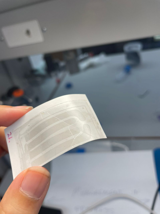
An April 17, 2023 news item on Nanowerk announced research into a graphene cardiac implant/tattoo,
Researchers led by Northwestern University and the University of Texas at Austin (UT) have developed the first cardiac implant made from graphene, a two-dimensional super material with ultra-strong, lightweight and conductive properties.
Similar in appearance to a child’s temporary tattoo, the new graphene “tattoo” implant is thinner than a single strand of hair yet still functions like a classical pacemaker. But unlike current pacemakers and implanted defibrillators, which require hard, rigid materials that are mechanically incompatible with the body, the new device softly melds to the heart to simultaneously sense and treat irregular heartbeats. The implant is thin and flexible enough to conform to the heart’s delicate contours as well as stretchy and strong enough to withstand the dynamic motions of a beating heart.
…
Caption: Graphene implant on tattoo paper. Credit: Ning Liu/University of Texas at Austin
After implanting the device into a rat model, the researchers demonstrated that the graphene tattoo could successfully sense irregular heart rhythms and then deliver electrical stimulation through a series of pulses without constraining or altering the heart’s natural motions. Even better: The technology also is optically transparent, allowing the researchers to use an external source of optical light to record and stimulate the heart through the device.
The study will be published on Thursday (April 20 [2023]) in the journal Advanced Materials. It marks the thinnest known cardiac implant to date.
“One of the challenges for current pacemakers and defibrillators is that they are difficult to affix onto the surface of the heart,” said Northwestern’s Igor Efimov, the study’s senior author. “Defibrillator electrodes, for example, are essentially coils made of very thick wires. These wires are not flexible, and they break. Rigid interfaces with soft tissues, like the heart, can cause various complications. By contrast, our soft, flexible device is not only unobtrusive but also intimately and seamlessly conforms directly onto the heart to deliver more precise measurements.”
An experimental cardiologist, Efimov is a professor of biomedical engineering at Northwestern’s McCormick School of Engineering and professor of medicine at Northwestern University Feinberg School of Medicine. He co-led the study with Dmitry Kireev, a research associate at UT. Zexu Lin, a Ph.D. candidate in Efimov’s laboratory, is the paper’s first author.
Miracle material
Known as cardiac arrhythmias, heart rhythm disorders occur when the heart beats either too quickly or too slowly. While some cases of arrhythmia are not serious, many cases can lead to heart failure, stroke and even sudden death. In fact, complications related to arrythmia claim about 300,000 lives annually in the United States. Physicians commonly treat arrhythmia with implantable pacemakers and defibrillators that detect abnormal heartbeats and then correct rhythm with electrical stimulation. While these devices are lifesaving, their rigid nature may constrain the heart’s natural motions, injure soft tissues, cause temporary discomfort and induce complications, such as painful swelling, perforations, blood clots, infection and more.
With these challenges in mind, Efimov and his team sought to develop a bio-compatible device ideal for conforming to soft, dynamic tissues. After reviewing multiple materials, the researchers settled on graphene, an atomically thin form of carbon. With its ultra-strong, lightweight structure and superior conductivity, graphene has potential for many applications in high-performance electronics, high-strength materials and energy devices.
“For bio-compatibility reasons, graphene is particularly attractive,” Efimov said. “Carbon is the basis of life, so it’s a safe material that is already used in different clinical applications. It also is flexible and soft, which works well as an interface between electronics and a soft, mechanically active organ.”
Hitting a beating target
At UT, study co-authors Dimitry Kireev and Deji Akinwande were already developing graphene electronic tattoos (GETs) with sensing capabilities. Flexible and weightless, their team’s e-tattoos adhere to the skin to continuously monitor the body’s vital signs, including blood pressure and the electrical activity of the brain, heart and muscles.
But, while the e-tattoos work well on the skin’s surface, Efimov’s team needed to investigate new methods to use these devices inside the body — directly onto the surface of the heart.
“It’s a completely different application scheme,” Efimov said. “Skin is relatively dry and easily accessible. Obviously, the heart is inside the chest, so it’s difficult to access and in a wet environment.”
The researchers developed an entirely new technique to encase the graphene tattoo and adhere it to the surface of a beating heart. First, they encapsulated the graphene inside a flexible, elastic silicone membrane — with a hole punched in it to give access to the interior graphene electrode. Then, they gently placed gold tape (with a thickness of 10 microns) onto the encapsulating layer to serve as an electrical interconnect between the graphene and the external electronics used to measure and stimulate the heart. Finally, they placed it onto the heart. The entire thickness of all layers together measures about 100 microns in total.
The resulting device was stable for 60 days on an actively beating heart at body temperature, which is comparable to the duration of temporary pacemakers used as bridges to permanent pacemakers or rhythm management after surgery or other therapies.
Optical opportunities
Leveraging the device’s transparent nature, Efimov and his team performed optocardiography — using light to track and modulate heart rhythm — in the animal study. Not only does this offer a new way to diagnose and treat heart ailments, the approach also opens new possibilities for optogenetics, a method to control and monitor single cells with light.
While electrical stimulation can correct a heart’s abnormal rhythm, optical stimulation is more precise. With light, researchers can track specific enzymes as well as interrogate specific heart, muscle or nerve cells.
“We can essentially combine electrical and optical functions into one biointerface,” Efimov said. “Because graphene is optically transparent, we can actually read through it, which gives us a much higher density of readout.”
A new cardiac implant made from graphene, a two-dimensional super material with ultra-strong, lightweight and conductive properties, functions like a classic pacemaker with some major improvements.
A team led by researchers from The University of Texas at Austin and Northwestern University developed the implantable derivative from wearable graphene-based electronic tattoo, or e-tattoo – graphene biointerface. The device, detailed in the journal Advanced Materials, marks the thinnest known cardiac implant to date.
“It’s very exciting to take our e-tattoo technology and use it as an implantable device inside the body,” said Dmitry Kireev, a postdoctoral research associate in the lab of professor Deji Akinwande’s lab at UT Austin who co-led the research. “The fact that is much more compatible with the human body, lightweight, and transparent, makes this a more natural solution for people dealing with heart problems.”
…
Hitting a beating target
At UT Austin, Akinwande and his team had been developing e-tattoos using graphene for several years, with a variety of functions, including monitoring body signals. Flexible and weightless, their team’s e-tattoos adhere to the skin to continuously monitor the body’s vital signs, including blood pressure and the electrical activity of the brain, heart and muscles.
But, while the e-tattoos work well on the skin’s surface, the researchers needed to find new ways to deploy these devices inside the body — directly onto the surface of the heart.
“The conditions inside the body are very different compared to affixing a device to the skin, so we had to re-imagine how we package our e-tattoo technology,” said Akinwande, a professor in the Chandra Family Department of Electrical and Computer Engineering.
The researchers developed an entirely new technique to encase the graphene tattoo and adhere it to the surface of a beating heart. …
Here’s a link to and a citation for the paper,
Graphene Biointerface for Cardiac Arrhythmia Diagnosis and Treatment by Zexu Lin, Dmitry Kireev, Ning Liu, Shubham Gupta, Jessica LaPiano, Sofian N. Obaid, Zhiyuan Chen, Deji Akinwande, Igor R. Efimov. Advanced Materials Volume 35, Issue 22 June 1, 2023 2212190 DOI: https://doi.org/10.1002/adma.202212190 First published online: 25 March 2023
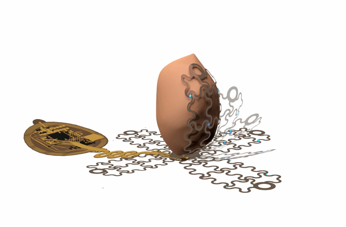
I think it looks more like a potato than a heart but it does illustrate how this new battery-free pacemaker would wrap around a heart,
Caption: An artist’s rendering shows how a new pacemaker, designed by a UArizona-led team of researchers, is able to envelop the heart. The wireless, battery-free pacemaker could be implanted with a less invasive procedure than currently possible and would cause patients less pain. Credit: Philipp Gutruff
An October 27, 2022 news item on ScienceDaily announces a technology that could make life much easier for people with pacemakers (Comment: In the image, that looks more like a potato than a heart, to me),
University of Arizona engineers lead a research team that is developing a new kind of pacemaker, which envelops the heart and uses precise targeting capabilities to bypass pain receptors and reduce patient discomfort.
Pacemakers are lifesaving devices that regulate the heartbeats of people with chronic heart diseases like atrial fibrillation and other forms of arrhythmia. However, pacemaker implantation is an invasive procedure, and the lifesaving pacing the devices provide can be extremely painful. Additionally, pacemakers can only be used to treat a few specific types of disease.
In a paper published Wednesday [October 26, 2022] in Science Advances, a University of Arizona-led team of researchers detail the workings of a wireless, battery-free pacemaker they designed that could be implanted with a less invasive procedure than currently possible and would cause patients less pain. The study was helmed by researchers in the Gutruf Lab, led by biomedical engineering assistant professor and Craig M. Berge Faculty Fellow Philipp Gutruf.
Currently available pacemakers work by implanting one or two leads, or points of contact, into the heart with hooks or screws. If the sensors on these leads detect a dangerous irregularity, they send an electrical shock through the heart to reset the beat.
“All of the cells inside the heart get hit at one time, including the pain receptors, and that’s what makes pacing or defibrillation painful,” Gutruf said. “It affects the heart muscle as a whole.”
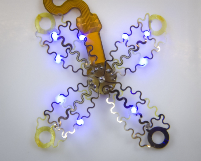
The device Gutruf’s team has developed, which has not yet been tested in humans, would allow pacemakers to send much more targeted signals using a new digitally manufactured mesh design that encompasses the entire heart. The device uses light and a technique called optogenetics.
Optogenetics modifies cells, usually neurons, sensitive to light, then uses light to affect the behavior of those cells. This technique only targets cardiomyocytes, the cells of the muscle that trigger contraction and make up the beat of the heart. This precision will not only reduce pain for pacemaker patients by bypassing the heart’s pain receptors, it will also allow the pacemaker to respond to different kinds of irregularities in more appropriate ways. For example, during atrial fibrillation, the upper and lower chambers of the heart beat asynchronously, and a pacemaker’s role is to get the two parts back in line.
“Whereas right now, we have to shock the whole heart to do this, these new devices can do much more precise targeting, making defibrillation both more effective and less painful,” said Igor Efimov, professor of biomedical engineering and medicine at Northwestern University, where the devices were lab-tested. “This technology could make life easier for patients all over the world, while also helping scientists and physicians learn more about how to monitor and treat the disease.”
Flexible mesh encompasses the heart
To ensure the light signals can reach many different parts of the heart, the team created a design that involves encompassing the organ, rather than implanting leads that provide limited points of contact.
The new pacemaker model consists of four petallike structures made of thin, flexible film, which contain light sources and a recording electrode. The petals, specially designed to accommodate the way the heart changes shape as it beats, fold up around the sides of the organ to envelop it, like a flower closing up at night.
“Current pacemakers record basically a simple threshold, and they will tell you, ‘This is going into arrhythmia, now shock!'” Gutruf said. “But this device has a computer on board where you can input different algorithms that allow you to pace in a more sophisticated way. It’s made for research.”
Because the system uses light to affect the heart, rather than electrical signals, the device can continue recording information even when the pacemaker needs to defibrillate. In current pacemakers, the electrical signal from the defibrillation can interfere with recording capabilities, leaving physicians with an incomplete picture of cardiac episodes. Additionally, the device does not require a battery, which could save pacemaker patients from needing to replace the battery in their device every five to seven years, as is currently the norm.
Gutruf’s team collaborated with researchers at Northwestern University on the project. While the current version of the device has been successfully demonstrated in animal models, the researchers look forward to furthering their work, which could improve the quality of life for millions of people.
The prototype looks like this,
Caption: The device uses light and a technique called optogenetics, which modifies cells that are sensitive to light, then uses light to affect the behavior of those cells.. Credit: Philipp Gutruff
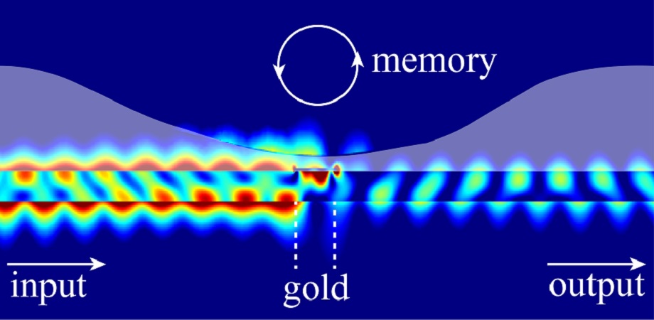
Simulation result of light affecting liquid geometry, which in turn affects reflection and transmission properties of the optical mode, thus constituting a two-way light–liquid interaction mechanism. The degree of deformation serves as an optical memory allowing to store the power magnitude of the previous optical pulse and use fluid dynamics to affect the subsequent optical pulse at the same actuation region, thus constituting an architecture where memory is part of the computation process. Credit: Gao et al., doi 10.1117/1.AP.4.4.046005
This is a fascinating approach to neuromorphic (brainlike) computing and given my recent post (August 29, 2022) about human cells being incorporated into computer chips, it’s part o my recent spate of posts about neuromorphic computing. From a July 25, 2022 news item on phys.org,
Sunlight sparkling on water evokes the rich phenomena of liquid-light interaction, spanning spatial and temporal scales. While the dynamics of liquids have fascinated researchers for decades, the rise of neuromorphic computing has sparked significant efforts to develop new, unconventional computational schemes based on recurrent neural networks, crucial to supporting wide range of modern technological applications, such as pattern recognition and autonomous driving. As biological neurons also rely on a liquid environment, a convergence may be attained by bringing nanoscale nonlinear fluid dynamics to neuromorphic computing.
Researchers from University of California San Diego recently proposed a novel paradigm where liquids, which usually do not strongly interact with light on a micro- or nanoscale, support significant nonlinear response to optical fields. As reported in Advanced Photonics, the researchers predict a substantial light–liquid interaction effect through a proposed nanoscale gold patch operating as an optical heater and generating thickness changes in a liquid film covering the waveguide.
The liquid film functions as an optical memory. Here’s how it works: Light in the waveguide affects the geometry of the liquid surface, while changes in the shape of the liquid surface affect the properties of the optical mode in the waveguide, thus constituting a mutual coupling between the optical mode and the liquid film. Importantly, as the liquid geometry changes, the properties of the optical mode undergo a nonlinear response; after the optical pulse stops, the magnitude of liquid film’s deformation indicates the power of the previous optical pulse.
Remarkably, unlike traditional computational approaches, the nonlinear response and the memory reside at the same spatial region, thus suggesting realization of a compact (beyond von-Neumann) architecture where memory and computational unit occupy the same space. The researchers demonstrate that the combination of memory and nonlinearity allow the possibility of “reservoir computing” capable of performing digital and analog tasks, such as nonlinear logic gates and handwritten image recognition.
Their model also exploits another significant liquid feature: nonlocality. This enables them to predict computation enhancement that is simply not possible in solid state material platforms with limited nonlocal spatial scale. Despite nonlocality, the model does not quite achieve the levels of modern solid-state optics-based reservoir computing systems, yet the work nonetheless presents a clear roadmap for future experimental works aiming to validate the predicted effects and explore intricate coupling mechanisms of various physical processes in a liquid environment for computation.
Using multiphysics simulations to investigate coupling between light, fluid dynamics, heat transport, and surface tension effects, the researchers predict a family of novel nonlinear and nonlocal optical effects. They go a step further by indicating how these can be used to realize versatile, nonconventional computational platforms. Taking advantage of a mature silicon photonics platform, they suggest improvements to state-of-the-art liquid-assisted computation platforms by around five orders magnitude in space and at least two orders of magnitude in speed.