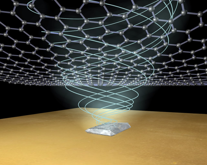
By pressure cooking birch leaves picked on campus the scientists produced carbon particles that can be used as raw material for the production of organic semiconductors. Image: Mattias Pettersson
Today, petrochemical compounds and rare metals such as platinum and iridium are used to produce semiconductors for optoelectronics, such as organic LEDs for super-thin TV and mobile phone screens. Physicists at Umeå University in collaboration with researchers in Denmark and China, have discovered a more sustainable alternative. By pressure-cooking birch leaves picked on the Umeå University campus, they have produced a nanosized carbon particle with desired optical properties.
“The essence of our research is to harness nearby renewable resources for producing organic semiconductor materials” says Jia Wang, research fellow at the Department of Physics, Umeå University, and one of the authors of the study that has been published in the Green Chemistry.
Organic semiconductors are one of the most important functional materials in optoelectronic applications. One example is the organic light-emitting diodes, OLEDs, which enable ultra-thin and bright TV and mobile phone screens. Sharply increasing demand for this advanced technology is driving massive production of organic semiconductor materials.
Unfortunately, these semiconductors are currently produced mainly from petrochemical compounds and rare elements, obtained through environmentally harmful mining. Moreover, these materials often contain so-called ‘critical raw materials’ that are in short supply, such as Platinum, Indium and Phosphorus.
From a sustainability point of view, it would be ideal if we can use biomass from plants, animals and waste to produce organic semiconductor materials. These starting materials are renewable and abundantly available. Research fellow Jia Wang and her colleagues at the Department of Physics, together with international partners, have succeeded in producing such a bio-based semiconductor material.
Birch leaves in pressure cooker
The synthesis process is simple: they picked birch leaves on the Umeå campus and cooked them in a pressure cooker. That produced a kind of ‘carbon dots’ about two nanometers in size, which emit a narrow-band, deep red light when dissolved in ethanol. Some of the optical properties of these birch leaf carbon dots are comparable to commercial quantum dots currently used in semiconductor materials, but unlike them, they contain no heavy metals or critical raw materials.
”It is important to note that our method is not limited to birch leaves” explains Jia Wang. “We tested different plant leaves with the same pressure cooking method, and all of them produced similar red-emitting carbon dots. This versatility suggests that the transformation process can be used in different locations.”
Using the carbon dots in a light-emitting electrochemical cell device, the researchers were able to show that the brightness generated was 100 cd/m2, which is comparable to the light intensity from a computer screen.
“It is important to note that our method is not limited to birch leaves.”
”This result shows that it is possible to transition from depleting petroleum compounds to regenerating biomass as a raw material for organic semiconductors” says Jia Wang.
She emphasises the broader potential of carbon dots beyond just light-emitting devices.
“Carbon dots are promising across various applications, from bioimaging and sensing to anti-counterfeiting. We’re open to collaborations and eager to explore more exciting uses for these emissive and sustainable carbon dots” says Jia Wang.
Here’s a link to and a citation for the paper,
Fluorescent carbon dots from birch leaves for sustainable electroluminescent devices by Shi Tang, Yongfeng Liu, Henry Opoku, Märta Gregorsson, Peijuan Zhang, Etienne Auroux, Dongfeng Dang, Anja-Verena Mudring, Thomas Wågberg, Ludvig Edman, and Jia Wang. Green Chem., 2023, 25, 9884-9895 DOI: https://doi.org/10.1039/D3GC03827K First published: 01 Nov 2023
Researchers have created a small device that ‘sees’ and creates memories in a similar way to humans, in a promising step towards one day having applications that can make rapid, complex decisions such as in self-driving cars.
The neuromorphic invention is a single chip enabled by a sensing element, doped indium oxide, that’s thousands of times thinner than a human hair and requires no external parts to operate.
RMIT University engineers in Australia led the work, with contributions from researchers at Deakin University and the University of Melbourne.
The team’s research demonstrates a working device that captures, processes and stores visual information. With precise engineering of the doped indium oxide, the device mimics a human eye’s ability to capture light, pre-packages and transmits information like an optical nerve, and stores and classifies it in a memory system like the way our brains can.
Collectively, these functions could enable ultra-fast decision making, the team says.
Team leader Professor Sumeet Walia said the new device can perform all necessary functions – sensing, creating and processing information, and retaining memories – rather than relying on external energy-intensive computation, which prevents real-time decision making.
“Performing all of these functions on one small device had proven to be a big challenge until now,” said Walia from RMIT’s School of Engineering.
“We’ve made real-time decision making a possibility with our invention, because it doesn’t need to process large amounts of irrelevant data and it’s not being slowed down by data transfer to separate processors.”
What did the team achieve and how does the technology work?
The new device was able to demonstrate an ability to retain information for longer periods of time, compared to previously reported devices, without the need for frequent electrical signals to refresh the memory. This ability significantly reduces energy consumption and enhances the device’s performance.
Their findings and analysis are published in Advanced Functional Materials.
First author and RMIT PhD researcher Aishani Mazumder said the human brain used analog processing, which allowed it to process information quickly and efficiently using minimal energy.
“By contrast, digital processing is energy and carbon intensive, and inhibits rapid information gathering and processing,” she said.
“Neuromorphic vision systems are designed to use similar analog processing to the human brain, which can greatly reduce the amount of energy needed to perform complex visual tasks compared with today’s technologies
What are the potential applications?
The team used ultraviolet light as part of their experiments, and are working to expand this technology even further for visible and infrared light – with many possible applications such as bionic vision, autonomous operations in dangerous environments, shelf-life assessments of food and advanced forensics.
“Imagine a self-driving car that can see and recognise objects on the road in the same way that a human driver can or being able to able to rapidly detect and track space junk. This would be possible with neuromorphic vision technology.”
Walia said neuromorphic systems could adapt to new situations over time, becoming more efficient with more experience.
“Traditional computer vision systems – which cannot be miniaturised like neuromorphic technology – are typically programmed with specific rules and can’t adapt as easily,” he said.
“Neuromorphic robots have the potential to run autonomously for long periods, in dangerous situations where workers are exposed to possible cave-ins, explosions and toxic air.”
The human eye has a single retina that captures an entire image, which is then processed by the brain to identify objects, colours and other visual features.
The team’s device mimicked the retina’s capabilities by using single-element image sensors that capture, store and process visual information on one platform, Walia said.
“The human eye is exceptionally adept at responding to changes in the surrounding environment in a faster and much more efficient way than cameras and computers currently can,” he said.
“Taking inspiration from the eye, we have been working for several years on creating a camera that possesses similar abilities, through the process of neuromorphic engineering.”
A May 24, 2023 news item on phys.org introduces organic-inorganic nanohybrids for optoelectronic devices,
When designing optoelectronic devices, such as solar cells, photocatalysts, and photodetectors, scientists usually prioritize materials that are stable and possess tunable properties. This allows them precise control over optical characteristics of the materials and ensures retention of their properties over time, despite varying environmental conditions.
Organic-inorganic nanohybrids, which are made up of organic ligands attached to the surface of colloidal inorganic nanocrystals via coordinate bonds, are promising in this regard. They are known to exhibit enhanced stability owing to the formation of a protective layer by organic ligands around the reactive inorganic nanocrystal. However, the incorporation of organic ligands has been found to lower the conductivity and photon absorption efficiency of inorganic nanocrystals.
In a breakthrough study on ligand-nanocrystal interactions, researchers from Japan now demonstrate a quasi-reversible displacement of organic ligands on the surface of nanocrystals. Their findings, published in ACS Nano, provide a new perspective to the common belief that the organic ligands are anchored to the surface of the nanocrystals.
… The research team, led by Professor Yoichi Kobayashi from Ritsumeikan University, Japan, found that the coordination bond between perylene bisimide with a carboxyl group (PBI) and inorganic zinc sulfide (ZnS) nanocrystals can be reversibly displaced by exposing the material to visible light.
Shedding light on this novel behavior of organic-inorganic nanohybrids, Prof. Kobayashi says, “We explored the ligand properties of organic-inorganic nanohybrid systems by using perylene bisimide with a carboxyl group (PBI)-coordinated zinc sulfide (ZnS) NCs (PBI–ZnS) as a model system. Our findings provide the first example of photoinduced displacement of aromatic ligands with semiconductor nanocrystals.”
In their study, the researchers carried out both theoretical analysis and experimental investigations to understand the material’s unique photoinducible characteristics. They first conducted density functional theory calculations to study the structure and orbitals of PBI–ZnS ([PBI-Zn25S31]–) in both its ground and first excited states. Next, they performed time-resolved impulsive stimulated Raman spectroscopy to excite the sample with an ultrafast laser. This helped them analyze the corresponding Raman spectrum that revealed the nature of the excited state of PBI–ZnS.
The experimental observations and calculations showed that, upon photoexcitation, an electron is excited from the PBI molecule, and the corresponding “hole”(the vacancy formed due to the absence of the electron) rapidly moves from the aromatic ligand (PBI) to ZnS. This results in a long-lived, negatively-charged PBI ion that is displaced from the surface of the ZnS nanocrystal. Over time, however, the displaced ligands recombine with the surface defects of the ZnS nanocrystal, leading to a quasi-reversible photoinduced displacement of coordinated PBI. Notably, the dynamic behavior of coordinated ligand molecules observed in this study is different from that observed for typical photoinduced charge transfer processes in which the hole typically remains on the donor molecule, enabling it to recombine with the electron quickly.
Explaining the significance of these findings, Prof. Kobayashi says, “The precise understanding of ligand-nanocrystal interaction is important not only for fundamental nanoscience but also for developing advanced photofunctional materials using nanomaterials. These include photocatalysts for the decomposition of persistent chemicals using visible light and photoconductive microcircuit patterning for wearable devices.”
Indeed, the results of this study present a promising avenue for enhancing the tunability and functionality of inorganic materials with aromatic molecules. This, in turn, could significantly impact the field of fundamental nanoscience and photochemistry in the times to come.
Photonic synapses with low power consumption and high sensitivity are expected to integrate sensing-memory-preprocessing capabilities
A new publication from Opto-Electronic Advances; DOI 10.29026/oea.2022.210069 discusses how photonic synapses with low power consumption and high sensitivity are expected to integrate sensing-memory-preprocessing capabilities.
Neuromorphic photonics/electronics is the future of ultralow energy intelligent computing and artificial intelligence (AI). In recent years, inspired by the human brain, artificial neuromorphic devices have attracted extensive attention, especially in simulating visual perception and memory storage. Because of its advantages of high bandwidth, high interference immunity, ultrafast signal transmission and lower energy consumption, neuromorphic photonic devices are expected to realize real-time response to input data. In addition, photonic synapses can realize non-contact writing strategy, which contributes to the development of wireless communication. The use of low-dimensional materials provides an opportunity to develop complex brain-like systems and low-power memory logic computers. For example, large-scale, uniform and reproducible transition metal dichalcogenides (TMDs) show great potential for miniaturization and low-power biomimetic device applications due to their excellent charge-trapping properties and compatibility with traditional CMOS processes. The von Neumann architecture with discrete memory and processor leads to high power consumption and low efficiency of traditional computing. Therefore, the sensor-memory fusion or sensor-memory- processor integration neuromorphic architecture system can meet the increasingly developing demands of big data and AI for low power consumption and high performance devices. Artificial synaptic devices are the most important components of neuromorphic systems. The performance evaluation of synaptic devices will help to further apply them to more complex artificial neural networks (ANN).
Chemical vapor deposition (CVD)-grown TMDs inevitably introduce defects or impurities, showed a persistent photoconductivity (PPC) effect. TMDs photonic synapses integrating synaptic properties and optical detection capabilities show great advantages in neuromorphic systems for low-power visual information perception and processing as well as brain memory.
The research Group of Optical Detection and Sensing (GODS) have reported a three-terminal photonic synapse based on the large-area, uniform multilayer MoS2 films. The reported device realized ultrashort optical pulse detection within 5 μs and ultralow power consumption about 40 aJ, which means its performance is much better than the current reported properties of photonic synapses. Moreover, it is several orders of magnitude lower than the corresponding parameters of biological synapses, indicating that the reported photonic synapse can be further used for more complex ANN. The photoconductivity of MoS2 channel grown by CVD is regulated by photostimulation signal, which enables the device to simulate short-term synaptic plasticity (STP), long-term synaptic plasticity (LTP), paired-pulse facilitation (PPF) and other synaptic properties. Therefore, the reported photonic synapse can simulate human visual perception, and the detection wavelength can be extended to near infrared light. As the most important system of human learning, visual perception system can receive 80% of learning information from the outside. With the continuous development of AI, there is an urgent need for low-power and high sensitivity visual perception system that can effectively receive external information. In addition, with the assistant of gate voltage, this photonic synapse can simulate the classical Pavlovian conditioning and the regulation of different emotions on memory ability. For example, positive emotions enhance memory ability and negative emotions weaken memory ability. Furthermore, a significant contrast in the strength of STP and LTP based on the reported photonic synapse suggests that it can preprocess the input light signal. These results indicate that the photo-stimulation and backgate control can effectively regulate the conductivity of MoS2 channel layer by adjusting carrier trapping/detrapping processes. Moreover, the photonic synapse presented in this paper is expected to integrate sensing-memory-preprocessing capabilities, which can be used for real-time image detection and in-situ storage, and also provides the possibility to break the von Neumann bottleneck.
I don’t have much to say about the research itself other than, I believe this is the first time I’ve seen a news release about neuromorphic computing research from China.
Group of Optical Detection and Sensing (GODS) [emphasis mine] was established in 2019. It is a research group focusing on compound semiconductors, lasers, photodetectors, and optical sensors. GODS has established a well-equipped laboratory with research facilities such as Molecular Beam Epitaxy system, IR detector test system, etc. GODS is leading several research projects funded by NSFC and National Key R&D Programmes. GODS have published more than 100 research articles in Nature Electronics, Light: Science and Applications, Advanced Materials and other international well-known high-level journals with the total citations beyond 8000.
Jiang Wu obtained his Ph.D. from the University of Arkansas Fayetteville in 2011. After his Ph.D., he joined UESTC as associate professor and later professor. He joined University College London [UCL] as a research associate in 2012 and then lecturer in the Department of Electronic and Electrical Engineering at UCL from 2015 to 2018. He is now a professor at UESTC [University of Electronic Science and Technology of China] [emphases mine]. His research interests include optoelectronic applications of semiconductor heterostructures. He is a Fellow of the Higher Education Academy and Senior Member of IEEE.
Opto-Electronic Advances (OEA) is a high-impact, open access, peer reviewed monthly SCI journal with an impact factor of 9.682 (Journals Citation Reports for IF 2020). Since its launch in March 2018, OEA has been indexed in SCI, EI, DOAJ, Scopus, CA and ICI databases over the time and expanded its Editorial Board to 36 members from 17 countries and regions (average h-index 49). [emphases mine]
The journal is published by The Institute of Optics and Electronics, Chinese Academy of Sciences, aiming at providing a platform for researchers, academicians, professionals, practitioners, and students to impart and share knowledge in the form of high quality empirical and theoretical research papers covering the topics of optics, photonics and optoelectronics.
The research group’s awkward name was almost certainly developed with the rather grandiose acronym, GODS, in mind. I don’t think you could get away with doing this in an English-speaking country as your colleagues would mock you mercilessly.
In a systematic evaluation of China’s Young Thousand Talents (YTT) program, which was established in 2010, researchers find that China has been successful in recruiting and nurturing high-caliber Chinese scientists who received training abroad. Many of these individuals outperform overseas peers in publications and access to funding, the study shows, largely due to access to larger research teams and better research funding in China. Not only do the findings demonstrate the program’s relative success, but they also hold policy implications for the increasing number of governments pursuing means to tap expatriates for domestic knowledge production and talent development. China is a top sender of international students to United States and European Union science and engineering programs. The YTT program was created to recruit and nurture the productivity of high-caliber, early-career, expatriate scientists who return to China after receiving Ph.Ds. abroad. Although there has been a great deal of international attention on the YTT, some associated with the launch of the U.S.’s controversial China Initiative and federal investigations into academic researchers with ties to China, there has been little evidence-based research on the success, impact, and policy implications of the program itself. Dongbo Shi and colleagues evaluated the YTT program’s first 4 cohorts of scholars and compared their research productivity to that of their peers that remained overseas. Shi et al. found that China’s YTT program successfully attracted high-caliber – but not top-caliber – scientists. However, those young scientists that did return outperformed others in publications across journal-quality tiers – particularly in last-authored publications. The authors suggest that this is due to YTT scholars’ greater access to larger research teams and better research funding in China. The authors say the dearth of such resources in the U.S. and E.U. “may not only expedite expatriates’ return decisions but also motivate young U.S.- and E.U.-born scientists to seek international research opportunities.” They say their findings underscore the need for policy adjustments to allocate more support for young scientists.
Kudos to the folks behind China’s Young Thousands Talents program! Jiang Wu’s career appears to be a prime example of the program’s success. Perhaps Canadian policy makers will be inspired.
An April 7, 2022 news item on Nanowerk announces graphene research that could lead to advances in optoelectronics (Note: Links have been removed),
An international team, co-led by researchers at The University of Manchester’s National Graphene Institute (NGI) in the UK and the Penn State [Pennsylvania State University] College of Engineering in the US, has developed a tunable graphene-based platform that allows for fine control over the interaction between light and matter in the terahertz (THz) spectrum to reveal rare phenomena known as exceptional points.
The team published their results in Science (“Topological engineering of terahertz light using electrically tuneable exceptional point singularities”).
The work could advance optoelectronic technologies to better generate, control and sense light and potentially communications, according to the researchers. They demonstrated a way to control THz waves, which exist at frequencies between those of microwaves and infrared waves. The feat could contribute to the development of ‘beyond-5G’ wireless technology for high-speed communication networks.
Light and matter can couple, interacting at different levels: weakly, where they might be correlated but do not change each other’s constituents; or strongly, where their interactions can fundamentally change the system. The ability to control how the coupling shifts from weak to strong and back again has been a major challenge to advancing optoelectronic devices — a challenge researchers have now solved.
“We have demonstrated a new class of optoelectronic devices using concepts of topology — a branch of mathematics studying properties of geometric objects,” said co-corresponding author Coskun Kocabas, professor of 2D device materials at The University of Manchester. “Using exceptional point singularities, we show that topological concepts can be used to engineer optoelectronic devices that enable new ways to manipulate terahertz light.”
Exceptional points are spectral singularities — points at which any two spectral values in an open system coalesce. They are, unsurprisingly, exceptionally sensitive and respond to even the smallest changes to the system, revealing curious yet desirable characteristics, according to co-corresponding author Şahin K. Özdemir, associate professor of engineering science and mechanics at Penn State.
“At an exceptional point, the energy landscape of the system is considerably modified, resulting in reduced dimensionality and skewed topology,” said Özdemir, who is also affiliated with the Materials Research Institute, Penn State. “This, in turn, enhances the system’s response to perturbations, modifies the local density of states leading to the enhancement of spontaneous emission rates and leads to a plethora of phenomena. Control of exceptional points, and the physical processes that occur at them, could lead to applications for better sensors, imaging, lasers and much more.”
Platform composition
The platform the researchers developed consists of a graphene-based tunable THz resonator, with a gold-foil gate electrode forming a bottom reflective mirror. Above it, a graphene layer is book-ended with electrodes, forming a tunable top mirror. A non-volatile ionic liquid electrolyte layer sits between the mirrors, enabling control of the top mirror’s reflectivity by changing the applied voltage. In the middle of the device, between the mirrors, are molecules of alpha lactose, a sugar commonly found in milk.
The system is controlled by two adjusters. One raises the lower mirror to change the length of the cavity — tuning the frequency of resonation to couple the light with the collective vibrational modes of the organic sugar molecules, which serve as a fixed number of oscillators for the system. The other adjuster changes the voltage applied to the top graphene mirror — altering the graphene’s reflective properties to transition the energy loss imbalances to adjust coupling strength. The delicate, fine tuning shifts weakly coupled terahertz light and organic molecules to become strongly coupled and vice versa.
“Exceptional points coincide with the crossover point between the weak and strong coupling regimes of terahertz light with collective molecular vibrations,” Özdemir said.
He noted that these singularity points are typically studied and observed in the coupling of analogous modes or systems, such as two optical modes, electronic modes or acoustic modes.
“This work is one of rare cases where exceptional points are demonstrated to emerge in the coupling of two modes with different physical origins,” Kocabas said. “Due to the topology of the exceptional points, we observed a significant modulation in the magnitude and phase of the terahertz light, which could find applications in next-generation THz communications.”
Unprecedented phase modulation in the THz spectrum
As the researchers apply voltage and adjust the resonance, they drive the system to an exceptional point and beyond. Before, at and beyond the exceptional point, the geometric properties — the topology — of the system change.
One such change is the phase modulation, which describes how a wave changes as it propagates and interacts in the THz field. Controlling the phase and amplitude of THz waves is a technological challenge, the researchers said, but their platform demonstrates unprecedented levels of phase modulation. The researchers moved the system through exceptional points, as well as along loops around exceptional points in different directions, and measured how it responded through the changes. Depending on the system’s topology at the point of measurement, phase modulation could range from zero to four magnitudes larger.
“We can electrically steer the device through an exceptional point, which enables electrical control on reflection topology,” said first author M. Said Ergoktas. “Only by controlling the topology of the system electronically could we achieve these huge modulations.”
According to the researchers, the topological control of light-matter interactions around an exceptional point enabled by the graphene-based platform has potential applications ranging from topological optoelectronic and quantum devices to topological control of physical and chemical processes.
Contributors include Kaiyuan Wang, Gokhan Bakan, Thomas B. Smith, Alessandro Principi and Kostya S. Novoselov, University of Manchester; Sina Soleymani, graduate student in the Penn State Department of Engineering Science and Mechanics; Sinan Balci, Izmir Institute of Technology, Turkey; Nurbek Kakenov, who conducted work for this paper while at Bilkent University, Turkey.
I love the language in this press release, especially, ‘spectral singularities’. The explanations are more appreciated and help to make this image more than a pretty picture,
Caption: An international team, co-led by researchers at The University of Manchester’s National Graphene Institute (NGI) in the UK and the Penn State College of Engineering in the US, has developed a tunable graphene-based platform that allows for fine control over the interaction between light and matter in the terahertz (THz) spectrum to reveal rare phenomena known as exceptional points. The feat could contribute to the development of beyond-5G wireless technology for high-speed communication networks. Credit: Image Design, Pietro Steiner, The University of Manchester
Oddly, there is an identical press release dated April 8, 2022 on the Pennsylvania State University website with a byline for By Ashley J. WennersHerron and Alan Beck. Interestingly the first author is from Penn State and the second author is from the University of Manchester.
Yes, it’s a ‘Top Gun’ movie quote (1986) or more accurately, a paraphrasing of Tom Cruise’s line “I feel the need for speed.” I understand there’s a sequel, which is due to arrive in movie theatres or elsewhere at sometime in this decade.
Where wireless and WiFi are concerned I think there is a dog/poodle situation. ‘Dog’ is a general description where ‘poodle’ is a specific description. All poodles (specific) are dogs (general) but not all dogs are poodles. So, wireless is a general description and Wi-Fi is a specific type of wireless communication. All WiFi is wireless but not all wireless is Wi-Fi. That said, onto the research.
Given what seems to be an insatiable desire for speed in the wireless world, the quote seems quite à propos in relation to the latest work on quantum tunneling and its impact on Wi-Fi speed from the Moscow Institute of Physics and Technology (from a February 3, 2021 news item on phys.org,
Scientists from MIPT (Moscow Institute of Physics and Technology), Moscow Pedagogical State University and the University of Manchester have created a highly sensitive terahertz detector based on the effect of quantum-mechanical tunneling in graphene. The sensitivity of the device is already superior to commercially available analogs based on semiconductors and superconductors, which opens up prospects for applications of the graphene detector in wireless communications, security systems, radio astronomy, and medical diagnostics. The research results are published in Nature Communications.
Information transfer in wireless networks is based on transformation of a high-frequency continuous electromagnetic wave into a discrete sequence of bits. This technique is known as signal modulation. To transfer the bits faster, one has to increase the modulation frequency. However, this requires synchronous increase in carrier frequency. A common FM-radio transmits at frequencies of hundred megahertz, a Wi-Fi receiver uses signals of roughly five gigahertz frequency, while the 5G mobile networks can transmit up to 20 gigahertz signals. This is far from the limit, and further increase in carrier frequency admits a proportional increase in data transfer rates. Unfortunately, picking up signals with hundred gigahertz frequencies and higher is an increasingly challenging problem.
A typical receiver used in wireless communications consists of a transistor-based amplifier of weak signals and a demodulator that rectifies the sequence of bits from the modulated signal. This scheme originated in the age of radio and television, and becomes inefficient at frequencies of hundreds of gigahertz desirable for mobile systems. The fact is that most of the existing transistors aren’t fast enough to recharge at such a high frequency.
An evolutionary way to solve this problem is just to increase the maximum operation frequency of a transistor. Most specialists in the area of nanoelectronics work hard in this direction. A revolutionary way to solve the problem was theoretically proposed in the beginning of 1990’s by physicists Michael Dyakonov and Michael Shur, and realized, among others, by the group of authors in 2018. It implies abandoning active amplification by transistor, and abandoning a separate demodulator. What’s left in the circuit is a single transistor, but its role is now different. It transforms a modulated signal into bit sequence or voice signal by itself, due to non-linear relation between its current and voltage drop.
In the present work, the authors have proved that the detection of a terahertz signal is very efficient in the so-called tunneling field-effect transistor. To understand its work, one can just recall the principle of an electromechanical relay, where the passage of current through control contacts leads to a mechanical connection between two conductors and, hence, to the emergence of current. In a tunneling transistor, applying voltage to the control contact (termed as ”gate”) leads to alignment of the energy levels of the source and channel. This also leads to the flow of current. A distinctive feature of a tunneling transistor is its very strong sensitivity to control voltage. Even a small “detuning” of energy levels is enough to interrupt the subtle process of quantum mechanical tunneling. Similarly, a small voltage at the control gate is able to “connect” the levels and initiate the tunneling current
“The idea of ??a strong reaction of a tunneling transistor to low voltages is known for about fifteen years,” says Dr. Dmitry Svintsov, one of the authors of the study, head of the laboratory for optoelectronics of two-dimensional materials at the MIPT center for photonics and 2D materials. “But it’s been known only in the community of low-power electronics. No one realized before us that the same property of a tunneling transistor can be applied in the technology of terahertz detectors. Georgy Alymov (co-author of the study) and I were lucky to work in both areas. We realized then: if the transistor is opened and closed at a low power of the control signal, then it should also be good in picking up weak signals from the ambient surrounding. “
The created device is based on bilayer graphene, a unique material in which the position of energy levels (more strictly, the band structure) can be controlled using an electric voltage. This allowed the authors to switch between classical transport and quantum tunneling transport within a single device, with just a change in the polarities of the voltage at the control contacts. This possibility is of extreme importance for an accurate comparison of the detecting ability of a classical and quantum tunneling transistor.
The experiment showed that the sensitivity of the device in the tunnelling mode is few orders of magnitude higher than that in the classical transport mode. The minimum signal distinguishable by the detector against the noisy background already competes with that of commercially available superconducting and semiconductor bolometers. However, this is not the limit – the sensitivity of the detector can be further increased in “cleaner” devices with a low concentration of residual impurities. The developed detection theory, tested by the experiment, shows that the sensitivity of the “optimal” detector can be a hundred times higher.
“The current characteristics give rise to great hopes for the creation of fast and sensitive detectors for wireless communications,” says the author of the work, Dr. Denis Bandurin. And this area is not limited to graphene and is not limited to tunnel transistors. We expect that, with the same success, a remarkable detector can be created, for example, based on an electrically controlled phase transition. Graphene turned out to be just a good launching pad here, just a door, behind which is a whole world of exciting new research.”
The results presented in this paper are an example of a successful collaboration between several research groups. The authors note that it is this format of work that allows them to obtain world-class scientific results. For example, earlier, the same team of scientists demonstrated how waves in the electron sea of ??graphene can contribute to the development of terahertz technology. “In an era of rapidly evolving technology, it is becoming increasingly difficult to achieve competitive results.” – comments Dr. Georgy Fedorov, deputy head of the nanocarbon materials laboratory, MIPT, – “Only by combining the efforts and expertise of several groups can we successfully realize the most difficult tasks and achieve the most ambitious goals, which we will continue to do.”
Here’s a link to and a citation for the latest paper,
Tunnel field-effect transistors for sensitive terahertz detection by I. Gayduchenko, S. G. Xu, G. Alymov, M. Moskotin, I. Tretyakov, T. Taniguchi, K. Watanabe, G. Goltsman, A. K. Geim, G. Fedorov, D. Svintsov & D. A. Bandurin. Nature Communications volume 12, Article number: 543 (2021) DOI: https://doi.org/10.1038/s41467-020-20721-z Published: 22 January 2021
This paper is open access.
One last comment, I’m assuming since the University of Manchester is mentioned that A. K. Geim is Sir Andre K. Geim (you can look him up here is you’re not familiar with his role in the graphene research community).
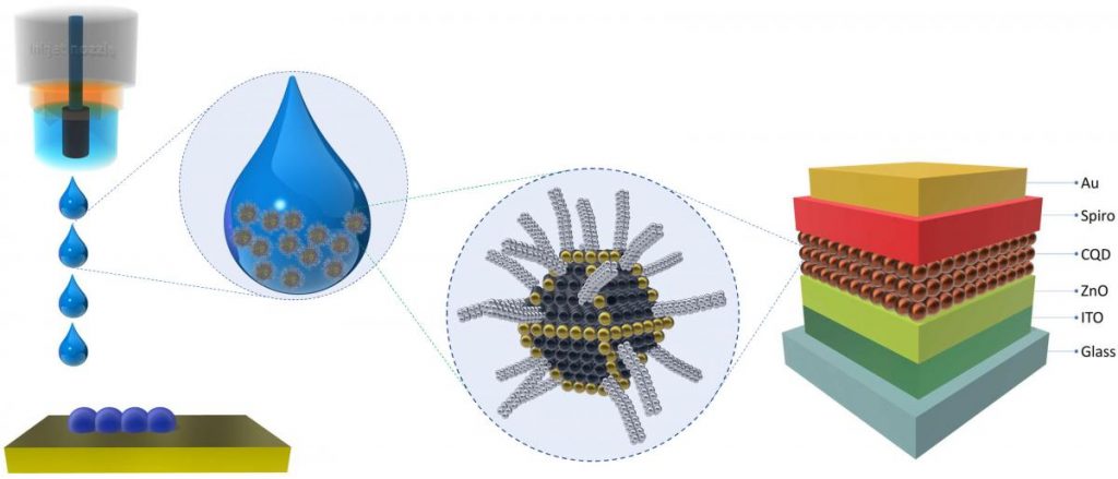
An October 16, 2019 news item on Nanowerk announces some of the latest work with colloidal quantum dots,
Researchers of the Optoelectronics and Measurement Techniques Unit (OPEM) at the University of Oulu [Finland] have invented a new method of producing ultra-sensitive hyper-spectral photodetectors. At the heart of the discovery are colloidal quantum dots, developed together with the researchers at the University of Toronto, Canada.
Quantum dots are tiny particles of 15-150 atoms of semiconducting material that have extraordinary optical and electrical properties due to quantum mechanics phenomena.
By controlling the size of the dots, the researchers are able to finetune how they react to different light colors (light wavelengths), especially those invisible for the human eye, namely the infrared spectrum.
…
The figure briefly introduces the concept of the study conducted by the researchers of the University of Oulu and the University of Toronto. The solution consisting of colloidal quantum dots is inkjet-printed, creating active photosensitive layer of the photodetector. Courtesy: Oulu University
-Naturally, it is very rewarding that our hard work has been recognized by the international scientific community but at the same time, this report helps us to realize that there is a long journey ahead in incoming years. This publication is especially satisfying because it is the result of collaboration with world-class experts at the University of Toronto, Canada. This international collaboration where we combined the expertise of Toronto’s researchers in synthesizing quantum dots and our expertise in printed intelligence resulted in truly unique devices with astonishing performance, says docent Rafal Sliz, a leading researcher in this project.
Mastered in the OPEM unit, inkjet printing technology makes possible the creation of optoelectronic devices by designing functional inks that are printed on various surfaces, for instance, flexible substrates, clothing or human skin. Inkjet printing combined with colloidal quantum dots allowed the creation of photodetectors of impresive detectivity characteristics. The developed technology is a milestone in the creation of a new type of sub-micron-thick, flexible, and inexpensive IR sensing devices, the next generation of solar cells and other novel photonic systems.
-Oulus’ engineers and scientists’ strong expertise in optoelectronics resulted in many successful Oulu-based companies like Oura, Specim, Focalspec, Spectral Engines, and many more. New optoelectronic technologies, materials, and methods developed by our researchers will help Oulu and Finland to stay at the cutting edge of innovation, says professor Tapio Fabritius, a leader of the OPEM.
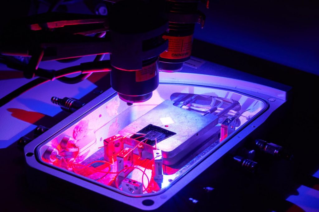
There are three (or more?) possible applications including neuromorphic computing for this new optoelectronic technology which is based on black phophorus. A July 16, 2019 news item on Nanowerk announces the research,
Researchers from RMIT University [Australia] drew inspiration from an emerging tool in biotechnology – optogenetics – to develop a device that replicates the way the brain stores and loses information.
Optogenetics allows scientists to delve into the body’s electrical system with incredible precision, using light to manipulate neurons so that they can be turned on or off.
The new chip is based on an ultra-thin material that changes electrical resistance in response to different wavelengths of light, enabling it to mimic the way that neurons work to store and delete information in the brain.
…
Caption: The new chip is based on an ultra-thin material that changes electrical resistance in response to different wavelengths of light. Credit: RMIT University
Research team leader Dr Sumeet Walia said the technology moves us closer towards artificial intelligence (AI) that can harness the brain’s full sophisticated functionality.
“Our optogenetically-inspired chip imitates the fundamental biology of nature’s best computer – the human brain,” Walia said.
“Being able to store, delete and process information is critical for computing, and the brain does this extremely efficiently.
“We’re able to simulate the brain’s neural approach simply by shining different colours onto our chip.
“This technology takes us further on the path towards fast, efficient and secure light-based computing.
“It also brings us an important step closer to the realisation of a bionic brain – a brain-on-a-chip that can learn from its environment just like humans do.”
Dr Taimur Ahmed, lead author of the study published in Advanced Functional Materials, said being able to replicate neural behavior on an artificial chip offered exciting avenues for research across sectors.
“This technology creates tremendous opportunities for researchers to better understand the brain and how it’s affected by disorders that disrupt neural connections, like Alzheimer’s disease and dementia,” Ahmed said.
The researchers, from the Functional Materials and Microsystems Research Group at RMIT, have also demonstrated the chip can perform logic operations – information processing – ticking another box for brain-like functionality.
Developed at RMIT’s MicroNano Research Facility, the technology is compatible with existing electronics and has also been demonstrated on a flexible platform, for integration into wearable electronics.
How the chip works:
Neural connections happen in the brain through electrical impulses. When tiny energy spikes reach a certain threshold of voltage, the neurons bind together – and you’ve started creating a memory.
On the chip, light is used to generate a photocurrent. Switching between colors causes the current to reverse direction from positive to negative.
This direction switch, or polarity shift, is equivalent to the binding and breaking of neural connections, a mechanism that enables neurons to connect (and induce learning) or inhibit (and induce forgetting).
This is akin to optogenetics, where light-induced modification of neurons causes them to either turn on or off, enabling or inhibiting connections to the next neuron in the chain.
To develop the technology, the researchers used a material called black phosphorus (BP) that can be inherently defective in nature.
This is usually a problem for optoelectronics, but with precision engineering the researchers were able to harness the defects to create new functionality.
“Defects are usually looked on as something to be avoided, but here we’re using them to create something novel and useful,” Ahmed said.
“It’s a creative approach to finding solutions for the technical challenges we face.”
Here’s a link and a citation for the paper,
Multifunctional Optoelectronics via Harnessing Defects in Layered Black Phosphorus by Taimur Ahmed, Sruthi Kuriakose, Sherif Abbas,, Michelle J. S. Spencer, Md. Ataur Rahman, Muhammad Tahir, Yuerui Lu, Prashant Sonar, Vipul Bansal, Madhu Bhaskaran, Sharath Sriram, Sumeet Walia. Advanced Functional Materials DOI: https://doi.org/10.1002/adfm.201901991 First published (online): 17 July 2019
Scientists at Japan’s University of Osaka have a technique for creating higher resolution computer and smart phone screens from the main ingredient for a dessert, nata de coco. From the nata de coco Wikipedia entry (Note: Links have been removed),
Nata de coco (also marketed as “coconut gel”) is a chewy, translucent, jelly-like food produced by the fermentation of coconut water,[1] which gels through the production of microbial cellulose by ‘Komagataeibacter xylinus’. Originating in the Philippines, nata de coco is most commonly sweetened as a candy or dessert, and can accompany a variety of foods, including pickles, drinks, ice cream, puddings, and fruit cocktails.[2]
A team at the Institute of Scientific and Industrial Research at Osaka University has determined the optical parameters of cellulose molecules with unprecedented precision. They found that cellulose’s intrinsic birefringence, which describes how a material reacts differently to light of various orientations, is powerful enough to be used in optical displays, such as flexible screens or electronic paper (ACS Macro Letters, “Estimation of the Intrinsic Birefringence of Cellulose Using Bacterial Cellulose Nanofiber Films”
An April 18, 2019 Osaka University press release on AlphaGalileo, which originated the news release, provides some historical context for the use of cellulose along with additional detail about the research,
Cellulose is an ancient material that may be poised for a major comeback. It has been utilized for millennia as the primary component of paper books, cotton clothing, and nata de coco, a tropical dessert made from coconut water. While books made of dead trees and plain old shirts might seem passé in world increasingly filled with tablets and smartphones, researchers at Osaka University have shown that cellulose might have just what it takes to make our modern electronic screens cheaper and provide sharper, more vibrant images.
Cellulose, a naturally occurring polymer, consists of many long molecular chains. Because of its rigidity and strength, cellulose helps maintain the structural integrity of the cell walls in plants. It makes up about 99% of the nanofibers that comprise nata de coco, and helps create its unique and tasty texture.
The team at Osaka University achieved better results using unidirectionally-aligned cellulose nanofiber films created by stretching hydrogels from nata de coco at various rates. Nata de coco nanofibers allow the cellulose chains to be straight on the molecular level, and this is helpful for the precise determination of the intrinsic birefringence–that is, the maximum birefringence of fully extended polymer chains. The researchers were also able to measure the birefringence more accurately through improvements in method. “Using high quality samples and methods, we were able to reliably determine the inherent birefringence of cellulose, for which very different values had been previously estimated,” says senior author Masaya Nogi.
The main application the researchers envision is as light compensation films for liquid crystal displays (LCDs), since they operate by controlling the brightness of pixels with filters that allow only one orientation of light to pass through. Potentially, any smartphone, computer, or television that has an LCD screen could see improved contrast, along with reduced color unevenness and light leakage with the addition of cellulose nanofiber films.
“Cellulose nanofibers are promising light compensation materials for optoelectronics, such as flexible displays and electronic paper, since they simultaneously have good transparency, flexibility, dimensional stability, and thermal conductivity,” says lead author Kojiro Uetani. “So look for this ancient material in your future high-tech devices.”
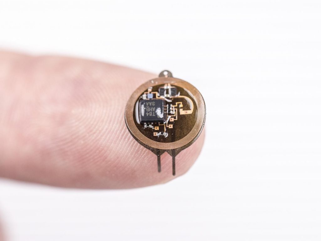
Caption: Wireless and battery-free implant with advanced control over targeted neuron groups. Credit: Philipp Gutruf
This January 2, 2019 news item on ScienceDaily describes the object seen in the above and describes the problem it’s designed to solve,
University of Arizona biomedical engineering professor Philipp Gutruf is first author on the paper Fully implantable, optoelectronic systems for battery-free, multimodal operation in neuroscience research, published in Nature Electronics.
Optogenetics is a biological technique that uses light to turn specific neuron groups in the brain on or off. For example, researchers might use optogenetic stimulation to restore movement in case of paralysis or, in the future, to turn off the areas of the brain or spine that cause pain, eliminating the need for — and the increasing dependence on — opioids and other painkillers.
“We’re making these tools to understand how different parts of the brain work,” Gutruf said. “The advantage with optogenetics is that you have cell specificity: You can target specific groups of neurons and investigate their function and relation in the context of the whole brain.”
In optogenetics, researchers load specific neurons with proteins called opsins, which convert light to electrical potentials that make up the function of a neuron. When a researcher shines light on an area of the brain, it activates only the opsin-loaded neurons.
The first iterations of optogenetics involved sending light to the brain through optical fibers, which meant that test subjects were physically tethered to a control station. Researchers went on to develop a battery-free technique using wireless electronics, which meant subjects could move freely.
But these devices still came with their own limitations — they were bulky and often attached visibly outside the skull, they didn’t allow for precise control of the light’s frequency or intensity, and they could only stimulate one area of the brain at a time.
“With this research, we went two to three steps further,” Gutruf said. “We were able to implement digital control over intensity and frequency of the light being emitted, and the devices are very miniaturized, so they can be implanted under the scalp. We can also independently stimulate multiple places in the brain of the same subject, which also wasn’t possible before.”
The ability to control the light’s intensity is critical because it allows researchers to control exactly how much of the brain the light is affecting — the brighter the light, the farther it will reach. In addition, controlling the light’s intensity means controlling the heat generated by the light sources, and avoiding the accidental activation of neurons that are activated by heat.
The wireless, battery-free implants are powered by external oscillating magnetic fields, and, despite their advanced capabilities, are not significantly larger or heavier than past versions. In addition, a new antenna design has eliminated a problem faced by past versions of optogenetic devices, in which the strength of the signal being transmitted to the device varied depending on the angle of the brain: A subject would turn its head and the signal would weaken.
“This system has two antennas in one enclosure, which we switch the signal back and forth very rapidly so we can power the implant at any orientation,” Gutruf said. “In the future, this technique could provide battery-free implants that provide uninterrupted stimulation without the need to remove or replace the device, resulting in less invasive procedures than current pacemaker or stimulation techniques.”
Devices are implanted with a simple surgical procedure similar to surgeries in which humans are fitted with neurostimulators, or “brain pacemakers.” They cause no adverse effects to subjects, and their functionality doesn’t degrade in the body over time. This could have implications for medical devices like pacemakers, which currently need to be replaced every five to 15 years.
The paper also demonstrated that animals implanted with these devices can be safely imaged with computer tomography, or CT, and magnetic resonance imaging, or MRI, which allow for advanced insights into clinically relevant parameters such as the state of bone and tissue and the placement of the device.
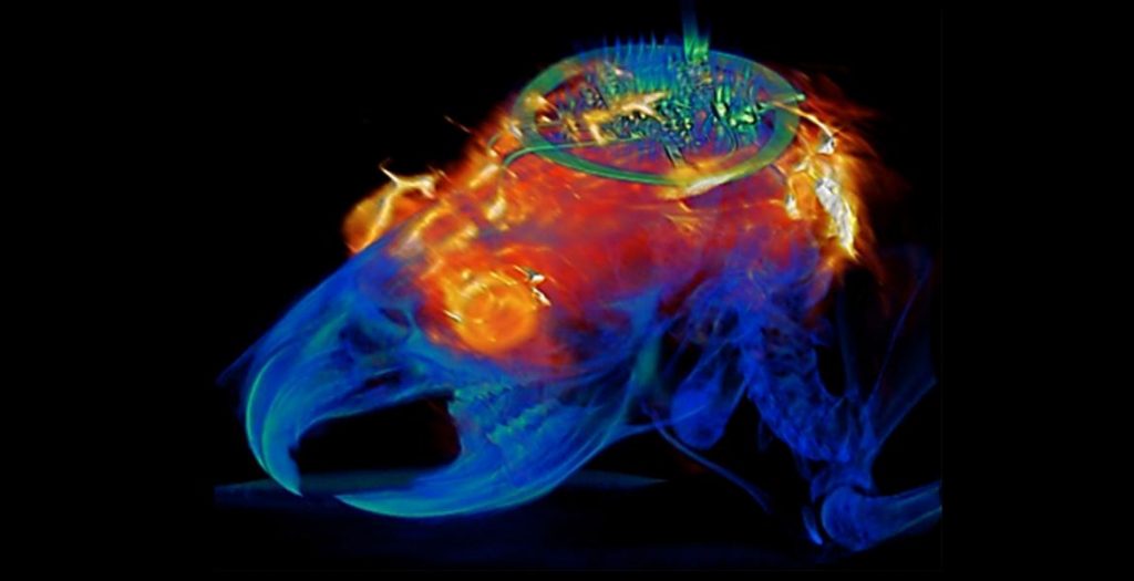
This image of a combined MRI (magnetic resonance image) and CT (computer tomography) scan bookends, more or less, the picture of the device which headed this piece,
Combined image analysis with MRI and CT results superimposed on a 3D rendering of the animal implanted with the programmable bilateral multi µ-ILED device. Courtesy: University of Arizona
Here’s a link to and a citation for the paper,
Fully implantable optoelectronic systems for battery-free, multimodal operation in neuroscience research by Philipp Gutruf, Vaishnavi Krishnamurthi, Abraham Vázquez-Guardado, Zhaoqian Xie, Anthony Banks, Chun-Ju Su, Yeshou Xu, Chad R. Haney, Emily A. Waters, Irawati Kandela, Siddharth R. Krishnan, Tyler Ray, John P. Leshock, Yonggang Huang, Debashis Chanda, & John A. Rogers. Nature Electronics volume 1, pages652–660 (2018) DOI: https://doi.org/10.1038/s41928-018-0175-0 Published 13 December 2018