My personal theme for this last year (2023) and for the coming year was and is: catching up. On the plus side, my 2023 backlog (roughly six months) to be published was whittled down considerably. On the minus side, I start 2024 with a backlog of two to three months.
2023 on this blog had a lot in common with 2022 (see my December 31, 2022 posting), which may be due to what’s going on in the world of emerging science and technology or to my personal interests or possibly a bit of both. On to 2023 and a further blurring of boundaries:
Energy, computing and the environment
The argument against paper is that it uses up resources, it’s polluting, it’s affecting the environment, etc. Somehow the part where electricity which underpins so much of our ‘smart’ society does the same thing is left out of the discussion.
Neuromorphic (brainlike) computing and lower energy
Before launching into the stories about lowering energy usage, here’s an October 16, 2023 posting “The cost of building ChatGPT” that gives you some idea of the consequences of our insatiable desire for more computing and more ‘smart’ devices,
…
In its latest environmental report, Microsoft disclosed that its global water consumption spiked 34% from 2021 to 2022 (to nearly 1.7 billion gallons , or more than 2,500 Olympic-sized swimming pools), a sharp increase compared to previous years that outside researchers tie to its AI research. [emphases mine]
“It’s fair to say the majority of the growth is due to AI,” including “its heavy investment in generative AI and partnership with OpenAI,” said Shaolei Ren, [emphasis mine] a researcher at the University of California, Riverside who has been trying to calculate the environmental impact of generative AI products such as ChatGPT.
…
Why it matters: Microsoft’s five WDM [West Des Moines in Iowa] data centers — the “epicenter for advancing AI” — represent more than $5 billion in investments in the last 15 years.
Yes, but: They consumed as much as 11.5 million gallons of water a month for cooling, or about 6% of WDM’s total usage during peak summer usage during the last two years, according to information from West Des Moines Water Works.
The focus is AI but it doesn’t take long to realize that all computing has energy and environmental costs. I have more about Ren’s work and about water shortages in the “The cost of building ChatGPT” posting.
This next posting would usually be included with my other art/sci postings but it touches on the issues. My October 13, 2023 posting about Toronto’s Art/Sci Salon events, in particular, there’s the Streaming Carbon Footprint event (just scroll down to the appropriate subhead). For the interested, I also found this 2022 paper “The Carbon Footprint of Streaming Media:; Problems, Calculations, Solutions” co-authored by one of the artist/researchers (Laura U. Marks, philosopher and scholar of new media and film at Simon Fraser University) who presented at the Toronto event.
I’m late to the party; Thomas Daigle posted a January 2, 2020 article about energy use and our appetite for computing and ‘smart’ devices for the Canadian Broadcasting Corporation’s online news,
For those of us binge-watching TV shows, installing new smartphone apps or sharing family photos on social media over the holidays, it may seem like an abstract predicament.
The gigabytes of data we’re using — although invisible — come at a significant cost to the environment. Some experts say it rivals that of the airline industry.
And as more smart devices rely on data to operate (think internet-connected refrigerators or self-driving cars), their electricity demands are set to skyrocket.
“We are using an immense amount of energy to drive this data revolution,” said Jane Kearns, an environment and technology expert at MaRS Discovery District, an innovation hub in Toronto.
“It has real implications for our climate.”
…
Some good news
Researchers are working on ways to lower the energy and environmental costs, here’s a sampling of 2023 posts with an emphasis on brainlike computing that attest to it,
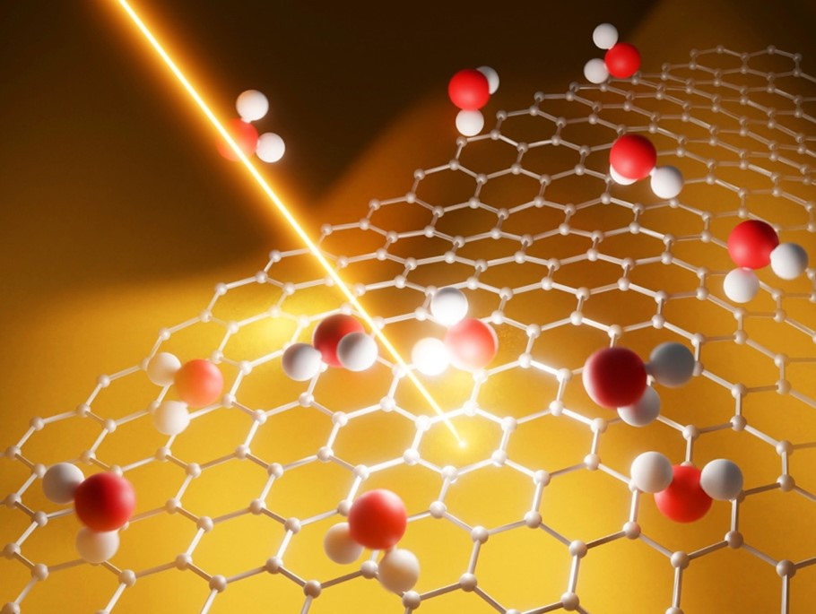
- January 30, 2023 posting: “Synaptic transistors for brainlike computers based on (more environmentally friendly) graphene“
- January 31, 2023 posting, “New chip for neuromorphic computing runs at a fraction of the energy of today’s systems“
- June 15, 2023 posting “Combining silicon with metal oxide memristors to create powerful, low-energy intensive chips enabling AI in portable devices“
- July 26, 2023 posting (I was late, the news was from March 2023), “Memristors based on halide perovskite nanocrystals are more powerful and easier to manufacture“
- October 12, 2023 posting, “IBM’s neuromorphic chip, a prototype and more“
- October 17, 2023 posting, “100-fold increase in AI energy efficiency“
- November 24, 2023 posting, “NorthPole: a brain-inspired chip design for saving energy“
If there’s an industry that can make neuromorphic computing and energy savings sexy, it’s the automotive indusry,
On the energy front,
Most people are familiar with nuclear fission and some its attendant issues. There is an alternative nuclear energy, fusion, which is considered ‘green’ or greener anyway. General Fusion is a local (Vancouver area) company focused on developing fusion energy, alongside competitors from all over the planet.
Part of what makes fusion energy attractive is that salt water or sea water can be used in its production and, according to that December posting, there are other applications for salt water power,
More encouraging developments in environmental science
Again, this is a selection. You’ll find a number of nano cellulose research projects and a couple of seaweed projects (seaweed research seems to be of increasing interest).
- March 6, 2023, “Seaweed battery“
- March 13, 2023 posting, “Cellulose nanofibers as an alternative material for petroleum-based plastics?“
- March 16, 2023 posting, “Plant fibers (nanocellulose) for more sustainable devices“
- June 8, 2023 posting, “Fairy-like robot powered by wind and light“
- June 20, 2023 posting, “Enabling a transparent wood battery that stores heat and regulates indoor temperature with lemons and coconuts“
- June 27, 2023 posting, “Biobattery with a 100-year shelf life“
- July 6, 2023 posting, “Greener cellulose-based products“
- July 26, 2023 posting, “Biodegradable electronics: a seaweed biosensor“
- July 25, 2023 posting, “A structural colour solution for energy-saving paint (thank the butterflies)“
- August 3, 2023 posting, “Remove 80 percent of dye pollutants from wastewater with wood nanocrystals“
- October 26, 2023 posting, “Using insect corpses to create biodegradable plastics“
- November 8, 2023 posting, “Nanocellulose and food waste, an Australian perspective“
- December 4, 2023, “The University of British Columbia and its November 28, 2023 Great UBC Bug Bake Off“
- December 5, 2023 posting, “AI for salmon recovery“
All by myself (neuromorphic engineering)
Neuromorphic computing is a subset of neuromorphic engineering and I stumbled across an article that outlines the similarities and differences. My ‘summary’ of the main points and a link to the original article can be found here,
Oops! I did it again. More AI panic
I included an overview of the various ‘recent’ panics (in my May 25, 2023 posting below) along with a few other posts about concerning developments but it’s not all doom and gloom..
- May 1, 2023 posting, “Canada, AI regulation, and the second reading of the Digital Charter Implementation Act, 2022 (Bill C-27)“
- May 25, 2023 posting, “Non-human authors (ChatGPT or others) of scientific and medical studies and the latest AI panic!!!“
- July 21, 2023 posting, “Lero (Science Foundation Ireland Research Centre for Software) researchers need to know (survey): Will artificial intelligence (AI) end civilization?“
- September 6, 2023 posting, “AI art threatens your humanity according to a study“
- October 19, 2023 posting, “AI ‘author’ steals another author’s identity“
- November 14, 2023 posting, “AI incites hiring of poets“
- November 28, 2023 posting, “An artificial, multisensory integrated neuron makes AI (artificial intelligence) smarter“
- December 7, 2023 posting, “AI-led corporate entities as a new species of legal subject“
Governments have realized that regulation might be a good idea. The European Union has a n AI act, the UK held an AI Safety Summit in November 2023, the US has been discussing AI regulation with its various hearings, and there’s impending legislation in Canada (see professor and lawyer Michael Geist’s blog for more).
A long time coming, a nanomedicine comeuppance
Paolo Macchiarini is now infamous for his untested, dangerous approach to medicine. Like a lot of people, I was fooled too as you can see in my August 2, 2011 posting, “Body parts nano style,”
In early July 2011, there were reports of a new kind of transplant involving a body part made of a biocomposite. Andemariam Teklesenbet Beyene underwent a trachea transplant that required an artificial windpipe crafted by UK experts then flown to Sweden where Beyene’s stem cells were used to coat the windpipe before being transplanted into his body.
It is an extraordinary story not least because Beyene, a patient in a Swedish hospital planning to return to Eritrea after his PhD studies in Iceland, illustrates the international cooperation that made the transplant possible.
The scaffolding material for the artificial windpipe was developed by Professor Alex Seifalian at the University College London in a landmark piece of nanotechnology-enabled tissue engineering. …
Five years later I stumbled across problems with Macchiarini’s work as outlined in my April 19, 2016 posting, “Macchiarini controversy and synthetic trachea transplants (part 1 of 2)” and my other April 19, 2016 posting, “Macchiarini controversy and synthetic trachea transplants (part 2 of 2)“.
This year, Gretchen Vogel (whose work was featured in my 2016 posts) has written a June 21, 2023 update about the Macchiarini affair for Science magazine, Note: Links have been removed,
Surgeon Paolo Macchiarini, who was once hailed as a pioneer of stem cell medicine, was found guilty of gross assault against three of his patients today and sentenced to 2 years and 6 months in prison by an appeals court in Stockholm. The ruling comes a year after a Swedish district court found Macchiarini guilty of bodily harm in two of the cases and gave him a suspended sentence. After both the prosecution and Macchiarini appealed that ruling, the Svea Court of Appeal heard the case in April and May. Today’s ruling from the five-judge panel is largely a win for the prosecution—it had asked for a 5-year sentence whereas Macchiarini’s lawyer urged the appeals court to acquit him of all charges.
Macchiarini performed experimental surgeries on the three patients in 2011 and 2012 while working at the renowned Karolinska Institute. He implanted synthetic windpipes seeded with stem cells from the patients’ own bone marrow, with the hope the cells would multiply over time and provide an enduring replacement. All three patients died when the implants failed. One patient died suddenly when the implant caused massive bleeding just 4 months after it was implanted; the two others survived for 2.5 and nearly 5 years, respectively, but suffered painful and debilitating complications before their deaths.
In the ruling released today, the appeals judges disagreed with the district court’s decision that the first two patients were treated under “emergency” conditions. Both patients could have survived for a significant length of time without the surgeries, they said. The third case was an “emergency,” the court ruled, but the treatment was still indefensible because by then Macchiarini was well aware of the problems with the technique. (One patient had already died and the other had suffered severe complications.)
…
A fictionalized tv series ( part of the Dr. Death anthology series) based on Macchiarini’s deceptions and a Dr. Death documentary are being broadcast/streamed in the US during January 2024. These come on the heels of a November 2023 Macchiarini documentary also broadcast/streamed on US television.
Dr. Death (anthology), based on the previews I’ve seen, is heavily US-centric, which is to be expected since Adam Ciralsky is involved in the production. Ciralsky wrote an exposé about Macchiarini for Vanity Fair published in 2016 (also featured in my 2016 postings). From a December 20, 2023 article by Julie Miller for Vanity Fair, Note: A link has been removed,
Seven years ago [2016], world-renowned surgeon Paolo Macchiarini was the subject of an ongoing Vanity Fair investigation. He had seduced award-winning NBC producer Benita Alexander while she was making a special about him, proposed, and promised her a wedding officiated by Pope Francis and attended by political A-listers. It was only after her designer wedding gown was made that Alexander learned Macchiarini was still married to his wife, and seemingly had no association with the famous names on their guest list.
Vanity Fair contributor Adam Ciralsky was in the midst of reporting the story for this magazine in the fall of 2015 when he turned to Dr. Ronald Schouten, a Harvard psychiatry professor. Ciralsky sought expert insight into the kind of fabulist who would invent and engage in such an audacious lie.
“I laid out the story to him, and he said, ‘Anybody who does this in their private life engages in the same conduct in their professional life,” recalls Ciralsky, in a phone call with Vanity Fair. “I think you ought to take a hard look at his CVs.”
That was the turning point in the story for Ciralsky, a former CIA lawyer who soon learned that Macchiarini was more dangerous as a surgeon than a suitor. …
Here’s a link to Ciralsky’s original article, which I described this way, from my April 19, 2016 posting (part 2 of the Macchiarini controversy),
For some bizarre frosting on this disturbing cake (see part 1 of the Macchiarini controversy and synthetic trachea transplants for the medical science aspects), a January 5, 2016 Vanity Fair article by Adam Ciralsky documents Macchiarini’s courtship of an NBC ([US] National Broadcasting Corporation) news producer who was preparing a documentary about him and his work.
[from Ciralsky’s article]
“Macchiarini, 57, is a magnet for superlatives. He is commonly referred to as “world-renowned” and a “super-surgeon.” He is credited with medical miracles, including the world’s first synthetic organ transplant, which involved fashioning a trachea, or windpipe, out of plastic and then coating it with a patient’s own stem cells. That feat, in 2011, appeared to solve two of medicine’s more intractable problems—organ rejection and the lack of donor organs—and brought with it major media exposure for Macchiarini and his employer, Stockholm’s Karolinska Institute, home of the Nobel Prize in Physiology or Medicine. Macchiarini was now planning another first: a synthetic-trachea transplant on a child, a two-year-old Korean-Canadian girl named Hannah Warren, who had spent her entire life in a Seoul hospital. … “
Other players in the Macchiarini story
Pierre Delaere, a trachea expert and professor of head and neck surgery at KU Leuven (a university in Belgium) was one of the first to draw attention to Macchiarini’s dangerous and unethical practices. To give you an idea of how difficult it was to get attention for this issue, there’s a September 1, 2017 article by John Rasko and Carl Power for the Guardian illustrating the issue. Here’s what they had to say about Delaere and other early critics of the work, Note: Links have been removed,
…
Delaere was one of the earliest and harshest critics of Macchiarini’s engineered airways. Reports of their success always seemed like “hot air” to him. He could see no real evidence that the windpipe scaffolds were becoming living, functioning airways – in which case, they were destined to fail. The only question was how long it would take – weeks, months or a few years.
Delaere’s damning criticisms appeared in major medical journals, including the Lancet, but weren’t taken seriously by Karolinska’s leadership. Nor did they impress the institute’s ethics council when Delaere lodged a formal complaint. [emphases mine]
Support for Macchiarini remained strong, even as his patients began to die. In part, this is because the field of windpipe repair is a niche area. Few people at Karolinska, especially among those in power, knew enough about it to appreciate Delaere’s claims. Also, in such a highly competitive environment, people are keen to show allegiance to their superiors and wary of criticising them. The official report into the matter dubbed this the “bandwagon effect”.
With Macchiarini’s exploits endorsed by management and breathlessly reported in the media, it was all too easy to jump on that bandwagon.
And difficult to jump off. In early 2014, four Karolinska doctors defied the reigning culture of silence [emphasis mine] by complaining about Macchiarini. In their view, he was grossly misrepresenting his results and the health of his patients. An independent investigator agreed. But the vice-chancellor of Karolinska Institute, Anders Hamsten, wasn’t bound by this judgement. He officially cleared Macchiarini of scientific misconduct, allowing merely that he’d sometimes acted “without due care”.
For their efforts, the whistleblowers were punished. [emphasis mine] When Macchiarini accused one of them, Karl-Henrik Grinnemo, of stealing his work in a grant application, Hamsten found him guilty. As Grinnemo recalls, it nearly destroyed his career: “I didn’t receive any new grants. No one wanted to collaborate with me. We were doing good research, but it didn’t matter … I thought I was going to lose my lab, my staff – everything.”
This went on for three years until, just recently [2017], Grinnemo was cleared of all wrongdoing.
…
It is fitting that Macchiarini’s career unravelled at the Karolinska Institute. As the home of the Nobel prize in physiology or medicine, one of its ambitions is to create scientific celebrities. Every year, it gives science a show-business makeover, picking out from the mass of medical researchers those individuals deserving of superstardom. The idea is that scientific progress is driven by the genius of a few.
It’s a problematic idea with unfortunate side effects. A genius is a revolutionary by definition, a risk-taker and a law-breaker. Wasn’t something of this idea behind the special treatment Karolinska gave Macchiarini? Surely, he got away with so much because he was considered an exception to the rules with more than a whiff of the Nobel about him. At any rate, some of his most powerful friends were themselves Nobel judges until, with his fall from grace, they fell too.
…
The September 1, 2017 article by Rasko and Power is worth the read if you have the interest and the time. And, Delaere has written up a comprehensive analysis, which includes basic information about tracheas and more, “The Biggest Lie in Medical History” 2020, PDF, 164 pp., Creative Commons Licence).
I also want to mention Leonid Schneider, science journalist and molecular cell biologist, whose work the Macchiarini scandal on his ‘For Better Science’ website was also featured in my 2016 pieces. Schneider’s site has a page titled, ‘Macchiarini’s trachea transplant patients: the full list‘ started in 2017 and which he continues to update with new information about the patients. The latest update was made on December 20, 2023.
Promising nanomedicine research but no promises and a caveat
Most of the research mentioned here is still in the laboratory. i don’t often come across work that has made its way to clinical trials since the focus of this blog is emerging science and technology,
- January 25, 2023 posting, “Lab-made cartilage gel for stiff, achy knees“
- May 9, 2023 posting, “Research on how the body will react to nanomedicines is inconsistent“
- June 14, 2023 posting, “Biohybrid device (a new type of neural implant) could restore limb function“
- July 14, 2023 posting, “Artificially-grown mini-brains (organoids)—without animal components— offer opportunities for neuroscience“
- *July 17, 2023 posting, “Unveiling the Neurotechnology Landscape: Scientific Advancements, Innovations and Major Trends—a UNESCO report“
- August 23, 2023 posting, “Nanoparticle drug delivery could reduce rejection rates for corneal transplants“
- December 1, 2023 posting, “Scientists at Indian Institute of Science (IISc) created hybrid nanoparticles made of gold and copper sulfide that can kill cancer cells“
- December 15, 2023 posting, “Reducing toxicity of Alzheimer’s proteins with graphene oxide“
*If you’re interested in the business of neurotechnology, the July 17, 2023 posting highlights a very good UNESCO report on the topic.
Funky music (sound and noise)
I have couple of stories about using sound for wound healing, bioinspiration for soundproofing applications, detecting seismic activity, more data sonification, etc.
- January 5, 2023 posting, “Sound absorbing wallpaper inspired by moth wings“
- January 23, 2023 posting, “Stifle the noise with seaweed“
- January 25, 2023 posting, “Making longer lasting bandages with sound and bubbles“
- February 13, 2023 posting, “It’s not just the sound, it’s the vibration too (a red-eyed treefrog calls for a mate)“
- May 4, 2023 posting, “A fish baying at the moon?“
- June 12, 2023 posting, “Music of the chemical elements“
- June 14, 2023 posting, “The sound of dirt“
- June 30, 2023 posting, “Sound waves for wearable patches that deliver drugs painlessly“
- August 18, 2023 posting, “Animals: Art, Science and Sound at the British Library in London, UK until August 28, 2023 and Digital Storytelling until October 15, 2023“
- December 12, 2023 posting, “Shape-changing speaker (aka acoustic swarms) for sound control“
- December 18, 2023 posting, “When the rocks sing “I got rhythm”“
- December 19,2023 posting, “The sounds of recent (December 2023) seismic activity in Iceland“
Same old, same old CRISPR
2023 was relatively quiet (no panics) where CRISPR developments are concerned but still quite active.
- January 12, 203 posting, “What is CRISPRnano?“
- March 8, 2023 posting, “Even a ‘good’ gene edit can go wrong“
- August 2, 2023 posting, “Gene-edited food: better tasting and/or allergen-free?“
- August 7, 2023 posting, “CRISPR-like system found in animals“
- December 22, 2023 posting, “Gene editing to identify and change parts of chicken DNA and limit the spread of bird flu virus“
Art/Sci: a pretty active year
I didn’t realize how active the year was art/sciwise including events and other projects until I reviewed this year’s postings. This is a selection from 2023 but there’s a lot more on the blog, just use the search term, “art/sci,” or “art/science,” or “sciart.”
While I often feature events and projects from these groups (e.g., June 2, 2023 posting, “Metacreation Lab’s greatest hits of Summer 2023“), it’s possible for me to miss a few. So, you can check out Toronto’s Art/Sci Salon’s website (strong focus on visual art) and Simon Fraser University’s Metacreation Lab for Creative Artificial Intelligence website (strong focus on music).
My selection of this year’s postings is more heavily weighted to the ‘writing’ end of things.
- February 10, 2023 posting, ““The Heart’s Knowledge: Science and Empathy in the Art of Dario Robleto” from Jan. 27 to July 9, 2023 at The Block Museum of Art (Northwestern University, Chicago, Illinois)“
- March 28,k 2023 posting, ““Living in a Dream,” part of Cambridge Festival (on display March 31 and April 1, 2023 in the UK)“
- April 4, 2023 posting, “Algorithmic haiku: Basho in the machine“
- April 5, 2023 posting, “Perimeter Institute (PI) presents: The Jazz of Physics with Stephon Alexander“
- May 15, 2023 posting, “‘Poetic meditation’ could enhance qualitative data analysis“
- June 9, 2023 posting, “Mary Shelley’s Frankenstein, the scientist who may have helped inspire the story, and a poetry/science project“
- June 22, 2023 posting, “Physics in James Joyce’s Ulysses and physics amongst the penguins“
- August 2, 2023 posting, “Every thing old is new again: using fairy tales to communicate science (energy research)“
- September 11, 2023 posting, “Leaning Out of Windows (LOoW): An Art and Physics Collaboration (2023 book) in Vancouver (Canada)“
Boundaries: life/nonlife
Last year I subtitled this section, ‘Aliens on earth: machinic biology and/or biological machinery?” Here’s this year’s selection,
- February 9, 2023 posting, “Living photovoltaics with carbon nanotubes (CNTs)?“
- March 17, 2023 posting, “Coelacanth (a living fish fossil) may provide clue to making artificial organs for transplantation“
- March 23 2023 posting, “Transforming bacterial cells into living computers“
- June 6 2023 posting, “In vitro biological neural networks (BNNs): review paper“
- June 30, 2023 posting, “International conference “Living Machines” dedicated to technology inspired by nature in Genoa, Italy (July 10 – 13, 2023)“
- July 13, 2023 posting, “Growing electrodes in your brain?“
- October 3, 2023 posting, “The art and science of architecture that is ‘living-like’“
- November 3, 2023 posting, “Nanoscale tattoos for individual cells“
- December 6, 2023 posting, “They glow under stress: soft, living materials made with algae“
Canada’s 2023 budget … military
2023 featured an unusual budget where military expenditures were going to be increased, something which could have implications for our science and technology research.
Then things changed as Murray Brewster’s November 21, 2023 article for the Canadian Broadcasting Corporation’s (CBC) news online website comments, Note: A link has been removed,
There was a revelatory moment on the weekend as Defence Minister Bill Blair attempted to bridge the gap between rhetoric and reality in the Liberal government’s spending plans for his department and the Canadian military.
Asked about an anticipated (and long overdue) update to the country’s defence policy (supposedly made urgent two years ago by Russia’s full-on invasion of Ukraine), Blair acknowledged that the reset is now being viewed through a fiscal lens.
“We said we’re going to bring forward a new defence policy update. We’ve been working through that,” Blair told CBC’s Rosemary Barton Live on Sunday.
“The current fiscal environment that the country faces itself does require (that) that defence policy update … recognize (the) fiscal challenges. And so it’ll be part of … our future budget processes.”
…
One policy goal of the existing defence plan, Strong, Secure and Engaged, was to require that the military be able to concurrently deliver “two sustained deployments of 500 [to] 1,500 personnel in two different theaters of operation, including one as a lead nation.”
In a footnote, the recent estimates said the Canadian military is “currently unable to conduct multiple operations concurrently per the requirements laid out in the 2017 Defence Policy. Readiness of CAF force elements has continued to decrease over the course of the last year, aggravated by decreasing number of personnel and issues with equipment and vehicles.”
Some analysts say they believe that even if the federal government hits its overall budget reduction targets, what has been taken away from defence — and what’s about to be taken away — won’t be coming back, the minister’s public assurances notwithstanding.
…
10 years: Graphene Flagship Project and Human Brain Project
“Graphene and Human Brain Project win biggest research award in history (& this is the 2000th post)” on January 28, 2013 was how I announced the results of what had been a a European Union (EU) competition that stretched out over several years and many stages as projects were evaluated and fell to the wayside or were allowed onto the next stage. The two finalists received €1B each to be paid out over ten years.
…
Future or not
As you can see, there was plenty of interesting stuff going on in 2023 but no watershed moments in the areas I follow. (Please do let me know in the Comments should you disagree with this or any other part of this posting.) Nanotechnology seems less and less an emerging science/technology in itself and more like a foundational element of our science and technology sectors. On that note, you may find my upcoming (in 2024) post about a report concerning the economic impact of its National Nanotechnology Initiative (NNI) from 2002 to 2022 of interest.
Following on the commercialization theme, I have noticed an increase of interest in commercializing brain and brainlike engineering technologies, as well as, more discussion about ethics.
Colonizing the brain?
UNESCO held events such as, this noted in my July 17, 2023 posting, “Unveiling the Neurotechnology Landscape: Scientific Advancements, Innovations and Major Trends—a UNESCO report” and this noted in my July 7, 2023 posting “Global dialogue on the ethics of neurotechnology on July 13, 2023 led by UNESCO.” An August 21, 2023 posting, “Ethical nanobiotechnology” adds to the discussion.
Meanwhile, Australia has been producing some very interesting mind/robot research, my June 13, 2023 posting, “Mind-controlled robots based on graphene: an Australian research story.” I have more of this kind of research (mind control or mind reading) from Australia to be published in early 2024. The Australians are not alone, there’s also this April 12, 2023 posting, “Mind-reading prosthetic limbs” from Germany.
My May 12, 2023 posting, “Virtual panel discussion: Canadian Strategies for Responsible Neurotechnology Innovation on May 16, 2023” shows Canada is entering the discussion. Unfortunately, the Canadian Science Policy Centre (CSPC), which held the event, has not posted a video online even though they have a youtube channel featuring other of their events.
As for neurmorphic engineering, China has produced a roadmap for its research in this area as noted in my March 20, 2023 posting, “A nontraditional artificial synaptic device and roadmap for Chinese research into neuromorphic devices.”
Quantum anybody?
I haven’t singled it out in this end-of-year posting but there is a great deal of interest in quantum computer both here in Canada and elsewhere. There is a 2023 report from the Council of Canadian Academies on the topic of quantum computing in Canada, which I hope to comment on soon.
Final words
I have a shout out for the Canadian Science Policy Centre, which celebrated its 15th anniversary in 2023. Congratulations!
For everyone, I wish peace on earth and all the best for you and yours in 2024!