Tag Archives: Jari Kinaret

10 years of the European Union’s roll of the dice: €1B or 1billion euros each for the Human Brain Project (HBP) and the Graphene Flagship

Graphene and Human Brain Project win biggest research award in history (& this is the 2000th post)” on January 28, 2013 was how I announced the results of what had been a a European Union (EU) competition that stretched out over several years and many stages as projects were evaluated and fell to the wayside or were allowed onto the next stage. The two finalists received €1B each to be paid out over ten years.

Human Brain Project (HBP)

A September 12, 2023 Human Brain Project (HBP) press release (also on EurekAlert) summarizes the ten year research effort and the achievements,

The EU-funded Human Brain Project (HBP) comes to an end in September and celebrates its successful conclusion today with a scientific symposium at Forschungszentrum Jülich (FZJ). The HBP was one of the first flagship projects and, with 155 cooperating institutions from 19 countries and a total budget of 607 million euros, one of the largest research projects in Europe. Forschungszentrum Jülich, with its world-leading brain research institute and the Jülich Supercomputing Centre, played an important role in the ten-year project.

“Understanding the complexity of the human brain and explaining its functionality are major challenges of brain research today”, says Astrid Lambrecht, Chair of the Board of Directors of Forschungszentrum Jülich. “The instruments of brain research have developed considerably in the last ten years. The Human Brain Project has been instrumental in driving this development – and not only gained new insights for brain research, but also provided important impulses for information technologies.”

HBP researchers have employed highly advanced methods from computing, neuroinformatics and artificial intelligence in a truly integrative approach to understanding the brain as a multi-level system. The project has contributed to a deeper understanding of the complex structure and function of the brain and enabled novel applications in medicine and technological advances.

Among the project’s highlight achievements are a three-dimensional, digital atlas of the human brain with unprecedented detail, personalised virtual models of patient brains with conditions like epilepsy and Parkinson’s, breakthroughs in the field of artificial intelligence, and an open digital research infrastructure – EBRAINS – that will remain an invaluable resource for the entire neuroscience community beyond the end of the HBP.

Researchers at the HBP have presented scientific results in over 3000 publications, as well as advanced medical and technical applications and over 160 freely accessible digital tools for neuroscience research.

“The Human Brain Project has a pioneering role for digital brain research with a unique interdisciplinary approach at the interface of neuroscience, computing and technology,” says Katrin Amunts, Director of the HBP and of the Institute for Neuroscience and Medicine at FZJ. “EBRAINS will continue to power this new way of investigating the brain and foster developments in brain medicine.”

“The impact of what you achieved in digital science goes beyond the neuroscientific community”, said Gustav Kalbe, CNECT, Acting Director of Digital Excellence and Science Infrastructures at the European Commission during the opening of the event. “The infrastructure that the Human Brain Project has established is already seen as a key building block to facilitate cooperation and research across geographical boundaries, but also across communities.”

Further information about the Human Brain Project as well as photos from research can be found here: https://fz-juelich.sciebo.de/s/hWJkNCC1Hi1PdQ5.

Results highlights and event photos in the online press release.

Results overviews:
– “Human Brain Project: Spotlights on major achievements” and “A closer Look on Scientific
Advances”

– “Human Brain Project: An extensive guide to the tools developed”

Examples of results from the Human Brain Project:
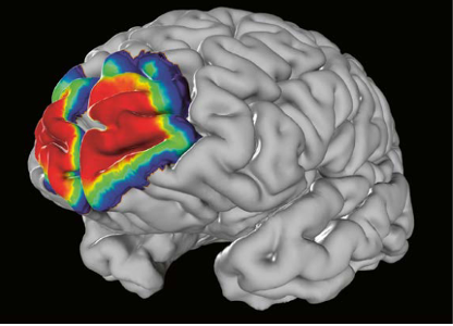
As the “Google Maps of the brain” [emphasis mine], the Human Brain Project makes the most comprehensive digital brain atlas to date available to all researchers worldwide. The atlas by Jülich researchers and collaborators combines high-resolution data of neurons, fibre connections, receptors and functional specialisations in the brain, and is designed as a constantly growing system.
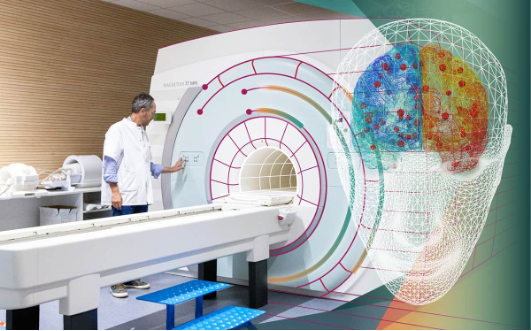
13 hospitals in France are currently testing the new “Virtual Epileptic Patient” – a platform developed at the University of Marseille [Aix-Marseille University?] in the Human Brain Project. It creates personalised simulation models of brain dynamics to provide surgeons with predictions for the success of different surgical treatment strategies. The approach was presented this year in the journals Science Translational Medicine and The Lancet Neurology.


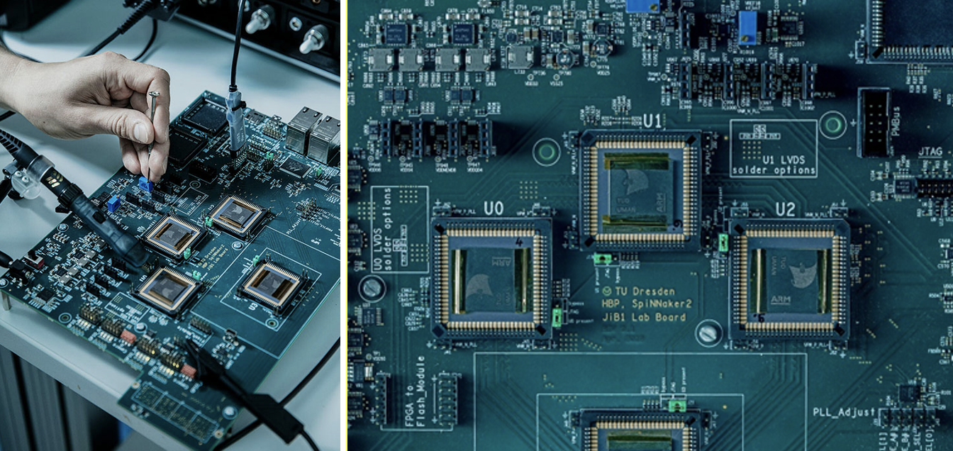
SpiNNaker2 is a “neuromorphic” [brainlike] computer developed by the University of Manchester and TU Dresden within the Human Brain Project. The company SpiNNcloud Systems in Dresden is commercialising the approach for AI applications. (Image: Sprind.org)

As an openly accessible digital infrastructure, EBRAINS offers scientists easy access to the best techniques for complex research questions.

[https://www.ebrains.eu/]

There was a Canadian connection at one time; Montréal Neuro at Canada’s McGill University was involved in developing a computational platform for neuroscience (CBRAIN) for HBP according to an announcement in my January 29, 2013 posting. However, there’s no mention of the EU project on the CBRAIN website nor is there mention of a Canadian partner on the EBRAINS website, which seemed the most likely successor to the CBRAIN portion of the HBP project originally mentioned in 2013.

I couldn’t resist “Google maps of the brain.”

In any event, the statement from Astrid Lambrecht offers an interesting contrast to that offered by the leader of the other project.

Graphene Flagship

In fact, the Graphene Flagship has been celebrating its 10th anniversary since last year; see my September 1, 2022 posting titled “Graphene Week (September 5 – 9, 2022) is a celebration of 10 years of the Graphene Flagship.”

The flagship’s lead institution, Chalmers University of Technology in Sweden, issued an August 28, 2023 press release by Lisa Gahnertz (also on the Graphene Flagship website but published September 4, 2023) touting its achievement with an ebullience I am more accustomed to seeing in US news releases,

Chalmers steers Europe’s major graphene venture to success

For the past decade, the Graphene Flagship, the EU’s largest ever research programme, has been coordinated from Chalmers with Jari Kinaret at the helm. As the project reaches the ten-year mark, expectations have been realised, a strong European research field on graphene has been established, and the journey will continue.

‘Have we delivered what we promised?’ asks Graphene Flagship Director Jari Kinaret from his office in the physics department at Chalmers, overlooking the skyline of central Gothenburg.

‘Yes, we have delivered more than anyone had a right to expect,’ [emphasis mine] he says. ‘In our analysis for the conclusion of the project, we read the documents that were written at the start. What we promised then were over a hundred specific things. Some of them were scientific and technological promises, and they have all been fulfilled. Others were for specific applications, and here 60–70 per cent of what was promised has been delivered. We have also delivered applications we did not promise from the start, but these are more difficult to quantify.’

The autumn of 2013 saw the launch of the massive ten-year Science, Technology and Innovation research programme on graphene and other related two-dimensional materials. Joint funding from the European Commission and EU Member States totalled a staggering €1,000 million. A decade later, it is clear that the large-scale initiative has succeeded in its endeavours. According to a report by the research institute WifOR, the Graphene Flagship will have created a total contribution to GDP of €3,800 million and 38,400 new jobs in the 27 EU countries between 2014 and 2030.

Exceeded expectations

‘Per euro invested and compared to other EU projects, the flagship has performed 13 times better than expected in terms of patent applications, and seven times better for scientific publications. We have 17 spin-off companies that have received over €130 million in private funding – people investing their own money is a real example of trust in the fact that the technology works,’ says Jari Kinaret.

He emphasises that the long time span has been crucial in developing the concepts of the various flagship projects.

‘When it comes to new projects, the ability to work on a long timescale is a must and is more important than a large budget. It takes a long time to build trust, both in one another within a team and in the technology on the part of investors, industry and the wider community. The size of the project has also been significant. There has been an ecosystem around the material, with many graphene manufacturers and other organisations involved. It builds robustness, which means you have the courage to invest in the material and develop it.’

From lab to application

In 2010, Andre Geim and Konstantin Novoselov of the University of Manchester won the Nobel Prize in Physics for their pioneering experiments isolating the ultra-light and ultra-thin material graphene. It was the first known 2D material and stunned the world with its ‘exceptional properties originating in the strange world of quantum physics’ according to the Nobel Foundation’s press release. Many potential applications were identified for this electrically conductive, heat-resistant and light-transmitting material. Jari Kinaret’s research team had been exploring the material since 2006, and when Kinaret learned of the European Commission’s call for a ten-year research programme, it prompted him to submit an application. The Graphene Flagship was initiated to ensure that Europe would maintain its leading position in graphene research and innovation, and its coordination and administration fell to Chalmers.

Is it a staggering thought that your initiative became the biggest EU research project of all time?

‘The fact that the three-minute presentation I gave at a meeting in Brussels has grown into an activity in 22 countries, with 170 organisations and 1,300 people involved … You can’t think about things like that because it can easily become overwhelming. Sometimes you just have to go for it,’ says Jari Kinaret.

One of the objectives of the Graphene Flagship was to take the hopes for this material and move them from lab to application. What has happened so far?

‘We are well on track with 100 products priced and on their way to the market. Many of them are business-to-business products that are not something we ordinary consumers are going to buy, but which may affect us indirectly.’

‘It’s important to remember that getting products to the application stage is a complex process. For a researcher, it may take ten working prototypes; for industry, ten million. Everything has to click into place, on a large scale. All components must work identically and in exactly the same way, and be compatible with existing production in manufacturing as you cannot rebuild an entire factory for a new material. In short, it requires reliability, reproducibility and manufacturability.’

Applications in a wide range of areas

Graphene’s extraordinary properties are being used to deliver the next generation of technologies in a wide range of fields, such as sensors for self-driving cars, advanced batteries, new water purification methods and sophisticated instruments for use in neuroscience. When asked if there are any applications that Jani Kinaret himself would like to highlight, he mentions, among other things, the applications that are underway in the automotive industry – such as sensors to detect obstacles for self-driving cars. Thanks to graphene, they will be so cost-effective to produce that it will be possible to make them available in more than just the most expensive car models.

He also highlights the aerospace industry, where a graphene material for removing ice from aircraft and helicopter wings is under development for the Airbus company. Another favourite, which he has followed from basic research to application, is the development of an air cleaner for Lufthansa passenger aircraft, based on a kind of ‘graphene foam’. Because graphene foam is very light, it can be heated extremely quickly. A pulse of electricity lasting one thousandth of a second is enough to raise the temperature to 300 degrees, thus killing micro-organisms and effectively cleaning the air in the aircraft.

He also mentions the Swedish company ABB, which has developed a graphene composite for circuit breakers in switchgear. These circuit breakers are used to protect the electricity network and must be safe to use. The graphene composite replaces the manual lubrication of the circuit breakers, resulting in significant cost savings.

‘We also see graphene being used in medical technology, but its application requires many years of testing and approval by various bodies. For example, graphene technology can more effectively map the brain before neurosurgery, as it provides a more detailed image. Another aspect of graphene is that it is soft and pliable. This means it can be used for electrodes that are implanted in the brain to treat tremors in Parkinson’s patients, without the electrodes causing scarring,’ says Jari Kinaret.

Coordinated by Chalmers

Jari Kinaret sees the fact that the EU chose Chalmers as the coordinating university as a favourable factor for the Graphene Flagship.

‘Hundreds of millions of SEK [Swedish Kroner] have gone into Chalmers research, but what has perhaps been more important is that we have become well-known and visible in certain areas. We also have the 2D-Tech competence centre and the SIO Grafen programme, both funded by Vinnova and coordinated by Chalmers and Chalmers industriteknik respectively. I think it is excellent that Chalmers was selected, as there could have been too much focus on the coordinating organisation if it had been more firmly established in graphene research at the outset.’

What challenges have been encountered during the project?

‘With so many stakeholders involved, we are not always in agreement. But that is a good thing. A management book I once read said that if two parties always agree, then one is redundant. At the start of the project, it was also interesting to see the major cultural differences we had in our communications and that different cultures read different things between the lines; it took time to realise that we should be brutally straightforward in our communications with one another.’

What has it been like to have the coordinating role that you have had?

‘Obviously, I’ve had to worry about things an ordinary physics professor doesn’t have to worry about, like a phone call at four in the morning after the Brexit vote or helping various parties with intellectual property rights. I have read more legal contracts than I thought I would ever have to read as a professor. As a researcher, your approach when you go into a role is narrow and deep, here it was rather all about breadth. I would have liked to have both, but there are only 26 hours in a day,’ jokes Jari Kinaret.

New phase for the project and EU jobs to come

A new assignment now awaits Jari Kinaret outside Chalmers as Chief Executive Officer of the EU initiative KDT JU (Key Digital Technologies Joint Undertaking, soon to become Chips JU), where industry and the public sector interact to drive the development of new electronic components and systems.

The Graphene Flagship may have reached its destination in its current form, but the work started is progressing in a form more akin to a flotilla. About a dozen projects will continue to live on under the auspices of the European Commission’s Horizon Europe programme. Chalmers is going to coordinate a smaller CSA project called GrapheneEU, where CSA stands for ‘Coordination and Support Action’. It will act as a cohesive force between the research and innovation projects that make up the next phase of the flagship, offering them a range of support and services, including communication, innovation and standardisation.

The Graphene Flagship is about to turn ten. If the project had been a ten-year-old child, what kind of child would it have been?

‘It would have been a very diverse organism. Different aspirations are beginning to emerge – perhaps it is adolescence that is approaching. In addition, within the project we have also studied other related 2D materials, and we found that there are 6,000 distinct materials of this type, of which only about 100 have been studied. So, it’s the younger siblings that are starting to arrive now.’

Facts about the Graphene Flagship:

The Graphene Flagship is the first European flagship for future and emerging technologies. It has been coordinated and administered from the Department of Physics at Chalmers, and as the project enters its next phase, GrapheneEU, coordination will continue to be carried out by staff currently working on the flagship led by Chalmers Professor Patrik Johansson.

The project has proved highly successful in developing graphene-based technology in Europe, resulting in 17 new companies, around 100 new products, nearly 500 patent applications and thousands of scientific papers. All in all, the project has exceeded the EU’s targets for utilisation from research projects by a factor of ten. According to the assessment of the EU research programme Horizon 2020, Chalmers’ coordination of the flagship has been identified as one of the key factors behind its success.

Graphene Week will be held at the Svenska Mässan in Gothenburg from 4 to 8 September 2023. Graphene Week is an international conference, which also marks the finale of the ten-year anniversary of the Graphene Flagship. The conference will be jointly led by academia and industry – Professor Patrik Johansson from Chalmers and Dr Anna Andersson from ABB – and is expected to attract over 400 researchers from Sweden, Europe and the rest of the world. The programme includes an exhibition, press conference and media activities, special sessions on innovation, diversity and ethics, and several technical sessions. The full programme is available here.

Read the press release on Graphene Week from 4 to 8 September and the overall results of the Graphene Flagship. …

Ten years and €1B each. Congratulations to the organizers on such massive undertakings. As for whether or not (and how they’ve been successful), I imagine time will tell.
Graphene Week (September 5 – 9, 2022) is a celebration of 10 years of the Graphene Flagship

Back in 2013 the European Union announced two huge targeted research investments €1B each for the Graphene Flagship and the Human Brain Project to be distributed over 10 years. (I have an overview of the Graphene Flagship’s high points from 2013-15 in my April 22, 2016 posting.)

Now at the ten year mark and its final days, the Graphene Flagship is celebrating 10 years with a Graphene Week (from an August 30, 2022 Graphene Flagship press release on EurekAlert),

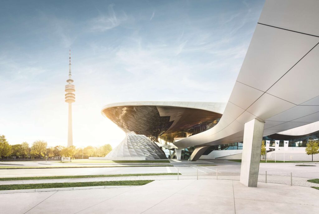
Graphene Week is a celebration of 10 years of the Graphene Flagship, a European Commission funded research project worth over €1 billion in funding. Held at BMW Welt — the exhibition space of one of the Graphene Flagship’s industrial partners based in Germany — the conference includes a comprehensive program of speakers, exhibitions, posters and a free pavilion.

The program includes a session on the European Chip Act, a notable point of debate for the continent. The act promises to mobilise more than €43 billion of both public and private investments to alleviate the global chip shortage. Graphene Week will demonstrate the potential of graphene-enabled alternatives to traditional semiconductors with the findings of the 2D-Experimental Pilot Line (2D-EPL).

The 2D-EPL is a €20 million project to integrate 2D materials into silicon wafers. The project has recently completed its first multi-project wafer (MPW) run, producing graphene integrated silicon wafers to academic and industrial customers.

During the conference Max Lemme of AMO GmbH in Germany and Sanna Arpiainen, of VTT Finland will discuss this subject along with the European Commission’s Thomas Skordas, Deputy Director General of DG CNECT and Bert De Colvenaer, Executive Director, KDT Joint Undertaking. Attendees can find the full program here.

The conference covers a large range of topics: from composites and medicine, to electronics and sensors. Beyond fundamental research, the talks by industry experts and European scientists will explore how graphene and related materials are disrupting critical European industries.

Graphene Week is co-chaired by Georg Duesberg from Bundeswehr University Munich and Elmar Bonaccurso, from Airbus Germany. In addition to Airbus, representatives from Lufthansa and other partners from the AEROGrAFT project will be in attendance, showcasing their graphene air filtration application for aircraft.   aircraft. 

Graphene Week will also host its Graphene Innovation Forum, a dedicated space for scientists to meet those in industry. Interactive panel discussions with industrial representatives will dive into future trends of graphene applications. The Innovation forum will feature speakers from both the Graphene Flagship’s large industrial partners including Medica, Lufthansa, Nokia and Airbus and smaller companies including Graphene Flagship spin-offs Emberion, BeDimensional and Qurv.

The Open Forum will collate some of the leading experts of the Graphene Flagship for a panel discussion on the success of graphene research and innovation where the audience is encouraged to ask questions. And the Diversity in Graphene initiative will offer a panel discussion focused on career development and professional use of social media.

The Graphene Flagship welcomes the public to explore the Graphene Pavilion in BMW Welt. The exhibition will showcase applications for graphene for cars, planes, phones and cities, together with product demos and videos. This pavilion will be free and open to the public from 9am on Friday 9 September to 6pm on Sunday 11 September.

“The Graphene Flagship is one of the largest ever EU projects, forming a network of 171 academic and industrial partners from 22 countries,” explained Jari Kinaret, Director of the Graphene Flagship. “In the 17th  edition, Graphene Week provides an opportunity to demonstrate the successes of the project and the ongoing legacy it will have on Europe’s industry. We look forward to welcoming our academic and industrial partners to join us in Munich for this celebration.”

More information on Graphene Week, access to the speaker line up and full scientific program can be found on the Graphene Flagship website. Registration provides access to all scientific sessions, sponsored sessions, access to the exhibition, conference material and more. To register click here.

This is the BMW Welt,

Looks like something out of a science fiction movie, eh?

You can find (Graphene Flagship spinoff companies), Emberion website here, BeDimensional website here, and Qurv Technologies website here.

Canada’s ‘Smart Cities’ will need new technology (5G wireless) and, maybe, graphene

I recently published [March 20, 2018] a piece on ‘smart cities’ both an art/science event in Toronto and a Canadian government initiative without mentioning the necessity of new technology to support all of the grand plans. On that note, it seems the Canadian federal government and two provincial (Québec and Ontario) governments are prepared to invest in one of the necessary ‘new’ technologies, 5G wireless. The Canadian Broadcasting Corporation’s (CBC) Shawn Benjamin reports about Canada’s 5G plans in suitably breathless (even in text only) tones of excitement in a March 19, 2018 article,

The federal, Ontario and Quebec governments say they will spend $200 million to help fund research into 5G wireless technology, the next-generation networks with download speeds 100 times faster than current ones can handle.

The so-called “5G corridor,” known as ENCQOR, will see tech companies such as Ericsson, Ciena Canada, Thales Canada, IBM and CGI kick in another $200 million to develop facilities to get the project up and running.

The idea is to set up a network of linked research facilities and laboratories that these companies — and as many as 1,000 more across Canada — will be able to use to test products and services that run on 5G networks.

Benjamin’s description of 5G is focused on what it will make possible in the future,

If you think things are moving too fast, buckle up, because a new 5G cellular network is just around the corner and it promises to transform our lives by connecting nearly everything to a new, much faster, reliable wireless network.

The first networks won’t be operational for at least a few years, but technology and telecom companies around the world are already planning to spend billions to make sure they aren’t left behind, says Lawrence Surtees, a communications analyst with the research firm IDC.

The new 5G is no tentative baby step toward the future. Rather, as Surtees puts it, “the move from 4G to 5G is a quantum leap.”

In a downtown Toronto soundstage, Alan Smithson recently demonstrated a few virtual reality and augmented reality projects that his company MetaVRse is working on.

The potential for VR and AR technology is endless, he said, in large part for its potential to help hurdle some of the walls we are already seeing with current networks.

Virtual Reality technology on the market today is continually increasing things like frame rates and screen resolutions in a constant quest to make their devices even more lifelike.

… They [current 4G networks] can’t handle the load. But 5G can do so easily, Smithson said, so much so that the current era of bulky augmented reality headsets could be replaced buy a pair of normal looking glasses.

In a 5G world, those internet-connected glasses will automatically recognize everyone you meet, and possibly be able to overlay their name in your field of vision, along with a link to their online profile. …

Benjamin also mentions ‘smart cities’,

In a University of Toronto laboratory, Professor Alberto Leon-Garcia researches connected vehicles and smart power grids. “My passion right now is enabling smart cities — making smart cities a reality — and that means having much more immediate and detailed sense of the environment,” he said.

Faster 5G networks will assist his projects in many ways, by giving planners more, instant data on things like traffic patterns, energy consumption, variou carbon footprints and much more.

Leon-Garcia points to a brightly lit map of Toronto [image embedded in Benjamin’s article] in his office, and explains that every dot of light represents a sensor transmitting real time data.

Currently, the network is hooked up to things like city buses, traffic cameras and the city-owned fleet of shared bicycles. He currently has thousands of data points feeding him info on his map, but in a 5G world, the network will support about a million sensors per square kilometre.

Very exciting but where is all this data going? What computers will be processing the information? Where are these sensors located? Benjamin does not venture into those waters nor does The Economist in a February 13, 2018 article about 5G, the Olympic Games in Pyeonchang, South Korea, but the magazine does note another barrier to 5G implementation,

“FASTER, higher, stronger,” goes the Olympic motto. So it is only appropriate that the next generation of wireless technology, “5G” for short, should get its first showcase at the Winter Olympics  under way in Pyeongchang, South Korea. Once fully developed, it is supposed to offer download speeds of at least 20 gigabits per second (4G manages about half that at best) and response times (“latency”) of below 1 millisecond. So the new networks will be able to transfer a high-resolution movie in two seconds and respond to requests in less than a hundredth of the time it takes to blink an eye. But 5G is not just about faster and swifter wireless connections.

The technology is meant to enable all sorts of new services. One such would offer virtual- or augmented-reality experiences. At the Olympics, for example, many contestants are being followed by 360-degree video cameras. At special venues sports fans can don virtual-reality goggles to put themselves right into the action. But 5G is also supposed to become the connective tissue for the internet of things, to link anything from smartphones to wireless sensors and industrial robots to self-driving cars. This will be made possible by a technique called “network slicing”, which allows operators quickly to create bespoke networks that give each set of devices exactly the connectivity they need.

Despite its versatility, it is not clear how quickly 5G will take off. The biggest brake will be economic. [emphasis mine] When the GSMA, an industry group, last year asked 750 telecoms bosses about the most salient impediment to delivering 5G, more than half cited the lack of a clear business case. People may want more bandwidth, but they are not willing to pay for it—an attitude even the lure of the fanciest virtual-reality applications may not change. …

That may not be the only brake, Dexter Johnson in a March 19, 2018 posting on his Nanoclast blog (on the IEEE [Institute of Electrical and Electronics Engineers] website), covers some of the others (Note: Links have been removed),

Graphene has been heralded as a “wonder material” for well over a decade now, and 5G has been marketed as the next big thing for at least the past five years. Analysts have suggested that 5G could be the golden ticket to virtual reality and artificial intelligence, and promised that graphene could improve technologies within electronics and optoelectronics.

But proponents of both graphene and 5G have also been accused of stirring up hype. There now seems to be a rising sense within industry circles that these glowing technological prospects will not come anytime soon.

At Mobile World Congress (MWC) in Barcelona last month [February 2018], some misgivings for these long promised technologies may have been put to rest, though, thanks in large part to each other.

In a meeting at MWC with Jari Kinaret, a professor at Chalmers University in Sweden and director of the Graphene Flagship, I took a guided tour around the Pavilion to see some of the technologies poised to have an impact on the development of 5G.

Being invited back to the MWC for three years is a pretty clear indication of how important graphene is to those who are trying to raise the fortunes of 5G. But just how important became more obvious to me in an interview with Frank Koppens, the leader of the quantum nano-optoelectronic group at Institute of Photonic Sciences (ICFO) just outside of Barcelona, last year.

He said: “5G cannot just scale. Some new technology is needed. And that’s why we have several companies in the Graphene Flagship that are putting a lot of pressure on us to address this issue.”

In a collaboration led by CNIT—a consortium of Italian universities and national laboratories focused on communication technologies—researchers from AMO GmbH, Ericsson, Nokia Bell Labs, and Imec have developed graphene-based photodetectors and modulators capable of receiving and transmitting optical data faster than ever before.

The aim of all this speed for transmitting data is to support the ultrafast data streams with extreme bandwidth that will be part of 5G. In fact, at another section during MWC, Ericsson was presenting the switching of a 100 Gigabits per second (Gbps) channel based on the technology.

“The fact that Ericsson is demonstrating another version of this technology demonstrates that from Ericsson’s point of view, this is no longer just research” said Kinaret.

It’s no mystery why the big mobile companies are jumping on this technology. Not only does it provide high-speed data transmission, but it also does it 10 times more efficiently than silicon or doped silicon devices, and will eventually do it more cheaply than those devices, according to Vito Sorianello, senior researcher at CNIT.

Interestingly, Ericsson is one of the tech companies mentioned with regard to Canada’s 5G project, ENCQOR and Sweden’s Chalmers University, as Dexter Johnson notes, is the lead institution for the Graphene Flagship.. One other fact to note, Canada’s resources include graphite mines with ‘premium’ flakes for producing graphene. Canada’s graphite mines are located (as far as I know) in only two Canadian provinces, Ontario and Québec, which also happen to be pitching money into ENCQOR. My March 21, 2018 posting describes the latest entry into the Canadian graphite mining stakes.

As for the questions I posed about processing power, etc. It seems the South Koreans have found answers of some kind but it’s hard to evaluate as I haven’t found any additional information about 5G and its implementation in South Korea. If anyone has answers, please feel free to leave them in the ‘comments’. Thank you.

Graphene Flagship experiences an upsurge in new partners

Almost doubling in size, from 78 partners to 140 partners, the European Union’s Graphene Flagship is doing nicely. From a June 23, 2014 news item on Nanowerk (Note: A link has been removed),

To coincide with Graphene Week 2014, the Graphene Flagship announced that today one of the largest-ever European research initiatives is doubling in size. 66 new partners are being invited to join the consortium following the results of a €9 million competitive call. [emphasis mine]

While most partners are universities and research institutes, the share of companies, mainly SMEs [small to medium enterprises], involved is increasing. This shows the growing interest of economic actors in graphene. The partnership now includes more than 140 organisations from 23 countries. [emphasis mine] It is fully set to take ‘wonder material’ graphene and related layered materials from academic laboratories to everyday use.

A June 23, 2014 Graphene Flagship news release (also on EurekAlert), which originated the news item, provides more detail about the partners and the call which attracted them,

The 66 new partners come from 19 countries, six of which are new to the consortium: Belarus, Bulgaria, the Czech Republic, Estonia, Hungary and Israel.

With its 16 new partners, Italy now has the highest number of partners in the Graphene Flagship alongside Germany (with 23 each), followed by Spain (18), UK (17) and France (13).

The incoming 66 partners will add new capabilities to the scientific and technological scope of the flagship. Over one third of new partners are companies, mainly SMEs, showing the growing interest of economic actors in graphene. In the initial consortium this ratio was 20%.

Big Interest in Joining the Initiative

The €9 million competitive call of the €54 million ramp-up phase (2014-2015) attracted a total of 218 proposals, representing 738 organisations from 37 countries. The proposals received were evaluated on the basis of their scientific and technological expertise, implementation and impact (further information on the call) and ranked by an international panel of leading experts, mostly eminent professors from all over the world. 21 proposals were selected for funding.

Prof. Jari Kinaret, Professor of Physics at the Chalmers University of Technology, Sweden, and Director of the Graphene Flagship, said: “The response was overwhelming, which is an indicator of the recognition for and trust in the flagship effort throughout Europe. Competition has been extremely tough. I am grateful for the engagement by the applicants and our nearly 60 independent expert reviewers who helped us through this process. I am impressed by the high quality of the proposals we received and looking forward to working with all the new partners to realise the goals of the Graphene Flagship.”

Europe in the Driving Seat

Graphene was made and tested in Europe, leading to the 2010 Nobel Prize in Physics for Andre Geim and Konstantin Novoselov from the University of Manchester.

With the €1 billion Graphene Flagship, Europe will be able to turn cutting-edge scientific research into marketable products. This major initiative places Europe in the driving seat for the global race to develop graphene technologies.

Prof. Andrea Ferrari, Director of the Cambridge Graphene Centre and Chair of the Executive Board of the Graphene Flagship commented today’s announcement on new partners: “This adds strength to our unprecedented effort to take graphene and related materials from the lab to the factory floor, so that the world-leading position of Europe in graphene science can be translated into technology, creating a new graphene-based industry, with benefits for Europe in terms of job creation and competitiveness”.

For anyone unfamiliar with the Graphene Flagship, the news release provides this backgrounder,

The Graphene Flagship @GrapheneCA represents a European investment of €1 billion over the next 10 years. It is part of the Future and Emerging Technologies (FET) Flagships @FETFlagships announced by the European Commission in January 2013 (press release). The goal of the FET Flagships programme is to encourage visionary research with the potential to deliver breakthroughs and major benefits for European society and industry. FET Flagships are highly ambitious initiatives involving close collaboration with national and regional funding agencies, industry and partners from outside the European Union.

Research in the next generation of technologies is key for Europe’s competitiveness. This is why €2.7 billion will be invested in Future and Emerging Technologies (FET) under the new research programme Horizon 2020 #H2020 (2014-2020). This represents a nearly threefold increase in budget compared to the previous research programme, FP7. FET actions are part of the Excellent science pillar of Horizon 2020.

You can find a full press kit for this announcement here, it includes,

I have long wondered how Sweden became the lead for the European Union effort. It seemed odd given that much of the initial work was done at the University of Manchester and the UK has not been shy about its ambition to lead the graphene effort internationally.

Graphene and Human Brain Project win biggest research award in history (& this is the 2000th post)

The European Commission has announced the two winners of its FET (Future and Emerging Technologies) Flagships Initiative in a Jan. 28, 2013 news release,

The winning Graphene and Human Brain initiatives are set to receive one billion euros each, to deliver 10 years of world-beating science at the crossroads of science and technology. Each initiative involves researchers from at least 15 EU Member States and nearly 200 research institutes.

“Graphene” will investigate and exploit the unique properties of a revolutionary carbon-based material. Graphene is an extraordinary combination of physical and chemical properties: it is the thinnest material, it conducts electricity much better than copper, it is 100-300 times stronger than steel and it has unique optical properties. The use of graphene was made possible by European scientists in 2004, and the substance is set to become the wonder material of the 21st century, as plastics were to the 20th century, including by replacing silicon in ICT products.

The “Human Brain Project” will create the world’s largest experimental facility for developing the most detailed model of the brain, for studying how the human brain works and ultimately to develop personalised treatment of neurological and related diseases. This research lays the scientific and technical foundations for medical progress that has the potential to will dramatically improve the quality of life for millions of Europeans.

The European Commission will support “Graphene” and the “Human Brain Project” as FET “flagships” over 10 years through its research and innovation funding programmes. Sustained funding for the full duration of the project will come from the EU’s research framework programmes, principally from the Horizon 2020 programme (2014-2020) which is currently negotiated in the European Parliament and Council.

European Commission Vice President Neelie Kroes said: “Europe’s position as a knowledge superpower depends on thinking the unthinkable and exploiting the best ideas. This multi-billion competition rewards home-grown scientific breakthroughs and shows that when we are ambitious we can develop the best research in Europe. To keep Europe competitive, to keep Europe as the home of scientific excellence, EU governments must agree an ambitious budget for the Horizon 2020 programme in the coming weeks.”

“Graphene” is led by Prof. Jari Kinaret, from Sweden’s Chalmers University. The Flagship involves over 100 research groups, with 136 principal investigators, including four Nobel laureates. “The Human Brain Project” involves scientists from 87 institutions and is led by Prof. Henry Markram of the École Polytechnique Fédérale de Lausanne.

As noted in my Jan. 24, 2013 posting about the new Cambridge Graphene Centre in the UK, while the Graphene flagship lead is from Sweden, the UK  has more educational institutions than any other country party to the flagship consortium.

Here are some funding details from the Jan. 28, 2013 news release,

Horizon 2020 is the new EU programme for research and innovation, presented by the Commission as part of its EU budget proposal for 2014 to 2020. In order to give a boost to research and innovation as a driver of growth and jobs, the Commission has proposed an ambitious budget of €80 billion over seven years, including the FET flagship programme itself.

The winners will receive up to €54 million from the European Commission’s ICT 2013 Work Programme. Further funding will come from subsequent EU research framework programmes, private partners including universities, Member States and industry.

1 billion Euros sounds like a lot of money but it’s being paid out over 10 years (100 million per year) and through many institutional layers at the European Commission and at the educational institutions themselves. One wonders how much of the money will go to research rather than administration.

2000th posting: My heartfelt thanks to everyone who has taken the time to read this blog and and to those who’ve taken the time to comment on the blog, on Twitter, or directly to me. Your interest has kept this blog going far longer than I believed it would.

Graphene 2012 and the Graphene flagship project

The Graphene Flagship project strikes again, this time at Graphene 2012, the second international conference on graphene. Here’s more about the conference, from the March 20, 2012 news item on Azonano,

Internationally renowned speakers will present the latest trends in the field and the global Graphene technology revolution. The Graphene 2012 program includes more than 100 speakers from all over the World, presentations from both research and industry.

Graphene 2012 [April 10 – 13, 2012 in Brussels, Belgium] is now an established European event, attracting global participants intent on sharing, exchanging and exploring new avenues of graphene-related scientific and commercial developments. Until now, the best, among many others, represented countries are United Kingdom, Germany, Spain, Belgium, France and United States.

I checked out the programme and found this front and centre,

Graphene Flagship Session

The consortium of the Graphene Flagship Pilot Action is working to establish the “Graphene Science and Technology Roadmap” which will be presented to the European Commission and Member States to demonstrate the need for securing long term funding, coordinated through a new Graphene Alliance. The Graphene Flagship Pilot Action will take advantage of the International conference Graphene 2012 in Brussels to co-organize a specific session in order to timely deliver to the European community the results of this Roadmap.

Tentative program

a. “Graphene Flagship: working together to combine scientific excellence and technological impacts”: Jari Kinaret
b. “The Graphene Science and Technology Roadmap”: Vladimir Falko and Andrea Ferrari
c. “Korean Graphene Research and Roadmap”: Byung Hee Hong
d . “Japanese Graphene Research and Roadmap”: Masataka Hasegawa
e. Round Table (tentative): Luigi Colombo, Gabriel Crean, Andrea Ferrari, Albert Fert, David Guedj, Francisco Guinea, Byung Hee Hong, Jari Kinaret, Klaus von Klitzing, and Ken Teo

I have commented previously on GRAPHENE-CA or the Graphene Flagship project, most recently in my Feb. 13, 2012 posting where I discuss the European Union’s Future and Emerging Technologies (FET) funding initiatives. The GRAPHENE-CA consortium is in competition for a 1B Euro research funding prize and they (particularly the UK) have been heroic in their promotional efforts, this new Graphene Alliance being yet another example.

Registration for the conference is here.

Brits go for the graphene gusto in Warsaw but where are the Swedes?

The Universities of Cambridge, Manchester, and Lancaster (all in the UK) have launched an exhibition extolling graphene in Warsaw (Poland). From the Nov. 25, 2011 news item on physorg.com,

The European programme for research into graphene, for which the Universities of Cambridge, Manchester and Lancaster are leading the technology roadmap, today unveiled an exhibition and new videos communicating the potential for the material that could revolutionise the electronics industries. [emphasis mine]

I’m a little confused as I thought the Swedish partner was either the leader or one of the lead partners.

I found this Nov. 24, 2011 news release from the University of Cambridge where the announcement was made,

An exhibition has been launched in Warsaw today highlighting the development and future of graphene, the ‘wonder substance’ set to change the face of electronics manufacturing, as part of the Graphene Flagship Pilot (GFP), aimed at developing the proposal for a 1 billion European programme conducting research and development on graphene, for which the Universities of Cambridge, Manchester and Lancaster are leading the technology roadmap.

The exhibition covers the development of the material, the present research and the vast potential for future applications. The GFP also released two videos aimed at introducing this extraordinary material to a wider audience, ranging from stakeholders and politicians to the general public. The videos also convey the mission and vision of the graphene initiative.

“Our mission is to take graphene and related layered materials from a state of raw potential to a point where they can revolutionise multiple industries – from flexible, wearable and transparent electronics to high performance computing and spintronics” says Professor Andrea Ferrari, Head of the Nanomaterials and Spectroscopy Group.

“This material will bring a new dimension to future technology – a faster, thinner, stronger, flexible, and broadband revolution. Our program will put Europe firmly at the heart of the process, with a manifold return on the investment of 1 billion Euros, both in terms of technological innovation and economic exploitation.”

Graphene, a single layer of carbon atoms, could prove to be the most versatile substance available to mankind. Stronger than diamond, yet lightweight and flexible, graphene enables electrons to flow much faster than silicon. It is also a transparent conductor, combining electrical and optical functionalities in an exceptional way.

This is connected to the European Union’s FET11 flagship projects initiative (described at more length in my June 13, 2011 graphene roundup posting) where six different research areas have been funded in preparation for a major funding round in late 2012 when two research projects will  be selected for a prize of 1B Euros each.

I find the communications strategy mildly confusing since the original project team listed Jari Kinaret of Chalmers University of Technology in Sweden (as highlighted in my Nov. 9, 2011 posting about funding for the Swedish effort with no mention of the other partners). The flagship group appears to be working both cooperatively and separately on the same project.

I did get a little curious as to the membership for this graphene research group (consortium) and found this,

1  CHALMERS UNIVERSITY OF TECHNOLOGY, Sweden

2  THE UNIVERSITY OF MANCHESTER,  United Kingdom

3  LANCASTER UNIVERSITY, United Kingdom

4  THE UNIVERSITY OF CAMBRIDGE, United Kingdom

5  AMO GMBH, Germany

6  CATALAN INSTITUTE OF NANOTECHNOLOGY, Spain

7  NATIONAL RESEARCH COUNCIL OF ITALY, Italy

8  NOKIA OYJ, Finland

9  EUROPEAN SCIENCE FOUNDATION, France

You can find more information about the Graphene Flagship Project here although they don’t appear to update the information very frequently.

Graphene, IBM’s first graphene-based integrated circuit, and the European Union’s pathfinder programme in information technologies

A flat layer of carbon atoms packed into a two-dimensional honeycomb arrangement, graphene is being touted as a miracle (it seems)  material which will enable new kinds of electronic products. Recently, there have been a number of news items and articles featuring graphene research.

Here’s my roundup of the latest and greatest graphene news. I’m starting with an application that is the closest to commercialization: IBM recently announced the creation of the first graphene-based integrated circuit. From the Bob Yirka article dated June 10, 2011 on physorg.com,

Taking a giant step forward in the creation and production of graphene based integrated circuits, IBM has announced in Science, the fabrication of a graphene based integrated circuit [IC] on a single chip. The demonstration chip, known as a radio frequency “mixer” is capable of producing frequencies up to 10 GHz, and demonstrates that it is possible to overcome the adhesion problems that have stymied researchers efforts in creating graphene based IC’s that can be used in analog applications such as cell phones or more likely military communications.

The graphene circuits were started by growing a two or three layer graphene film on a silicon surface which was then heated to 1400°C. The graphene IC was then fabricated by employing top gated, dual fingered graphene FET’s (field-effect transistors) which were then integrated with inductors. The active channels were made by spin-coating the wafer with a thin polymer and then applying a layer of hydrogen silsequioxane. The channels were then carved by e-beam lithography. Next, the excess graphene was removed with an oxygen plasma laser, and then the whole works was cleaned with acetone. The result is an integrated circuit that is less than 1mm2 in total size.

Meanwhile, there’s a graphene research project in contention for a major research prize in Europe. Worth 1B Euros, the European Union’s 2011 pathfinder programme (Future and Emerging Technologies [Fet11]) in information technology) will select two from six pilot actions currently under way to be awarded a Flagship Initiative prize.  From the Fet11 flagships project page,

FET Flagships are large-scale, science-driven and mission oriented initiatives that aim to achieve a visionary technological goal. The scale of ambition is over 10 years of coordinated effort, and a budget of up to one billion Euro for each Flagship. They initiatives are coordinated between national and EU programmes and present global dimensions to foster European leadership and excellence in frontier research.

To prepare the launch of the FET Flagships, 6 Pilot Actions are funded for a 12-month period starting in May 2011. In the second half of 2012 two of the Pilots will be selected and launched as full FET Flagship Initiatives in 2013.

Here’s the description of the Graphene Science and technology for ICT and beyond pilot action,

Graphene, a new substance from the world of atomic and molecular scale manipulation of matter, could be the wonder material of the 21st century. Discovering just how important this material will be for Information and Communication Technologies is the long term focus of the Flagship Initiative, simply called, GRAPHENE. This aims to explore revolutionary potentials, in terms of both conventional as well as radically new fields of Information and Communication Technologies applications.

Bringing together multiple disciplines and addressing research across a whole range of issues, from fundamental understandings of material properties to Graphene production, the Flagship will provide the platform for establishing European scientific and technological leadership in the application of Graphene to Information and Communication Technologies. The proposed research includes coverage of electronics, spintronics, photonics, plasmonics and mechanics, all based on Graphene.

[Project Team:]

Andrea Ferrari, Cambridge University, UK
Jari Kinaret, Chalmers University, Sweden
Vladimir Falko, Lancaster University, UK
Jani Kivioja, NOKIA, Finland [emphases mine]

Not so coincidentally (given one member of the team is associated with Nokia and another is associated with Cambridge University), the Nokia Research Centre jointly with Cambridge University issued a May 4, 2011 news release (I highlighted it in my May 6, 2011 posting [scroll down past the theatre project information]) about the Morph concept (a rigid, flexible, and stretchable phone/blood pressure cuff/calculator/and  other electronic devices in one product) which they have been publicizing for years now. The news release concerned itself with how graphene would enable the researchers to take the Morph from idea to actuality. The webpage for the Graphene Pilot Action is here.

There’s something breathtaking when there is no guarantee of success about the willingness to invest up to 1B Euros in a project that spans 10 years. We’ll have to wait until 2013 before learning whether the graphene project will be one of the two selected as Flagship Initiatives.

I must say the timing for the 2010 Nobel Prize for Physics which went to two scientists (Andre Geim and Konstantin Novoselov) for their groundbreaking work with graphene sems interesting (featured in my Oct. 7, 2010 posting) in light of this graphene activity.

The rest of these graphene items are about research that could lay the groundwork for future commercialization.

Friday, June 13, 2011 there was a news item about foaming graphene on Nanowerk (from the news item),

Hui-Ming Cheng and co-workers from the Chinese Academy of Sciences’ Institute of Metal Research at Shenyang have now devised a chemical vapor deposition (CVD) method for turning graphene sheets into porous three-dimensional ‘foams’ with extremely high conductivity (“Three-dimensional flexible and conductive interconnected graphene networks grown by chemical vapour deposition” [published in Nature Materials 10, 424–428 (2011) doi:10.1038/nmat3001 Published online 10 April 2011]). By permeating this foam with a siloxane-based polymer, the researchers have produced a composite that can be twisted, stretched and bent without harming its electrical or mechanical properties.

Here’s an image from the Nature Publishing Group (NPG) of both the vapour and the bendable, twistable, stretchable composite (downloaded from the news item on Nanowerk where you can find a larger version of the image),

A scanning electron microscopy image of the net-like structure of graphene foam (left), and a photograph of a highly conductive elastic conductor produced from the foam. (© 2011 NPG)

The ‘elastic’ conductor (image to the right) reminds me of the ‘paper’ phone which I wrote about May 8, 2011 and May 12, 2011. (It’s a project where teams from Queen’s University [in Ontario] and Arizona State University are working to create flexible screens that give you telephony, music playing and other capabilities  much like the Morph concept.)

Researchers in Singapore have developed a graphene quantum dot using a C60 (a buckminster fullerene). From the June 13, 2011 news item (Graphene: from spheres to perfect dots) on Nanowerk,

An electron trapped in a space of just a few nanometers across behaves very differently to one that is free. Structures that confine electrons in all three dimensions can produce some useful optical and electronic effects. Known as quantum dots, such structures are being widely investigated for use in new types of optical and electronics technologies, but because they are so small it is difficult to fabricate quantum dots reproducibly in terms of shape and size. Researchers from the National University of Singapore (NUS) and A*STAR have now developed a technique that enables graphene quantum dots of a known size to be created repeatedly and quickly (“Transforming C60 molecules into graphene quantum dots” [published in Nature Nanotechnology 6, 247–252 (2011) doi:10.1038/nnano.2011.30 Published online 20 March 2011]).

This final bit is about a nano PacMan that allows for more precise patterning from a June 13, 2011 article written by Michael Berger,

A widely discussed method for the patterning of graphene is the channelling of graphite by metal nanoparticles in oxidizing or reducing environments (see for instance: “Nanotechnology PacMan cuts straight graphene edges”).

“All previous studies of channelling behavior have been limited by the need to perform the experiment ex situ, i.e. comparing single ‘before’ and ‘after’ images,” Peter Bøggild, an associate professor at DTU [Danish Technical University] Nanotech, explains to Nanowerk. “In these and other ex situ experiments the dynamic behavior must be inferred from the length of channels and heating time after completion of the experiment, with the rate of formation of the channel assumed to be consistent over the course of the experiment.”

In new work, reported in the June 9, 2011 advance online edition of Nano Letters (“Discrete dynamics of nanoparticle channelling in suspended graphene” [published in Nano Letters, Article ASAP, DOI: 10.1021/nl200928k, Publication Date (Web): June 9, 2011]), Bøggild and his team report the nanoscale observation of this channelling process by silver nanoparticles in an oxygen atmosphere in-situ on suspended mono- and bilayer graphene in an environmental transmission electron microscope, enabling direct concurrent observation of the process, impossible in ex-situ experiments.

Personally, I love the youtube video I’ve included here largely because it features blobs (as many of these videos do) where they’ve added music and titles (many of these videos do not) so you can better appreciate the excitement,

From the article by Michael Berger,

As a result of watching this process occur live in a transmission electron microscope, the researchers say they have seen many details that were hidden before, and video really brings the “nano pacman” behavior to life …

There’s a reason why they’re so interested in cutting graphene,

“With a deeper understanding of the fine details we hope to one day use this nanoscale channelling behavior to directly cut desired patterns out of suspended graphene sheets, with a resolution and accuracy that isn’t achievable with any other technique,” says Bøggild. “A critical advantage here is that the graphene crystal structure guides the patterning, and in our case all of the cut edges of the graphene are ‘zigzag’ edges.”

So there you have it. IBM creates the first integrated graphene-based circuit, there’s the prospect of a huge cash prize for a 10-year project on graphene so they could produce the long awaited Morph concept and other graphene-based electronics products while a number of research teams around the world continue teasing out its secrets with graphene ‘foam’ projects, graphene quantum dots, and nano PacMen who cut graphene’s zigzag edges with precision.

ETA June 16, 2011: For those interested in the business end of things, i.e. market value of graphene-based products, Cameron Chai features a report, Graphene: Technologies, Applications, and Markets, in his June 16, 2011 news item on Azonano.