Monthly Archives: June 2015

Clinical trial for bionic eye (artificial retinal implant) shows encouraging results (safety and efficacy)

The Argus II artificial retina was first mentioned here in a Feb. 15, 2013 posting (scroll down about 50% of the way) when it received US Food and Drug Administration (FDA) commercial approval. In retrospect that seems puzzling since the results of a three-year clinical trial have just been reported in a June 23, 2015 news item on ScienceDaily (Note: There was one piece of information about the approval which didn’t make its way into the information disseminated in 2013),

The three-year clinical trial results of the retinal implant popularly known as the “bionic eye,” have proven the long-term efficacy, safety and reliability of the device that restores vision in those blinded by a rare, degenerative eye disease. The findings show that the Argus II significantly improves visual function and quality of life for people blinded by retinitis pigmentosa. They are being published online in Ophthalmology, the journal of the American Academy of Ophthalmology.

A June 23, 2015 American Academy of Ophthalmology news release (also on EurekAlert), which originated the news item, describes the condition the Argus II is designed for and that crucial bit of FDA information,

Retinitis pigmentosa is an incurable disease that affects about 1 in 4,000 Americans and causes slow vision loss that eventually leads to blindness.[1] The Argus II system was designed to help provide patients who have lost their sight due to the disease with some useful vision. Through the device, patients with retinitis pigmentosa are able to see patterns of light that the brain learns to interpret as an image. The system uses a miniature video camera stored in the patient’s glasses to send visual information to a small computerized video processing unit which can be stored in a pocket. This computer turns the image to electronic signals that are sent wirelessly to an electronic device implanted on the retina, the layer of light-sensing cells lining the back of the eye.

The Argus II received Food and Drug Administration (FDA) approval as a Humanitarian Use Device (HUD) in 2013, which is an approval specifically for devices intended to benefit small populations and/or rare conditions. [emphasis mine]

I don’t recall seeing “Humanitarian Use Device (HUD)” in the 2013 materials which focused on the FDA’s commercial use approval. I gather from this experience that commercial use doesn’t necessarily mean they’ve finished with clinical trials and are ready to start selling the product. In any event, I will try to take a closer look at the actual approvals the next time, assuming I can make sense of the language.

After all the talk about it, here’s what the device looks like,
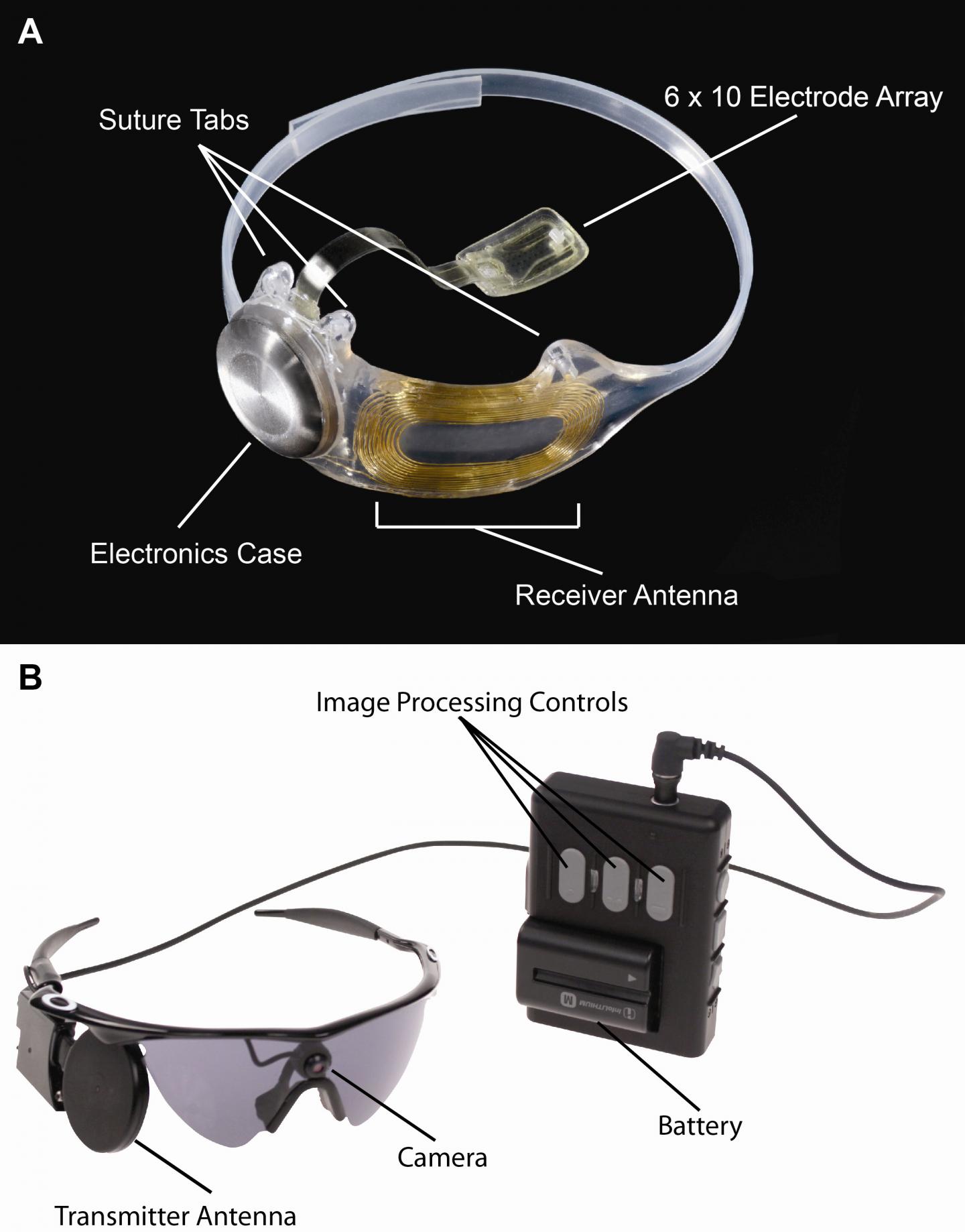
 Caption: Figure A, The implanted portions of the Argus II System. Figure B, The external components of the Argus II System. Images in real time are captured by camera mounted on the glasses. The video processing unit down-samples and processes the image, converting it to stimulation patterns. Data and power are sent via radiofrequency link form the transmitter antenna on the glasses to the receiver antenna around the eye. A removable, rechargeable battery powers the system. Credit: Photo courtesy of Second Sight Medical Products, Inc.


Caption: Figure A, The implanted portions of the Argus II System. Figure B, The external components of the Argus II System. Images in real time are captured by camera mounted on the glasses. The video processing unit down-samples and processes the image, converting it to stimulation patterns. Data and power are sent via radiofrequency link form the transmitter antenna on the glasses to the receiver antenna around the eye. A removable, rechargeable battery powers the system.
Credit: Photo courtesy of Second Sight Medical Products, Inc.

The news release offers more details about the recently completed clinical trial,

To further evaluate the safety, reliability and benefit of the device, a clinical trial of 30 people, aged 28 to 77, was conducted in the United States and Europe. All of the study participants had little or no light perception in both eyes. The researchers conducted visual function tests using both a computer screen and real-world conditions, including finding and touching a door and identifying and following a line on the ground. A Functional Low-vision Observer Rated Assessment (FLORA) was also performed by independent visual rehabilitation experts at the request of the FDA to assess the impact of the Argus II system on the subjects’ everyday lives, including extensive interviews and tasks performed around the home.

The visual function results indicated that up to 89 percent of the subjects performed significantly better with the device. The FLORA found that among the subjects, 80 percent received benefit from the system when considering both functional vision and patient-reported quality of life, and no subjects were affected negatively.

After one year, two-thirds of the subjects had not experienced device- or surgery-related serious adverse events. After three years, there were no device failures. Throughout the three years, 11 subjects experienced serious adverse events, most of which occurred soon after implantation and were successfully treated. One of these treatments, however, was to remove the device due to recurring erosion after the suture tab on the device became damaged.

“This study shows that the Argus II system is a viable treatment option for people profoundly blind due to retinitis pigmentosa – one that can make a meaningful difference in their lives and provides a benefit that can last over time,” said Allen C. Ho, M.D., lead author of the study and director of the clinical retina research unit at Wills Eye Hospital. “I look forward to future studies with this technology which may make possible expansion of the intended use of the device, including treatment for other diseases and eye injuries.”

Here’s a link to a PDF of and a citation for the paper,

Long-Term Results from an Epiretinal Prosthesis to Restore Sight to the Blind by Allen C. Ho,Mark S. Humayun, Jessy D. Dorn, Lyndon da Cruz, Gislin Dagnelie,James Handa, Pierre-Olivier Barale, José-Alain Sahel, Paulo E. Stanga, Farhad Hafezi, Avinoam B. Safran, Joel Salzmann, Arturo Santos, David Birch, Rand Spencer, Artur V. Cideciyan, Eugene de Juan, Jacque L. Duncan, Dean Eliott, Amani Fawzi, Lisa C. Olmos de Koo, Gary C. Brown, Julia A. Haller, Carl D. Regillo, Lucian V. Del Priore, Aries Arditi, Duane R. Geruschat, Robert J. Greenberg. Opthamology, June 2015 http://dx.doi.org/10.1016/j.ophtha.2015.04.032

This paper is open access.
Job posting (post doc in tissue engineering [organ-on-a-chip]) for the Istituto Italiano di Technologia

Here’s the posting (deadline is July 19, 2015),

Istituto Italiano di Tecnologia (IIT), Genova, Italy (http://www.iit.it) is a private law Foundation, created with special Government Law no. 269 dated September 30th 2003 with the objective of promoting Italy’s technological development and higher education in science and technology. Research at IIT is carried out in highly innovative scientific fields with state-of-the-art technology.

A post-doc position to develop “Organs-on-Chips” is available in the Laboratory of Nanotechnology for Precision Medicine at IIT.

Candidates should have a PhD in Tissue Engineering or closely related fields and an excellent publication record and should be highly motivated to work in an interdisciplinary team.

The candidate will work on the development of microfluidic-based organs-on-chips.

These microchips will be used to recapitulate the microarchitecture and functions of living organs and pathological tissues such as cancer and will possibly form an accurate alternative to traditional animal testing and enable high-throughput screening of drugs and nanomedicines.

The candidate should have:

  • strong skills in tissue engineering as well as in molecular, cellular and in vivo tumor biology;
  • documented experience in primary cell culture and analysis;
  • excellent oral and written communication skills in English and the ability to work both independently and as part of a multidisciplinary team.

Interested applicants should contact directly Dr. Paolo Decuzzi ( paolo.decuzzi@iit.it) for any informal queries.

For a formal application  please send CV, list of publications with Impact Factor and names and email addresses of 2 referees to applications@iit.it

Please apply by July 19, 2015 quoting “Post doc position in Tissue Engineering” in the mail subject. [emphasis mine]

In order to comply with Italian law (art. 23 of Privacy Law of the Italian Legislative Decree n. 196/03), the candidate is kindly asked to give his/her consent to allow Istituto Italiano di Tecnologia to process his/her personal data.

We inform you that the information you provide will be solely used for the purpose of evaluating and selecting candidates in order to meet the requirements of Istituto Italiano di Tecnologia.

Your data will be processed by Istituto Italiano di Tecnologia, with its headquarters in Genoa, Via Morego 30, acting as the Data Holder, using computer and paper-based means, observing the rules on the protection of personal data, including those relating to the security of data, and they will not be communicated to thirds.

Please also note that, pursuant to art.7 of Legislative Decree 196/2003, you may exercise your rights at any time as a party concerned by contacting the Data Holder.

Istituto Italiano di Tecnologia is an Equal Opportunity Employer that actively seeks diversity in the workforce.

Don’t forget when preparing your application, should you be living on the West Coast of Canada or the US (not sure about Mexico as its coast veers east somewhat), Italy is +9 hours . This means you’d best get your application submitted by 3 pm PST on July 19, 2015.

Herbicide nanometric sensor could help diagnose multiple sclerosis

This research into nanometric sensors and multiple sclerosis comes from Brazil. According to a June 23, 2015 news item on Nanowerk (Note: A link has been removed),

The early diagnosis of certain types of cancer, as well as nervous system diseases such as multiple sclerosis and neuromyelitis optica, may soon be facilitated by the use of a nanosensor capable of identifying biomarkers of these pathological conditions (“A Nanobiosensor Based on 4-Hydroxyphenylpyruvate Dioxygenase Enzyme for Mesotrione Detection”).

The nanobiosensor was developed at the Federal University of São Carlos (UFSCar), Sorocaba, in partnership with the São Paulo Federal Institute of Education, Science & Technology (IFSP), Itapetininga, São Paulo State, Brazil. It was originally designed to detect herbicides, heavy metals and other pollutants.

A June 23, 2015 Fundação de Amparo à Pesquisa do Estado de São Paulo news release on EurekAlert, which originated the news item, describes the sensor as it was originally used and explains its new function as a diagnostic tool for multiple sclerosis and other diseases,

“It’s a highly sensitive device, which we developed in collaboration with Alberto Luís Dario Moreau, a professor at IFSP. “We were able to increase sensitivity dramatically by going down to the nanometric scale,” said physicist Fábio de Lima Leite, a professor at UFSCar and the coordinator of the research group.

The nanobiosensor consists of a silicon nitride (Si3N4) or silicon (Si) nanoprobe with a molecular-scale elastic constant and a nanotip coupled to an enzyme, protein or other molecule.

When this molecule touches a target of interest, such as an antibody or antigen, the probe bends as the two molecules adhere. The deflection is detected and measured by the device, enabling scientists to identify the target.

“We started by detecting herbicides and heavy metals. Now we’re testing the device for use in detecting target molecules typical of nervous system diseases, in partnership with colleagues at leading centers of research on demyelinating diseases of the central nervous system”

The migration from herbicide detection to antibody detection was motivated mainly by the difficulty of diagnosing demyelinating diseases, cancer and other chronic diseases before they have advanced beyond an initial stage.

The criteria for establishing a diagnosis of multiple sclerosis or neuromyelitis optica are clinical (supplemented by MRI scans), and patients do not always present with a characteristic clinical picture. More precise diagnosis entails ruling out several other diseases.

The development of nanodevices will be of assistance in identifying these diseases and reducing the chances of false diagnosis.

The procedure can be as simple as placing a drop of the patient’s cerebrospinal fluid on a glass slide and observing its interaction with the nanobiosensor.

“If the interaction is low, we’ll be able to rule out multiple sclerosis with great confidence,” Leite said. “High interaction will indicate that the person is very likely to have the disease.” In this case, further testing would be required to exclude the possibility of a false positive.

“Different nervous system diseases have highly similar symptoms. Multiple sclerosis and neuromyelitis optica are just two examples. Even specialists experience difficulties or take a long time to diagnose them. Our technique would provide a differential diagnostic tool,” Leite said.

The next step for the group is to research biomarkers for these diseases that have not been completely mapped, including antibodies and antigens, among others. The group has begun tests for the detection of head and neck cancer.

Here’s a link to and a citation for the paper,

A Nanobiosensor Based on 4-Hydroxyphenylpyruvate Dioxygenase Enzyme for Mesotrione Detection by P. Soto Garcia, A.L.D Moreau, J.C. Magalhaes Ierich,  A.C Araujo Vig, A.M. Higa, G.S. Oliveira, F. Camargo Abdalla, M. Hausen, & F.L. Leite. Sensors Journal, IEEE  (Volume:15 ,  Issue: 4) pp. 2106 – 2113 Date of Publication: 20 November 2014 Date of Current Version: 27 January 2015 Issue Date: April 2015  DOI 10.1109/JSEN.2014.2371773

This paper is behind a paywall.

Knight Therapeutics, a Canadian pharmaceutical company, enters agreement with Russia’s (?) Pro Bono Bio, a nanotechnology product company

The June 27, 2015 news item on Nanotechnology Now includes two pieces of business news (I am more interested in the second),

Knight Therapeutics Inc. (TSX:GUD) (“Knight” or the “Company”), a leading Canadian specialty pharmaceutical company, announced today that it has (1) extended a secured loan of US$15 million to Pro Bono Bio PLC (“Pro Bono Bio”), the world’s leading healthcare nanotechnology company, and (2) entered into an exclusive distribution agreement with Pro Bono Bio to commercialize its wide range of nanotechnology products, medical devices and drug delivery technologies in select territories.

A June 26, 2015 Knight Pharmaceuticals news release, which originated the news item, provides a few more details about the loan and the license agreement,

The secured loan of US$15 million, which matures on June 25, 2018, will bear interest at 12% per annum plus other additional consideration. The interest rate will decrease to 10% if Pro Bono Bio meets certain equity-fundraising targets. The loan is secured by a charge over the assets of Pro Bono Bio and its affiliates which includes but is not limited to Flexiseq™, an innovative topical pain product that has sales of more than 3 million units since its U.K. launch last year.

As part of the license agreement, Knight obtained the exclusive Quebec and Israeli distribution rights to Pro Bono Bio’s innovative Flexiseq™ range of pain relief products and its promising SEQuaderma™ derma-cosmetic range of products, both of which are expected to launch in Quebec within the next 12 months. In addition, Knight obtained the exclusive Canadian and Israeli rights to two earlier stage product groups: blood factor products for the treatment of Hemophiliacs, and diagnostic devices designed for the automated detection of peripheral arterial disease. [emphasis mine]

John Mayo, Chairman and CEO of Pro Bono Bio, said, “We worked night and day to find a good distribution and strategic partner to help our North American team launch our existing products and drive growth. We welcome the good Knight on our quest to deliver to Canadian and American consumers’ best-in-class, drug-free nanotechnology products that are safe, effective and of the highest quality: truly the holy grail!”

“When you donate to charity, you always receive back more than you give. I hope this truism also holds true for this Pro Bono world!” said Jonathan Ross Goodman, President and CEO of Knight. “We look forward to the late 2015 launch of Flexiseq™ and SEQuaderma™ in La Belle Province.”

The news release also provides a description of the drugs and the companies, along with a disclaimer,

About Flexiseq™

Flexiseq™ is a topically applied drug-free gel which is clinically proven to safely relieve the pain and improve the joint stiffness associated with osteoarthritis (OA). Flexiseq™ is unique – it lubricates your joints to address joint damage. Pain is relieved and joint function improved because it lubricates away the friction and associated wear and tear on a user’s joints.

About SEQuaderma™

SEQuaderma™ Dermatology Products are a unique range of active dermatology solutions specifically designed to address the symptoms and, in some cases, the causes of the targeted conditions, leading to reduced recurrence. SEQuaderma™ Dermatology Products are suitable for long term use and can be used on their own or in between drug treatments to reduce exposure to adverse events; they will not compromise any other medication and are suitable for those with multiple conditions.

About Pro Bono Bio PLC

Pro Bono Bio PLC is the world’s leading healthcare nanotechnology company offering health and lifestyle products, headquartered in London with presence in Europe, Africa and Asia and due to launch in North America. [emphasis mine]

About Knight Therapeutics Inc.

Knight Therapeutics Inc., headquartered in Montreal, Canada, is a specialty pharmaceutical company focused on acquiring or in-licensing innovative pharmaceutical products for the Canadian and select international markets. Knight’s shares trade on TSX under the symbol GUD. For more information about Knight Therapeutics Inc., please visit the Company’s web site at www.gud-knight.com or www.sedar.com.

Forward-Looking Statement [disclaimer]

This document contains forward-looking statements for the Company and its subsidiaries. These forward looking statements, by their nature, necessarily involve risks and uncertainties that could cause actual results to differ materially from those contemplated by the forward-looking statements. The Company considers the assumptions on which these forward-looking statements are based to be reasonable at the time they were prepared, but cautions the reader that these assumptions regarding future events, many of which are beyond the control of the Company and its subsidiaries, may ultimately prove to be incorrect. Factors and risks, which could cause actual results to differ materially from current expectations are discussed in the Company’s Annual Report and in the Company’s Annual Information Form for the year ended December 31, 2014. The Company disclaims any intention or obligation to update or revise any forward-looking statements whether as a result of new information or future events, except as required by law.

While Pro Bono Bio is headquartered in London (UK), the BloombergBusiness website lists the company as Russian,

Pro Bono Bio, an international pharmaceutical company, develops and commercializes new medicines in the Russian Federation. Its products include FLEXISEQ, a pain relieving gel containing absorbing nanostructures (Sequessomes) for the treatment of pain associated with osteoarthritis; EXOSEQ, which delivers Sequessomes to the upper dermal layers of the skin for the treatment of inflammatory conditions, such as eczema and seborrhoeic dermatitis; and ROSSOSEQ, which distributes Sequessome vesicles into lower dermal tissues in the skin to treat psoriasis and atopic eczema conditions. The company also develops blood products, CV diagnostics, anti-infectives, and biological drugs. Pro Bono Bio was …

Detailed Description

Moscow,

Russia

Founded in 2011

www.probonobio.com
Key Executives for Pro Bono Bio
Mr. John Mayo
Chief Executive Officer
Mr. Michael Earl
Chief Operating Officer
Compensation as of Fiscal Year 2014.

Pro Bono Bio Key Developments

Pro Bono Bio Appoints Jason Flowerday as CEO of North American Operations

Jun 26 15

Pro Bono Bio launched its North American operations with headquarters based in Toronto, Canada and secured USD 15 million in funding to accelerate the global launches of FLEXISEQ and SEQUADERMA as well as help fund its ambitious research and development programs that continue to place Pro Bono Bio at the forefront of nanotechnology healthcare development. Pro Bono Bio has recently appointed a North American CEO, Jason Flowerday, to build-out the North American operations and set its strategy for entering both the Canadian and US markets over the next three quarters.

Pro Bono Bio Launches its North American Operations
Jun 26 15

These are interesting developments for both Montréal (Québec) and Toronto (Ontario). As for whether or not Pro Bono Bio is Russian or British, I imagine the legal entity which is the company is Russian while the operations (headquarters as previously noted) are based in the UK.

Solar-powered sensors to power the Internet of Things?

As a June 23, 2015 news item on Nanowerk notes, the ‘nternet of things’, will need lots and lots of power,

The latest buzz in the information technology industry regards “the Internet of things” — the idea that vehicles, appliances, civil-engineering structures, manufacturing equipment, and even livestock would have their own embedded sensors that report information directly to networked servers, aiding with maintenance and the coordination of tasks.

Realizing that vision, however, will require extremely low-power sensors that can run for months without battery changes — or, even better, that can extract energy from the environment to recharge.

Last week, at the Symposia on VLSI Technology and Circuits, MIT [Massachusetts Institute of Technology] researchers presented a new power converter chip that can harvest more than 80 percent of the energy trickling into it, even at the extremely low power levels characteristic of tiny solar cells. [emphasis mine] Previous experimental ultralow-power converters had efficiencies of only 40 or 50 percent.

A June 22, 2015 MIT news release (also on EurekAlert), which originated the news item, describes some additional capabilities,

Moreover, the researchers’ chip achieves those efficiency improvements while assuming additional responsibilities. Where its predecessors could use a solar cell to either charge a battery or directly power a device, this new chip can do both, and it can power the device directly from the battery.

All of those operations also share a single inductor — the chip’s main electrical component — which saves on circuit board space but increases the circuit complexity even further. Nonetheless, the chip’s power consumption remains low.

“We still want to have battery-charging capability, and we still want to provide a regulated output voltage,” says Dina Reda El-Damak, an MIT graduate student in electrical engineering and computer science and first author on the new paper. “We need to regulate the input to extract the maximum power, and we really want to do all these tasks with inductor sharing and see which operational mode is the best. And we want to do it without compromising the performance, at very limited input power levels — 10 nanowatts to 1 microwatt — for the Internet of things.”

The prototype chip was manufactured through the Taiwan Semiconductor Manufacturing Company’s University Shuttle Program.

The MIT news release goes on to describe chip specifics,

The circuit’s chief function is to regulate the voltages between the solar cell, the battery, and the device the cell is powering. If the battery operates for too long at a voltage that’s either too high or too low, for instance, its chemical reactants break down, and it loses the ability to hold a charge.

To control the current flow across their chip, El-Damak and her advisor, Anantha Chandrakasan, the Joseph F. and Nancy P. Keithley Professor in Electrical Engineering, use an inductor, which is a wire wound into a coil. When a current passes through an inductor, it generates a magnetic field, which in turn resists any change in the current.

Throwing switches in the inductor’s path causes it to alternately charge and discharge, so that the current flowing through it continuously ramps up and then drops back down to zero. Keeping a lid on the current improves the circuit’s efficiency, since the rate at which it dissipates energy as heat is proportional to the square of the current.

Once the current drops to zero, however, the switches in the inductor’s path need to be thrown immediately; otherwise, current could begin to flow through the circuit in the wrong direction, which would drastically diminish its efficiency. The complication is that the rate at which the current rises and falls depends on the voltage generated by the solar cell, which is highly variable. So the timing of the switch throws has to vary, too.

Electric hourglass

To control the switches’ timing, El-Damak and Chandrakasan use an electrical component called a capacitor, which can store electrical charge. The higher the current, the more rapidly the capacitor fills. When it’s full, the circuit stops charging the inductor.

The rate at which the current drops off, however, depends on the output voltage, whose regulation is the very purpose of the chip. Since that voltage is fixed, the variation in timing has to come from variation in capacitance. El-Damak and Chandrakasan thus equip their chip with a bank of capacitors of different sizes. As the current drops, it charges a subset of those capacitors, whose selection is determined by the solar cell’s voltage. Once again, when the capacitor fills, the switches in the inductor’s path are flipped.

“In this technology space, there’s usually a trend to lower efficiency as the power gets lower, because there’s a fixed amount of energy that’s consumed by doing the work,” says Brett Miwa, who leads a power conversion development project as a fellow at the chip manufacturer Maxim Integrated. “If you’re only coming in with a small amount, it’s hard to get most of it out, because you lose more as a percentage. [El-Damak’s] design is unusually efficient for how low a power level she’s at.”

“One of the things that’s most notable about it is that it’s really a fairly complete system,” he adds. “It’s really kind of a full system-on-a chip for power management. And that makes it a little more complicated, a little bit larger, and a little bit more comprehensive than some of the other designs that might be reported in the literature. So for her to still achieve these high-performance specs in a much more sophisticated system is also noteworthy.”

I wonder how close they are to commercializing this chip (see below),

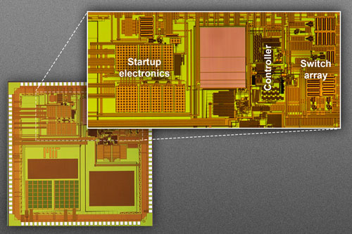
The MIT researchers' prototype for a chip measuring 3 millimeters by 3 millimeters. The magnified detail shows the chip's main control circuitry, including the startup electronics; the controller that determines whether to charge the battery, power a device, or both; and the array of switches that control current flow to an external inductor coil. This active area measures just 2.2 millimeters by 1.1 millimeters. (click on image to enlarge) Read more: Toward tiny, solar-powered sensors. Courtesy: MIT

The MIT researchers’ prototype for a chip measuring 3 millimeters by 3 millimeters. The magnified detail shows the chip’s main control circuitry, including the startup electronics; the controller that determines whether to charge the battery, power a device, or both; and the array of switches that control current flow to an external inductor coil. This active area measures just 2.2 millimeters by 1.1 millimeters. (click on image to enlarge)
Courtesy: MIT

Labeling 5nm gold nanoparticles with gold isotopes (soft core, hard shell)

There’s a lot of talk about using gold nanoparticles (and others) to deliver drugs to specific locations in the body but this research at Helmholtz Zentrum Muenchen (Munich, Germany) and the University of Marburg (Marburg, Germany) appears to be the first successful attempt at tracking how this potential delivery system might actually work. From a June 23, 2015 news item on Azonano,

Nanoparticles are the smallest particles capable of reaching virtually all parts of the body. Researchers use various approaches to test ways in which nanoparticles could be used in medicine – for instance, to deliver substances to a specific site in the body such as a tumor.

For this purpose, nanoparticles are generally coated with organic materials because their surface quality plays a key role in determining further targets in the body. If they have a water-repellent shell, nanoparticles are quickly identified by the body’s immune system and eliminated.

How gold particles wander through the body

The team of scientists headed by Dr. Wolfgang Kreyling, who is now an external scientific advisor at the Institute of Epidemiology II within the Helmholtz Zentrum Muenchen, and Prof. Wolfgang Parak from the University of Marburg, succeeded for the first time in tracking the chronological sequence of such particles in an animal model. To this end, they generated tiny 5 nm gold nanoparticles radioactively labeled with a gold isotope*. These were also covered with a polymer shell and tagged with a different radioactive isotope. According to the researchers, this was, technically speaking, a very demanding nanotechnological step.

A June 22, 2015 Helmholtz Zentrum Muenchen press release, which originated the news item, provides more detail,

After the subsequent intravenous injection of the particles, however, the team observed how the specially applied polymer shell disintegrated. “Surprisingly, the particulate gold accumulated mainly in the liver,” Dr. Kreyling recalls. “In contrast, the shell molecules reacted in a significantly different manner, distributing themselves throughout the body.” Further analyses conducted by the scientists explained the reason for this: so-called proteolytic enzymes** in certain liver cells appear to separate the particles from their shell. According to the researchers, this effect was hitherto unknown in vivo, since up to now the particle-conjugate had only been tested in cell cultures, where this effect had not been examined sufficiently thoroughly.

“Our results show that even nanoparticle-conjugates*** that appear highly stable can change their properties when deployed in the human body,” Dr. Kreyling notes, evaluating the results. “The study will thus have an influence on future medical applications as well as on the risk evaluation of nanoparticles in consumer products and in science and technology.”

* Isotopes are types of atoms which have different mass numbers but which represent the same element.

** Proteolytic enzymes split protein structures and are used, for example, to nourish or detoxify the body.

*** Conjugates are several types of molecules that are bound in one particle.

Here’s a link to and a citation for the paper,

In vivo integrity of polymer-coated gold nanoparticles by Wolfgang G. Kreyling, Abuelmagd M. Abdelmonem, Zulqurnain Ali, Frauke Alves, Marianne Geiser, Nadine Haberl, Raimo Hartmann, Stephanie Hirn, Dorleta Jimenez de Aberasturi, Karsten Kantner, Gülnaz Khadem-Saba, Jose-Maria Montenegro, Joanna Rejman, Teofilo Rojo, Idoia Ruiz de Larramendi, Roser Ufartes, Alexander Wenk, & Wolfgang J. Parak. Nature Nanotechnology (2015) doi:10.1038/nnano.2015.111 Published online 15 June 2015

This paper is behind a paywall.

Canadian science media at June 28, 2015 SpaceX Dragon CRS-7 cargo mission to the International Space Station

The short story is that Elizabeth Hand, Digital Engagement Specialist, at Vancouver’s (Canada) Science World was selected to be a correspondent at the Cape Canaveral (Florida) Space X launch on June 28, 2015. There’s more in her June 24, 2015 posting on the Vancouver Sun newspaper blog network (Note: Links and some formatting niceties have been removed),

I [am] on my way to Cape Canaveral Air Force Station in Florida to join a team of social media correspondents from all over the world as a representative of Science World British Columbia to view the June 28, 2015 SpaceX Dragon CRS-7 cargo mission to the International Space Station.

I  received the news that I had been offered an invite at my thirty-something birthday celebration dinner. It was the gift to end all birthday gifts—a once-in-a-lifetime space nerd adventure. Any rocket launch would have made me happy, but a launch from Cape Canaveral is a particularly special one. For me, in particular, because I grew up in Florida and I can remember standing outside in the school yard hoping to catch a glimpse of the space shuttles that moved the Americans to the stars in the 80’s and 90’s. I dreamed of going up with them.

I am excited to bring the curiosity and excitement of the kids in BC with me to the events. Kids of all ages are invited to send their questions about space and rockets to @scienceworldca and/or @bettyHand on both Instagram and Twitter with the hashtag #whyspacematters. You can participate from home or from Science World, where, from June 24-28, kids can dress up in space suits and, with the help of our science facilitators, can snap photos and share their ideas and questions with me and the experts at NASA and SpaceX.

It’s not clear to me if she will be blogging live as well as using the vehicles (Twitter, etc.) mentioned in her posting*. It might be worth checking both the Vancouver Sun (Community Blogs Network) and Science World (blog) to see if she will be offering more substantive descriptions than are possible on the social media vehicles she mentioned.

* ‘posing’ corrected to ‘posting’ at 1115 hours on June 26, 2015.

ETA June 29, 2015: The rocket exploded nine minutes after launch (Daniel Terdiman’s June 28, 2015 posting for Fast Company).

D-Wave passes 1000-qubit barrier

A local (Vancouver, Canada-based, quantum computing company, D-Wave is making quite a splash lately due to a technical breakthrough.  h/t’s Speaking up for Canadian Science for Business in Vancouver article and Nanotechnology Now for Harris & Harris Group press release and Economist article.

A June 22, 2015 article by Tyler Orton for Business in Vancouver describes D-Wave’s latest technical breakthrough,

“This updated processor will allow significantly more complex computational problems to be solved than ever before,” Jeremy Hilton, D-Wave’s vice-president of processor development, wrote in a June 22 [2015] blog entry.

Regular computers use two bits – ones and zeroes – to make calculations, while quantum computers rely on qubits.

Qubits possess a “superposition” that allow it to be one and zero at the same time, meaning it can calculate all possible values in a single operation.

But the algorithm for a full-scale quantum computer requires 8,000 qubits.

A June 23, 2015 Harris & Harris Group press release adds more information about the breakthrough,

Harris & Harris Group, Inc. (Nasdaq: TINY), an investor in transformative companies enabled by disruptive science, notes that its portfolio company, D-Wave Systems, Inc., announced that it has successfully fabricated 1,000 qubit processors that power its quantum computers.  D-Wave’s quantum computer runs a quantum annealing algorithm to find the lowest points, corresponding to optimal or near optimal solutions, in a virtual “energy landscape.”  Every additional qubit doubles the search space of the processor.  At 1,000 qubits, the new processor considers 21000 possibilities simultaneously, a search space which is substantially larger than the 2512 possibilities available to the company’s currently available 512 qubit D-Wave Two. In fact, the new search space contains far more possibilities than there are particles in the observable universe.

A June 22, 2015 D-Wave news release, which originated the technical details about the breakthrough found in the Harris & Harris press release, provides more information along with some marketing hype (hyperbole), Note: Links have been removed,

As the only manufacturer of scalable quantum processors, D-Wave breaks new ground with every succeeding generation it develops. The new processors, comprising over 128,000 Josephson tunnel junctions, are believed to be the most complex superconductor integrated circuits ever successfully yielded. They are fabricated in part at D-Wave’s facilities in Palo Alto, CA and at Cypress Semiconductor’s wafer foundry located in Bloomington, Minnesota.

“Temperature, noise, and precision all play a profound role in how well quantum processors solve problems.  Beyond scaling up the technology by doubling the number of qubits, we also achieved key technology advances prioritized around their impact on performance,” said Jeremy Hilton, D-Wave vice president, processor development. “We expect to release benchmarking data that demonstrate new levels of performance later this year.”

The 1000-qubit milestone is the result of intensive research and development by D-Wave and reflects a triumph over a variety of design challenges aimed at enhancing performance and boosting solution quality. Beyond the much larger number of qubits, other significant innovations include:

  •  Lower Operating Temperature: While the previous generation processor ran at a temperature close to absolute zero, the new processor runs 40% colder. The lower operating temperature enhances the importance of quantum effects, which increases the ability to discriminate the best result from a collection of good candidates.​
  • Reduced Noise: Through a combination of improved design, architectural enhancements and materials changes, noise levels have been reduced by 50% in comparison to the previous generation. The lower noise environment enhances problem-solving performance while boosting reliability and stability.
  • Increased Control Circuitry Precision: In the testing to date, the increased precision coupled with the noise reduction has demonstrated improved precision by up to 40%. To accomplish both while also improving manufacturing yield is a significant achievement.
  • Advanced Fabrication:  The new processors comprise over 128,000 Josephson junctions (tunnel junctions with superconducting electrodes) in a 6-metal layer planar process with 0.25μm features, believed to be the most complex superconductor integrated circuits ever built.
  • New Modes of Use: The new technology expands the boundaries of ways to exploit quantum resources.  In addition to performing discrete optimization like its predecessor, firmware and software upgrades will make it easier to use the system for sampling applications.

“Breaking the 1000 qubit barrier marks the culmination of years of research and development by our scientists, engineers and manufacturing team,” said D-Wave CEO Vern Brownell. “It is a critical step toward bringing the promise of quantum computing to bear on some of the most challenging technical, commercial, scientific, and national defense problems that organizations face.”

A June 20, 2015 article in The Economist notes there is now commercial interest as it provides good introductory information about quantum computing. The article includes an analysis of various research efforts in Canada (they mention D-Wave), the US, and the UK. These excerpts don’t do justice to the article but will hopefully whet your appetite or provide an overview for anyone with limited time,

A COMPUTER proceeds one step at a time. At any particular moment, each of its bits—the binary digits it adds and subtracts to arrive at its conclusions—has a single, definite value: zero or one. At that moment the machine is in just one state, a particular mixture of zeros and ones. It can therefore perform only one calculation next. This puts a limit on its power. To increase that power, you have to make it work faster.

But bits do not exist in the abstract. Each depends for its reality on the physical state of part of the computer’s processor or memory. And physical states, at the quantum level, are not as clear-cut as classical physics pretends. That leaves engineers a bit of wriggle room. By exploiting certain quantum effects they can create bits, known as qubits, that do not have a definite value, thus overcoming classical computing’s limits.

… The biggest question is what the qubits themselves should be made from.

A qubit needs a physical system with two opposite quantum states, such as the direction of spin of an electron orbiting an atomic nucleus. Several things which can do the job exist, and each has its fans. Some suggest nitrogen atoms trapped in the crystal lattices of diamonds. Calcium ions held in the grip of magnetic fields are another favourite. So are the photons of which light is composed (in this case the qubit would be stored in the plane of polarisation). And quasiparticles, which are vibrations in matter that behave like real subatomic particles, also have a following.

The leading candidate at the moment, though, is to use a superconductor in which the qubit is either the direction of a circulating current, or the presence or absence of an electric charge. Both Google and IBM are banking on this approach. It has the advantage that superconducting qubits can be arranged on semiconductor chips of the sort used in existing computers. That, the two firms think, should make them easier to commercialise.

Google is also collaborating with D-Wave of Vancouver, Canada, which sells what it calls quantum annealers. The field’s practitioners took much convincing that these devices really do exploit the quantum advantage, and in any case they are limited to a narrower set of problems—such as searching for images similar to a reference image. But such searches are just the type of application of interest to Google. In 2013, in collaboration with NASA and USRA, a research consortium, the firm bought a D-Wave machine in order to put it through its paces. Hartmut Neven, director of engineering at Google Research, is guarded about what his team has found, but he believes D-Wave’s approach is best suited to calculations involving fewer qubits, while Dr Martinis and his colleagues build devices with more.

It’s not clear to me if the writers at The Economist were aware of  D-Wave’s latest breakthrough at the time of writing but I think not. In any event, they (The Economist writers) have included a provocative tidbit about quantum encryption,

Documents released by Edward Snowden, a whistleblower, revealed that the Penetrating Hard Targets programme of America’s National Security Agency was actively researching “if, and how, a cryptologically useful quantum computer can be built”. In May IARPA [Intellligence Advanced Research Projects Agency], the American government’s intelligence-research arm, issued a call for partners in its Logical Qubits programme, to make robust, error-free qubits. In April, meanwhile, Tanja Lange and Daniel Bernstein of Eindhoven University of Technology, in the Netherlands, announced PQCRYPTO, a programme to advance and standardise “post-quantum cryptography”. They are concerned that encrypted communications captured now could be subjected to quantum cracking in the future. That means strong pre-emptive encryption is needed immediately.

I encourage you to read the Economist article.

Two final comments. (1) The latest piece, prior to this one, about D-Wave was in a Feb. 6, 2015 posting about then new investment into the company. (2) A Canadian effort in the field of quantum cryptography was mentioned in a May 11, 2015 posting (scroll down about 50% of the way) featuring a profile of Raymond Laflamme, at the University of Waterloo’s Institute of Quantum Computing in the context of an announcement about science media initiative Research2Reality.

Researchers at Karolinska Institute (Sweden) build an artificial neuron

Unlike my post earlier today (June 26, 2015) about BrainChip, this is not about neuromorphic engineering (artificial brain), although I imagine this new research from the Karolinska Institute (Institutet) will be of some interest to that community. This research was done in the interest of developing* therapeutic interventions for brain diseases. One aspect of this news item/press release I find particularly interesting is the insistence that “no living parts” were used to create the artificial neuron,

A June 24, 2015 news item on ScienceDaily describes what the artificial neuron can do,

Scientists have managed to build a fully functional neuron by using organic bioelectronics. This artificial neuron contain [sic] no ‘living’ parts, but is capable of mimicking the function of a human nerve cell and communicate in the same way as our own neurons do. [emphasis mine]

A June 24, 2015 Karolinska Institute press release (also on EurekAlert), which originated the news item, describes how neurons communicate in the brain, standard techniques for stimulating neuronal cells, and the scientists’ work on a technique to improve stimulation,

Neurons are isolated from each other and communicate with the help of chemical signals, commonly called neurotransmitters or signal substances. Inside a neuron, these chemical signals are converted to an electrical action potential, which travels along the axon of the neuron until it reaches the end. Here at the synapse, the electrical signal is converted to the release of chemical signals, which via diffusion can relay the signal to the next nerve cell.

To date, the primary technique for neuronal stimulation in human cells is based on electrical stimulation. However, scientists at the Swedish Medical Nanoscience Centre (SMNC) at Karolinska Institutet in collaboration with collegues at Linköping University, have now created an organic bioelectronic device that is capable of receiving chemical signals, which it can then relay to human cells.

“Our artificial neuron is made of conductive polymers and it functions like a human neuron,” says lead investigator Agneta Richter-Dahlfors, professor of cellular microbiology. “The sensing component of the artificial neuron senses a change in chemical signals in one dish, and translates this into an electrical signal. This electrical signal is next translated into the release of the neurotransmitter acetylcholine in a second dish, whose effect on living human cells can be monitored.”

The research team hope that their innovation, presented in the journal Biosensors & Bioelectronics, will improve treatments for neurologial disorders which currently rely on traditional electrical stimulation. The new technique makes it possible to stimulate neurons based on specific chemical signals received from different parts of the body. In the future, this may help physicians to bypass damaged nerve cells and restore neural function.

“Next, we would like to miniaturize this device to enable implantation into the human body,” says Agneta Richer-Dahlfors. “We foresee that in the future, by adding the concept of wireless communication, the biosensor could be placed in one part of the body, and trigger release of neurotransmitters at distant locations. Using such auto-regulated sensing and delivery, or possibly a remote control, new and exciting opportunities for future research and treatment of neurological disorders can be envisaged.”

Here’s a link to and a citation for the paper,

An organic electronic biomimetic neuron enables auto-regulated neuromodulation by Daniel T. Simon, Karin C. Larsson, David Nilsson, Gustav Burström, b, Dagmar Galter, Magnus Berggren, and Agneta Richter-Dahlfors. Biosensors and Bioelectronics Volume 71, 15 September 2015, Pages 359–364         doi:10.1016/j.bios.2015.04.058

This paper is behind a paywall.

As to anyone (other than myself) who may be curious about exactly what they used (other than “living parts”) to create an artificial neuron, there’s the paper’s abstract,

Current therapies for neurological disorders are based on traditional medication and electric stimulation. Here, we present an organic electronic biomimetic neuron, with the capacity to precisely intervene with the underlying malfunctioning signalling pathway using endogenous substances. The fundamental function of neurons, defined as chemical-to-electrical-to-chemical signal transduction, is achieved by connecting enzyme-based amperometric biosensors and organic electronic ion pumps. Selective biosensors transduce chemical signals into an electric current, which regulates electrophoretic delivery of chemical substances without necessitating liquid flow. Biosensors detected neurotransmitters in physiologically relevant ranges of 5–80 µM, showing linear response above 20 µm with approx. 0.1 nA/µM slope. When exceeding defined threshold concentrations, biosensor output signals, connected via custom hardware/software, activated local or distant neurotransmitter delivery from the organic electronic ion pump. Changes of 20 µM glutamate or acetylcholine triggered diffusive delivery of acetylcholine, which activated cells via receptor-mediated signalling. This was observed in real-time by single-cell ratiometric Ca2+ imaging. The results demonstrate the potential of the organic electronic biomimetic neuron in therapies involving long-range neuronal signalling by mimicking the function of projection neurons. Alternatively, conversion of glutamate-induced descending neuromuscular signals into acetylcholine-mediated muscular activation signals may be obtained, applicable for bridging injured sites and active prosthetics.

While it’s true neither are “living parts,” I believe both enzymes and organic electronic ion pumps can be found in biological organisms. The insistence on ‘nonliving’ in the press release suggests that scientists in Europe, if nowhere else, are still quite concerned about any hint that they are working on genetically modified organisms (GMO). It’s ironic when you consider that people blithely use enzyme-based cleaning and beauty products but one can appreciate the* scientists’ caution.

* ‘develop’ changed to ‘developing’ and ‘the’ added on July 3, 2015.

Is it time to invest in a ‘brain chip’ company?

This story take a few twists and turns. First, ‘brain chips’ as they’re sometimes called would allow, theoretically, computers to learn and function like human brains. (Note: There’s another type of ‘brain chip’ which could be implanted in human brains to help deal with diseases such as Parkinson’s and Alzheimer’s. *Today’s [June 26, 2015] earlier posting about an artificial neuron points at some of the work being done in this areas.*)

Returning to the ‘brain ship’ at hand. Second, there’s a company called BrainChip, which has one patent and another pending for, yes, a ‘brain chip’.

The company, BrainChip, founded in Australia and now headquartered in California’s Silicon Valley, recently sparked some investor interest in Australia. From an April 7, 2015 article by Timna Jacks for the Australian Financial Review,

Former mining stock Aziana Limited has whet Australian investors’ appetite for science fiction, with its share price jumping 125 per cent since it announced it was acquiring a US-based tech company called BrainChip, which promises artificial intelligence through a microchip that replicates the neural system of the human brain.

Shares in the company closed at 9¢ before the Easter long weekend, having been priced at just 4¢ when the backdoor listing of BrainChip was announced to the market on March 18.

Creator of the patented digital chip, Peter Van Der Made told The Australian Financial Review the technology has the capacity to learn autonomously, due to its composition of 10,000 biomimic neurons, which, through a process known as synaptic time-dependent plasticity, can form memories and associations in the same way as a biological brain. He said it works 5000 times faster and uses a thousandth of the power of the fastest computers available today.

Mr Van Der Made is inviting technology partners to license the technology for their own chips and products, and is donating the technology to university laboratories in the US for research.

The Netherlands-born Australian, now based in southern California, was inspired to create the brain-like chip in 2004, after working at the IBM Internet Security Systems for two years, where he was chief scientist for behaviour analysis security systems. …

A June 23, 2015 article by Tony Malkovic on phys.org provide a few more details about BrainChip and about the deal,

Mr Van der Made and the company, also called BrainChip, are now based in Silicon Valley in California and he returned to Perth last month as part of the company’s recent merger and listing on the Australian Stock Exchange.

He says BrainChip has the ability to learn autonomously, evolve and associate information and respond to stimuli like a brain.

Mr Van der Made says the company’s chip technology is more than 5,000 faster than other technologies, yet uses only 1/1,000th of the power.

“It’s a hardware only solution, there is no software to slow things down,” he says.

“It doesn’t executes instructions, it learns and supplies what it has learnt to new information.

“BrainChip is on the road to position itself at the forefront of artificial intelligence,” he says.

“We have a clear advantage, at least 10 years, over anybody else in the market, that includes IBM.”

BrainChip is aiming at the global semiconductor market involving almost anything that involves a microprocessor.

You can find out more about the company, BrainChip here. The site does have a little more information about the technology,

Spiking Neuron Adaptive Processor (SNAP)

BrainChip’s inventor, Peter van der Made, has created an exciting new Spiking Neural Networking technology that has the ability to learn autonomously, evolve and associate information just like the human brain. The technology is developed as a digital design containing a configurable “sea of biomimic neurons’.

The technology is fast, completely digital, and consumes very low power, making it feasible to integrate large networks into portable battery-operated products, something that has never been possible before.

BrainChip neurons autonomously learn through a process known as STDP (Synaptic Time Dependent Plasticity). BrainChip’s fully digital neurons process input spikes directly in hardware. Sensory neurons convert physical stimuli into spikes. Learning occurs when the input is intense, or repeating through feedback and this is directly correlated to the way the brain learns.

Computing Artificial Neural Networks (ANNs)

The brain consists of specialized nerve cells that communicate with one another. Each such nerve cell is called a Neuron,. The inputs are memory nodes called synapses. When the neuron associates information, it produces a ‘spike’ or a ‘spike train’. Each spike is a pulse that triggers a value in the next synapse. Synapses store values, similar to the way a computer stores numbers. In combination, these values determine the function of the neural network. Synapses acquire values through learning.

In Artificial Neural Networks (ANNs) this complex function is generally simplified to a static summation and compare function, which severely limits computational power. BrainChip has redefined how neural networks work, replicating the behaviour of the brain. BrainChip’s artificial neurons are completely digital, biologically realistic resulting in increased computational power, high speed and extremely low power consumption.

The Problem with Artificial Neural Networks

Standard ANNs, running on computer hardware are processed sequentially; the processor runs a program that defines the neural network. This consumes considerable time and because these neurons are processed sequentially, all this delayed time adds up resulting in a significant linear decline in network performance with size.

BrainChip neurons are all mapped in parallel. Therefore the performance of the network is not dependent on the size of the network providing a clear speed advantage. So because there is no decline in performance with network size, learning also takes place in parallel within each synapse, making STDP learning very fast.

A hardware solution

BrainChip’s digital neural technology is the only custom hardware solution that is capable of STDP learning. The hardware requires no coding and has no software as it evolves learning through experience and user direction.

The BrainChip neuron is unique in that it is completely digital, behaves asynchronously like an analog neuron, and has a higher level of biological realism. It is more sophisticated than software neural models and is many orders of magnitude faster. The BrainChip neuron consists entirely of binary logic gates with no traditional CPU core. Hence, there are no ‘programming’ steps. Learning and training takes the place of programming and coding. Like of a child learning a task for the first time.

Software ‘neurons’, to compromise for limited processing power, are simplified to a point where they do not resemble any of the features of a biological neuron. This is due to the sequential nature of computers, whereby all data has to pass through a central processor in chunks of 16, 32 or 64 bits. In contrast, the brain’s network is parallel and processes the equivalent of millions of data bits simultaneously.

A significantly faster technology

Performing emulation in digital hardware has distinct advantages over software. As software is processed sequentially, one instruction at a time, Software Neural Networks perform slower with increasing size. Parallel hardware does not have this problem and maintains the same speed no matter how large the network is. Another advantage of hardware is that it is more power efficient by several orders of magnitude.

The speed of the BrainChip device is unparalleled in the industry.

For large neural networks a GPU (Graphics Processing Unit) is ~70 times faster than the Intel i7 executing a similar size neural network. The BrainChip neural network is faster still and takes far fewer CPU (Central Processing Unit) cycles, with just a little communication overhead, which means that the CPU is available for other tasks. The BrainChip network also responds much faster than a software network accelerating the performance of the entire system.

The BrainChip network is completely parallel, with no sequential dependencies. This means that the network does not slow down with increasing size.

Endorsed by the neuroscience community

A number of the world’s pre-eminent neuroscientists have endorsed the technology and are agreeing to joint develop projects.

BrainChip has the potential to become the de facto standard for all autonomous learning technology and computer products.

Patented

BrainChip’s autonomous learning technology patent was granted on the 21st September 2008 (Patent number US 8,250,011 “Autonomous learning dynamic artificial neural computing device and brain inspired system”). BrainChip is the only company in the world to have achieved autonomous learning in a network of Digital Neurons without any software.

A prototype Spiking Neuron Adaptive Processor was designed as a ‘proof of concept’ chip.

The first tests were completed at the end of 2007 and this design was used as the foundation for the US patent application which was filed in 2008. BrainChip has also applied for a continuation-in-part patent filed in 2012, the “Method and System for creating Dynamic Neural Function Libraries”, US Patent Application 13/461,800 which is pending.

Van der Made doesn’t seem to have published any papers on this work and the description of the technology provided on the website is frustratingly vague. There are many acronyms for processes but no mention of what this hardware might be. For example, is it based on a memristor or some kind of atomic ionic switch or something else altogether?

It would be interesting to find out more but, presumably, van der Made, wishes to withhold details. There are many companies following the same strategy while pursuing what they view as a business advantage.

* Artificial neuron link added June 26, 2015 at 1017 hours PST.