Tag Archives: synapses

Memristors, it’s all about the oxides

I have one research announcement from China and another from the Netherlands, both of which concern memristors and oxides.

China

A May 17, 2021 news item on Nanowerk announces work, which suggests that memristors may not need to rely solely on oxides but could instead utilize light more gainfully,

Scientists are getting better at making neuron-like junctions for computers that mimic the human brain’s random information processing, storage and recall. Fei Zhuge of the Chinese Academy of Sciences and colleagues reviewed the latest developments in the design of these ‘memristors’ for the journal Science and Technology of Advanced Materials …

Computers apply artificial intelligence programs to recall previously learned information and make predictions. These programs are extremely energy- and time-intensive: typically, vast volumes of data must be transferred between separate memory and processing units. To solve this issue, researchers have been developing computer hardware that allows for more random and simultaneous information transfer and storage, much like the human brain.

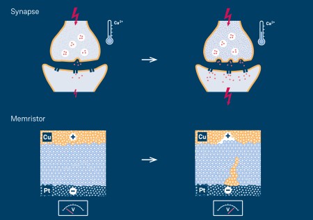
Electronic circuits in these ‘neuromorphic’ computers include memristors that resemble the junctions between neurons called synapses. Energy flows through a material from one electrode to another, much like a neuron firing a signal across the synapse to the next neuron. Scientists are now finding ways to better tune this intermediate material so the information flow is more stable and reliable.

I had no success locating the original news release, which originated the news item, but have found this May 17, 2021 news item on eedesignit.com, which provides the remaining portion of the news release.

“Oxides are the most widely used materials in memristors,” said Zhuge. “But oxide memristors have unsatisfactory stability and reliability. Oxide-based hybrid structures can effectively improve this.”

Memristors are usually made of an oxide-based material sandwiched between two electrodes. Researchers are getting better results when they combine two or more layers of different oxide-based materials between the electrodes. When an electrical current flows through the network, it induces ions to drift within the layers. The ions’ movements ultimately change the memristor’s resistance, which is necessary to send or stop a signal through the junction.

Memristors can be tuned further by changing the compounds used for electrodes or by adjusting the intermediate oxide-based materials. Zhuge and his team are currently developing optoelectronic neuromorphic computers based on optically-controlled oxide memristors. Compared to electronic memristors, photonic ones are expected to have higher operation speeds and lower energy consumption. They could be used to construct next generation artificial visual systems with high computing efficiency.

Now for a picture that accompanied the news release, which follows,

Fig. The all-optically controlled memristor developed for optoelectronic neuromorphic computing (Image by NIMTE)

Here’s the February 7, 2021 Ningbo Institute of Materials Technology and Engineering (NIMTE) press release featuring this work and a more technical description,

A research group led by Prof. ZHUGE Fei at the Ningbo Institute of Materials Technology and Engineering (NIMTE) of the Chinese Academy of Sciences (CAS) developed an all-optically controlled (AOC) analog memristor, whose memconductance can be reversibly tuned by varying only the wavelength of the controlling light.

As the next generation of artificial intelligence (AI), neuromorphic computing (NC) emulates the neural structure and operation of the human brain at the physical level, and thus can efficiently perform multiple advanced computing tasks such as learning, recognition and cognition.

Memristors are promising candidates for NC thanks to the feasibility of high-density 3D integration and low energy consumption. Among them, the emerging optoelectronic memristors are competitive by virtue of combining the advantages of both photonics and electronics. However, the reversible tuning of memconductance depends highly on the electric excitation, which have severely limited the development and application of optoelectronic NC.

To address this issue, researchers at NIMTE proposed a bilayered oxide AOC memristor, based on the relatively mature semiconductor material InGaZnO and a memconductance tuning mechanism of light-induced electron trapping and detrapping.

The traditional electrical memristors require strong electrical stimuli to tune their memconductance, leading to high power consumption, a large amount of Joule heat, microstructural change triggered by the Joule heat, and even high crosstalk in memristor crossbars.

On the contrary, the developed AOC memristor does not involve microstructure changes, and can operate upon weak light irradiation with light power density of only 20 μW cm-2, which has provided a new approach to overcome the instability of the memristor.

Specifically, the AOC memristor can serve as an excellent synaptic emulator and thus mimic spike-timing-dependent plasticity (STDP) which is an important learning rule in the brain, indicating its potential applications in AOC spiking neural networks for high-efficiency optoelectronic NC.

Moreover, compared to purely optical computing, the optoelectronic computing using our AOC memristor showed higher practical feasibility, on account of the simple structure and fabrication process of the device.

The study may shed light on the in-depth research and practical application of optoelectronic NC, and thus promote the development of the new generation of AI.

This work was supported by the National Natural Science Foundation of China (No. 61674156 and 61874125), the Strategic Priority Research Program of Chinese Academy of Sciences (No. XDB32050204), and the Zhejiang Provincial Natural Science Foundation of China (No. LD19E020001).

Here’s a link to and a citation for the paper,

Hybrid oxide brain-inspired neuromorphic devices for hardware implementation of artificial intelligence by Jingrui Wang, Xia Zhuge & Fei Zhuge. Science and Technology of Advanced Materials Volume 22, 2021 – Issue 1 Pages 326-344 DOI: https://doi.org/10.1080/14686996.2021.1911277 Published online:14 May 2021

This paper appears to be open access.

Netherlands

In this case, a May 18, 2021 news item on Nanowerk marries oxides to spintronics,

Classic computers use binary values (0/1) to perform. By contrast, our brain cells can use more values to operate, making them more energy-efficient than computers. This is why scientists are interested in neuromorphic (brain-like) computing.

Physicists from the University of Groningen (the Netherlands) have used a complex oxide to create elements comparable to the neurons and synapses in the brain using spins, a magnetic property of electrons.

The press release, which follows, was accompanied by this image illustrating the work,

Caption: Schematic of the proposed device structure for neuromorphic spintronic memristors. The write path is between the terminals through the top layer (black dotted line), the read path goes through the device stack (red dotted line). The right side of the figure indicates how the choice of substrate dictates whether the device will show deterministic or probabilistic behaviour. Credit: Banerjee group, University of Groningen

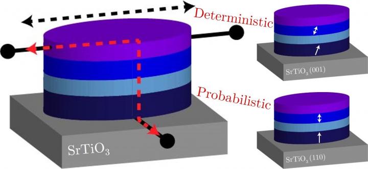
A May 18, 2021 University of Groningen press release (also on EurekAlert), which originated the news item, adds more ‘spin’ to the story,

Although computers can do straightforward calculations much faster than humans, our brains outperform silicon machines in tasks like object recognition. Furthermore, our brain uses less energy than computers. Part of this can be explained by the way our brain operates: whereas a computer uses a binary system (with values 0 or 1), brain cells can provide more analogue signals with a range of values.

Thin films

The operation of our brains can be simulated in computers, but the basic architecture still relies on a binary system. That is why scientist look for ways to expand this, creating hardware that is more brain-like, but will also interface with normal computers. ‘One idea is to create magnetic bits that can have intermediate states’, says Tamalika Banerjee, Professor of Spintronics of Functional Materials at the Zernike Institute for Advanced Materials, University of Groningen. She works on spintronics, which uses a magnetic property of electrons called ‘spin’ to transport, manipulate and store information.

In this study, her PhD student Anouk Goossens, first author of the paper, created thin films of a ferromagnetic metal (strontium-ruthenate oxide, SRO) grown on a substrate of strontium titanate oxide. The resulting thin film contained magnetic domains that were perpendicular to the plane of the film. ‘These can be switched more efficiently than in-plane magnetic domains’, explains Goossens. By adapting the growth conditions, it is possible to control the crystal orientation in the SRO. Previously, out-of-plane magnetic domains have been made using other techniques, but these typically require complex layer structures.

Magnetic anisotropy

The magnetic domains can be switched using a current through a platinum electrode on top of the SRO. Goossens: ‘When the magnetic domains are oriented perfectly perpendicular to the film, this switching is deterministic: the entire domain will switch.’ However, when the magnetic domains are slightly tilted, the response is probabilistic: not all the domains are the same, and intermediate values occur when only part of the crystals in the domain have switched.

By choosing variants of the substrate on which the SRO is grown, the scientists can control its magnetic anisotropy. This allows them to produce two different spintronic devices. ‘This magnetic anisotropy is exactly what we wanted’, says Goossens. ‘Probabilistic switching compares to how neurons function, while the deterministic switching is more like a synapse.’

The scientists expect that in the future, brain-like computer hardware can be created by combining these different domains in a spintronic device that can be connected to standard silicon-based circuits. Furthermore, probabilistic switching would also allow for stochastic computing, a promising technology which represents continuous values by streams of random bits. Banerjee: ‘We have found a way to control intermediate states, not just for memory but also for computing.’

Here’s a link to and a citation for the paper,

Anisotropy and Current Control of Magnetization in SrRuO3/SrTiO3 Heterostructures for Spin-Memristors by A.S. Goossens, M.A.T. Leiviskä and T. Banerjee. Frontiers in Nanotechnology DOI: https://doi.org/10.3389/fnano.2021.680468 Published: 18 May 2021

This appears to be open access.

New design directions to increase variety, efficiency, selectivity and reliability for memristive devices

A May 11, 2020 news item on ScienceDaily provides a description of the current ‘memristor scene’ along with an announcement about a piece of recent research,

Scientists around the world are intensively working on memristive devices, which are capable in extremely low power operation and behave similarly to neurons in the brain. Researchers from the Jülich Aachen Research Alliance (JARA) and the German technology group Heraeus have now discovered how to systematically control the functional behaviour of these elements. The smallest differences in material composition are found crucial: differences so small that until now experts had failed to notice them. The researchers’ design directions could help to increase variety, efficiency, selectivity and reliability for memristive technology-based applications, for example for energy-efficient, non-volatile storage devices or neuro-inspired computers.

Memristors are considered a highly promising alternative to conventional nanoelectronic elements in computer Chips [sic]. Because of the advantageous functionalities, their development is being eagerly pursued by many companies and research institutions around the world. The Japanese corporation NEC installed already the first prototypes in space satellites back in 2017. Many other leading companies such as Hewlett Packard, Intel, IBM, and Samsung are working to bring innovative types of computer and storage devices based on memristive elements to market.

Fundamentally, memristors are simply “resistors with memory,” in which high resistance can be switched to low resistance and back again. This means in principle that the devices are adaptive, similar to a synapse in a biological nervous system. “Memristive elements are considered ideal candidates for neuro-inspired computers modelled on the brain, which are attracting a great deal of interest in connection with deep learning and artificial intelligence,” says Dr. Ilia Valov of the Peter Grünberg Institute (PGI-7) at Forschungszentrum Jülich.

In the latest issue of the open access journal Science Advances, he and his team describe how the switching and neuromorphic behaviour of memristive elements can be selectively controlled. According to their findings, the crucial factor is the purity of the switching oxide layer. “Depending on whether you use a material that is 99.999999 % pure, and whether you introduce one foreign atom into ten million atoms of pure material or into one hundred atoms, the properties of the memristive elements vary substantially” says Valov.

A May 11, 2020 Forschungszentrum Juelich press release (also on EurekAlert), which originated the news item, delves into the theme of increasing control over memristive systems,

This effect had so far been overlooked by experts. It can be used very specifically for designing memristive systems, in a similar way to doping semiconductors in information technology. “The introduction of foreign atoms allows us to control the solubility and transport properties of the thin oxide layers,” explains Dr. Christian Neumann of the technology group Heraeus. He has been contributing his materials expertise to the project ever since the initial idea was conceived in 2015.

“In recent years there has been remarkable progress in the development and use of memristive devices, however that progress has often been achieved on a purely empirical basis,” according to Valov. Using the insights that his team has gained, manufacturers could now methodically develop memristive elements selecting the functions they need. The higher the doping concentration, the slower the resistance of the elements changes as the number of incoming voltage pulses increases and decreases, and the more stable the resistance remains. “This means that we have found a way for designing types of artificial synapses with differing excitability,” explains Valov.

Design specification for artificial synapses

The brain’s ability to learn and retain information can largely be attributed to the fact that the connections between neurons are strengthened when they are frequently used. Memristive devices, of which there are different types such as electrochemical metallization cells (ECMs) or valence change memory cells (VCMs), behave similarly. When these components are used, the conductivity increases as the number of incoming voltage pulses increases. The changes can also be reversed by applying voltage pulses of the opposite polarity.

The JARA researchers conducted their systematic experiments on ECMs, which consist of a copper electrode, a platinum electrode, and a layer of silicon dioxide between them. Thanks to the cooperation with Heraeus researchers, the JARA scientists had access to different types of silicon dioxide: one with a purity of 99.999999 % – also called 8N silicon dioxide – and others containing 100 to 10,000 ppm (parts per million) of foreign atoms. The precisely doped glass used in their experiments was specially developed and manufactured by quartz glass specialist Heraeus Conamic, which also holds the patent for the procedure. Copper and protons acted as mobile doping agents, while aluminium and gallium were used as non-volatile doping.

Synapses, the connections between neurons, have the ability to transmit signals with varying degrees of strength when they are excited by a quick succession of electrical impulses. One effect of this repeated activity is to increase the concentration of calcium ions, with the result that more neurotransmitters are emitted. Depending on the activity, other effects cause long-term structural changes, which impact the strength of the transmission for several hours, or potentially even for the rest of the person’s life. Memristive elements allow the strength of the electrical transmission to be changed in a similar way to synaptic connections, by applying a voltage. In electrochemical metallization cells (ECMs), a metallic filament develops between the two metal electrodes, thus increasing conductivity. Applying voltage pulses with reversed polarity causes the filament to shrink again until the cell reaches its initial high resistance state. Copyright: Forschungszentrum Jülich / Tobias Schlößer

Record switching time confirms theory

Based on their series of experiments, the researchers were able to show that the ECMs’ switching times change as the amount of doping atoms changes. If the switching layer is made of 8N silicon dioxide, the memristive component switches in only 1.4 nanoseconds. To date, the fastest value ever measured for ECMs had been around 10 nanoseconds. By doping the oxide layer of the components with up to 10,000 ppm of foreign atoms, the switching time was prolonged into the range of milliseconds. “We can also theoretically explain our results. This is helping us to understand the physico-chemical processes on the nanoscale and apply this knowledge in the practice” says Valov. Based on generally applicable theoretical considerations, supported by experimental results, some also documented in the literature, he is convinced that the doping/impurity effect occurs and can be employed in all types memristive elements.

Top: In memristive elements (ECMs) with an undoped, high-purity switching layer of silicon oxide (SiO2), copper ions can move very fast. A filament of copper atoms forms correspondingly fast on the platinum electrode. This increases the total device conductivity respectively the capacity. Due to the high mobility of the ions, however, this filament is unstable at low forming voltages. Center: Gallium ions (Ga3+), which are introduced into the cell (non-volatile doping), bind copper ions (Cu2+) in the switching layer. The movement of the ions slows down, leading to lower switching times, but the filament, once formed remains longer stable. Bottom: Doping with aluminium ions (Al3+) slows down the process even more, since aluminium ions bind copper ions even stronger than gallium ions. Filament growth is even slower, while at the same time the stability of the filament is further increased. Depending on the chemical properties of the introduced doping elements, memristive cells – the artificial synapses – can be created with tailor-made switching and neuromorphic properties. Copyright: Forschungszentrum Jülich / Tobias Schloesser

Here’s a link to and a citation for the paper,

Design of defect-chemical properties and device performance in memristive systems by M. Lübben, F. Cüppers, J. Mohr, M. von Witzleben, U. Breuer, R. Waser, C. Neumann, and I. Valov. Science Advances 08 May 2020: Vol. 6, no. 19, eaaz9079 DOI: 10.1126/sciadv.aaz9079

This paper is open access.

For anyone curious about the German technology group, Heraeus, there’s a fascinating history in its Wikipedia entry. The technology company was formally founded in 1851 but it can be traced back to the 17th century and the founding family’s apothecary.

An artificial synapse tuned by light, a ferromagnetic memristor, and a transparent, flexible artificial synapse

Down the memristor rabbit hole one more time.* I started out with news about two new papers and inadvertently found two more. In a bid to keep this posting to a manageable size, I’m stopping at four.

UK

In a June 19, 2019 Nanowerk Spotlight article, Dr. Neil Kemp discusses memristors and some of his latest work (Note: A link has been removed),

Memristor (or memory resistors) devices are non-volatile electronic memory devices that were first theorized by Leon Chua in the 1970’s. However, it was some thirty years later that the first practical device was fabricated. This was in 2008 when a group led by Stanley Williams at HP Research Labs realized that switching of the resistance between a conducting and less conducting state in metal-oxide thin-film devices was showing Leon Chua’s memristor behaviour.

The high interest in memristor devices also stems from the fact that these devices emulate the memory and learning properties of biological synapses. i.e. the electrical resistance value of the device is dependent on the history of the current flowing through it.

There is a huge effort underway to use memristor devices in neuromorphic computing applications and it is now reasonable to imagine the development of a new generation of artificial intelligent devices with very low power consumption (non-volatile), ultra-fast performance and high-density integration.

These discoveries come at an important juncture in microelectronics, since there is increasing disparity between computational needs of Big Data, Artificial Intelligence (A.I.) and the Internet of Things (IoT), and the capabilities of existing computers. The increases in speed, efficiency and performance of computer technology cannot continue in the same manner as it has done since the 1960s.

To date, most memristor research has focussed on the electronic switching properties of the device. However, for many applications it is useful to have an additional handle (or degree of freedom) on the device to control its resistive state. For example memory and processing in the brain also involves numerous chemical and bio-chemical reactions that control the brain structure and its evolution through development.

To emulate this in a simple solid-state system composed of just switches alone is not possible. In our research, we are interested in using light to mediate this essential control.

We have demonstrated that light can be used to make short and long-term memory and we have shown how light can modulate a special type of learning, called spike timing dependent plasticity (STDP). STDP involves two neuronal spikes incident across a synapse at the same time. Depending on the relative timing of the spikes and their overlap across the synaptic cleft, the connection strength is other strengthened or weakened.

In our earlier work, we were only able to achieve to small switching effects in memristors using light. In our latest work (Advanced Electronic Materials, “Percolation Threshold Enables Optical Resistive-Memory Switching and Light-Tuneable Synaptic Learning in Segregated Nanocomposites”), we take advantage of a percolating-like nanoparticle morphology to vastly increase the magnitude of the switching between electronic resistance states when light is incident on the device.

We have used an inhomogeneous percolating network consisting of metallic nanoparticles distributed in filamentary-like conduction paths. Electronic conduction and the resistance of the device is very sensitive to any disruption of the conduction path(s).

By embedding the nanoparticles in a polymer that can expand or contract with light the conduction pathways are broken or re-connected causing very large changes in the electrical resistance and memristance of the device.

Our devices could lead to the development of new memristor-based artificial intelligence systems that are adaptive and reconfigurable using a combination of optical and electronic signalling. Furthermore, they have the potential for the development of very fast optical cameras for artificial intelligence recognition systems.

Our work provides a nice proof-of-concept but the materials used means the optical switching is slow. The materials are also not well suited to industry fabrication. In our on-going work we are addressing these switching speed issues whilst also focussing on industry compatible materials.

Currently we are working on a new type of optical memristor device that should give us orders of magnitude improvement in the optical switching speeds whilst also retaining a large difference between the resistance on and off states. We hope to be able to achieve nanosecond switching speeds. The materials used are also compatible with industry standard methods of fabrication.

The new devices should also have applications in optical communications, interfacing and photonic computing. We are currently looking for commercial investors to help fund the research on these devices so that we can bring the device specifications to a level of commercial interest.

If you’re interested in memristors, Kemp’s article is well written and quite informative for nonexperts, assuming of course you can tolerate not understanding everything perfectly.

Here are links and citations for two papers. The first is the latest referred to in the article, a May 2019 paper and the second is a paper appearing in July 2019.

Percolation Threshold Enables Optical Resistive‐Memory Switching and Light‐Tuneable Synaptic Learning in Segregated Nanocomposites by Ayoub H. Jaafar, Mary O’Neill, Stephen M. Kelly, Emanuele Verrelli, Neil T. Kemp. Advanced Electronic Materials DOI: https://doi.org/10.1002/aelm.201900197 First published: 28 May 2019

Wavelength dependent light tunable resistive switching graphene oxide nonvolatile memory devices by Ayoub H.Jaafar, N.T.Kemp. DOI: https://doi.org/10.1016/j.carbon.2019.07.007 Carbon Available online 3 July 2019

The first paper (May 2019) is definitely behind a paywall and the second paper (July 2019) appears to be behind a paywall.

Dr. Kemp’s work has been featured here previously in a January 3, 2018 posting in the subsection titled, Shining a light on the memristor.

China

This work from China was announced in a June 20, 2019 news item on Nanowerk,

Memristors, demonstrated by solid-state devices with continuously tunable resistance, have emerged as a new paradigm for self-adaptive networks that require synapse-like functions. Spin-based memristors offer advantages over other types of memristors because of their significant endurance and high energy effciency.

However, it remains a challenge to build dense and functional spintronic memristors with structures and materials that are compatible with existing ferromagnetic devices. Ta/CoFeB/MgO heterostructures are commonly used in interfacial PMA-based [perpendicular magnetic anisotropy] magnetic tunnel junctions, which exhibit large tunnel magnetoresistance and are implemented in commercial MRAM [magnetic random access memory] products.

“To achieve the memristive function, DW is driven back and forth in a continuous manner in the CoFeB layer by applying in-plane positive or negative current pulses along the Ta layer, utilizing SOT that the current exerts on the CoFeB magnetization,” said Shuai Zhang, a coauthor in the paper. “Slowly propagating domain wall generates a creep in the detection area of the device, which yields a broad range of intermediate resistive states in the AHE [anomalous Hall effect] measurements. Consequently, AHE resistance is modulated in an analog manner, being controlled by the pulsed current characteristics including amplitude, duration, and repetition number.”

“For a follow-up study, we are working on more neuromorphic operations, such as spike-timing-dependent plasticity and paired pulsed facilitation,” concludes You. …

Here’s are links to and citations for the paper (Note: It’s a little confusing but I believe that one of the links will take you to the online version, as for the ‘open access’ link, keep reading),

A Spin–Orbit‐Torque Memristive Device by Shuai Zhang, Shijiang Luo, Nuo Xu, Qiming Zou, Min Song, Jijun Yun, Qiang Luo, Zhe Guo, Ruofan Li, Weicheng Tian, Xin Li, Hengan Zhou, Huiming Chen, Yue Zhang, Xiaofei Yang, Wanjun Jiang, Ka Shen, Jeongmin Hong, Zhe Yuan, Li Xi, Ke Xia, Sayeef Salahuddin, Bernard Dieny, Long You. Advanced Electronic Materials Volume 5, Issue 4 April 2019 (print version) 1800782 DOI: https://doi.org/10.1002/aelm.201800782 First published [online]: 30 January 2019 Note: there is another DOI, https://doi.org/10.1002/aelm.201970022 where you can have open access to Memristors: A Spin–Orbit‐Torque Memristive Device (Adv. Electron. Mater. 4/2019)

The paper published online in January 2019 is behind a paywall and the paper (almost the same title) published in April 2019 has a new DOI and is open access. Final note: I tried accessing the ‘free’ paper and opened up a free file for the artwork featuring the work from China on the back cover of the April 2019 of Advanced Electronic Materials.

Korea

Usually when I see the words transparency and flexibility, I expect to see graphene is one of the materials. That’s not the case for this paper (link to and citation for),

Transparent and flexible photonic artificial synapse with piezo-phototronic modulator: Versatile memory capability and higher order learning algorithm by Mohit Kumar, Joondong Kim, Ching-Ping Wong. Nano Energy Volume 63, September 2019, 103843 DOI: https://doi.org/10.1016/j.nanoen.2019.06.039 Available online 22 June 2019

Here’s the abstract for the paper where you’ll see that the material is made up of zinc oxide silver nanowires,

An artificial photonic synapse having tunable manifold synaptic response can be an essential step forward for the advancement of novel neuromorphic computing. In this work, we reported the development of highly transparent and flexible two-terminal ZnO/Ag-nanowires/PET photonic artificial synapse [emphasis mine]. The device shows purely photo-triggered all essential synaptic functions such as transition from short-to long-term plasticity, paired-pulse facilitation, and spike-timing-dependent plasticity, including in the versatile memory capability. Importantly, strain-induced piezo-phototronic effect within ZnO provides an additional degree of regulation to modulate all of the synaptic functions in multi-levels. The observed effect is quantitatively explained as a dynamic of photo-induced electron-hole trapping/detraining via the defect states such as oxygen vacancies. We revealed that the synaptic functions can be consolidated and converted by applied strain, which is not previously applied any of the reported synaptic devices. This study will open a new avenue to the scientific community to control and design highly transparent wearable neuromorphic computing.

This paper is behind a paywall.

Artificial synapse based on tantalum oxide from Korean researchers

This memristor story comes from South Korea as we progress on the way to neuromorphic computing (brainlike computing). A Sept. 7, 2018 news item on ScienceDaily makes the announcement,

A research team led by Director Myoung-Jae Lee from the Intelligent Devices and Systems Research Group at DGIST (Daegu Gyeongbuk Institute of Science and Technology) has succeeded in developing an artificial synaptic device that mimics the function of the nerve cells (neurons) and synapses that are response for memory in human brains. [sic]

Synapses are where axons and dendrites meet so that neurons in the human brain can send and receive nerve signals; there are known to be hundreds of trillions of synapses in the human brain.

This chemical synapse information transfer system, which transfers information from the brain, can handle high-level parallel arithmetic with very little energy, so research on artificial synaptic devices, which mimic the biological function of a synapse, is under way worldwide.

Dr. Lee’s research team, through joint research with teams led by Professor Gyeong-Su Park from Seoul National University; Professor Sung Kyu Park from Chung-ang University; and Professor Hyunsang Hwang from Pohang University of Science and Technology (POSTEC), developed a high-reliability artificial synaptic device with multiple values by structuring tantalum oxide — a trans-metallic material — into two layers of Ta2O5-x and TaO2-x and by controlling its surface.

A September 7, 2018 DGIST press release (also on EurekAlert), which originated the news item, delves further into the work,

The artificial synaptic device developed by the research team is an electrical synaptic device that simulates the function of synapses in the brain as the resistance of the tantalum oxide layer gradually increases or decreases depending on the strength of the electric signals. It has succeeded in overcoming durability limitations of current devices by allowing current control only on one layer of Ta2O5-x.

In addition, the research team successfully implemented an experiment that realized synapse plasticity [or synaptic plasticity], which is the process of creating, storing, and deleting memories, such as long-term strengthening of memory and long-term suppression of memory deleting by adjusting the strength of the synapse connection between neurons.

The non-volatile multiple-value data storage method applied by the research team has the technological advantage of having a small area of an artificial synaptic device system, reducing circuit connection complexity, and reducing power consumption by more than one-thousandth compared to data storage methods based on digital signals using 0 and 1 such as volatile CMOS (Complementary Metal Oxide Semiconductor).

The high-reliability artificial synaptic device developed by the research team can be used in ultra-low-power devices or circuits for processing massive amounts of big data due to its capability of low-power parallel arithmetic. It is expected to be applied to next-generation intelligent semiconductor device technologies such as development of artificial intelligence (AI) including machine learning and deep learning and brain-mimicking semiconductors.

Dr. Lee said, “This research secured the reliability of existing artificial synaptic devices and improved the areas pointed out as disadvantages. We expect to contribute to the development of AI based on the neuromorphic system that mimics the human brain by creating a circuit that imitates the function of neurons.”

Here’s a link to and a citation for the paper,

Reliable Multivalued Conductance States in TaOx Memristors through Oxygen Plasma-Assisted Electrode Deposition with in Situ-Biased Conductance State Transmission Electron Microscopy Analysis by Myoung-Jae Lee, Gyeong-Su Park, David H. Seo, Sung Min Kwon, Hyeon-Jun Lee, June-Seo Kim, MinKyung Jung, Chun-Yeol You, Hyangsook Lee, Hee-Goo Kim, Su-Been Pang, Sunae Seo, Hyunsang Hwang, and Sung Kyu Park. ACS Appl. Mater. Interfaces, 2018, 10 (35), pp 29757–29765 DOI: 10.1021/acsami.8b09046 Publication Date (Web): July 23, 2018

Copyright © 2018 American Chemical Society

This paper is open access.

You can find other memristor and neuromorphic computing stories here by using the search terms I’ve highlighted,  My latest (more or less) is an April 19, 2018 posting titled, New path to viable memristor/neuristor?

Finally, here’s an image from the Korean researchers that accompanied their work,

Caption: Representation of neurons and synapses in the human brain. The magnified synapse represents the portion mimicked using solid-state devices. Credit: Daegu Gyeongbuk Institute of Science and Technology(DGIST)

Brainy and brainy: a novel synaptic architecture and a neuromorphic computing platform called SpiNNaker

I have two items about brainlike computing. The first item hearkens back to memristors, a topic I have been following since 2008. (If you’re curious about the various twists and turns just enter  the term ‘memristor’ in this blog’s search engine.) The latest on memristors is from a team than includes IBM (US), École Politechnique Fédérale de Lausanne (EPFL; Swizterland), and the New Jersey Institute of Technology (NJIT; US). The second bit comes from a Jülich Research Centre team in Germany and concerns an approach to brain-like computing that does not include memristors.

Multi-memristive synapses

In the inexorable march to make computers function more like human brains (neuromorphic engineering/computing), an international team has announced its latest results in a July 10, 2018 news item on Nanowerk,

Two New Jersey Institute of Technology (NJIT) researchers, working with collaborators from the IBM Research Zurich Laboratory and the École Polytechnique Fédérale de Lausanne, have demonstrated a novel synaptic architecture that could lead to a new class of information processing systems inspired by the brain.

The findings are an important step toward building more energy-efficient computing systems that also are capable of learning and adaptation in the real world. …

A July 10, 2018 NJIT news release (also on EurekAlert) by Tracey Regan, which originated by the news item, adds more details,

The researchers, Bipin Rajendran, an associate professor of electrical and computer engineering, and S. R. Nandakumar, a graduate student in electrical engineering, have been developing brain-inspired computing systems that could be used for a wide range of big data applications.

Over the past few years, deep learning algorithms have proven to be highly successful in solving complex cognitive tasks such as controlling self-driving cars and language understanding. At the heart of these algorithms are artificial neural networks – mathematical models of the neurons and synapses of the brain – that are fed huge amounts of data so that the synaptic strengths are autonomously adjusted to learn the intrinsic features and hidden correlations in these data streams.

However, the implementation of these brain-inspired algorithms on conventional computers is highly inefficient, consuming huge amounts of power and time. This has prompted engineers to search for new materials and devices to build special-purpose computers that can incorporate the algorithms. Nanoscale memristive devices, electrical components whose conductivity depends approximately on prior signaling activity, can be used to represent the synaptic strength between the neurons in artificial neural networks.

While memristive devices could potentially lead to faster and more power-efficient computing systems, they are also plagued by several reliability issues that are common to nanoscale devices. Their efficiency stems from their ability to be programmed in an analog manner to store multiple bits of information; however, their electrical conductivities vary in a non-deterministic and non-linear fashion.

In the experiment, the team showed how multiple nanoscale memristive devices exhibiting these characteristics could nonetheless be configured to efficiently implement artificial intelligence algorithms such as deep learning. Prototype chips from IBM containing more than one million nanoscale phase-change memristive devices were used to implement a neural network for the detection of hidden patterns and correlations in time-varying signals.

“In this work, we proposed and experimentally demonstrated a scheme to obtain high learning efficiencies with nanoscale memristive devices for implementing learning algorithms,” Nandakumar says. “The central idea in our demonstration was to use several memristive devices in parallel to represent the strength of a synapse of a neural network, but only chose one of them to be updated at each step based on the neuronal activity.”

Here’s a link to and a citation for the paper,

Neuromorphic computing with multi-memristive synapses by Irem Boybat, Manuel Le Gallo, S. R. Nandakumar, Timoleon Moraitis, Thomas Parnell, Tomas Tuma, Bipin Rajendran, Yusuf Leblebici, Abu Sebastian, & Evangelos Eleftheriou. Nature Communications volume 9, Article number: 2514 (2018) DOI: https://doi.org/10.1038/s41467-018-04933-y Published 28 June 2018

This is an open access paper.

Also they’ve got a couple of very nice introductory paragraphs which I’m including here, (from the June 28, 2018 paper in Nature Communications; Note: Links have been removed),

The human brain with less than 20 W of power consumption offers a processing capability that exceeds the petaflops mark, and thus outperforms state-of-the-art supercomputers by several orders of magnitude in terms of energy efficiency and volume. Building ultra-low-power cognitive computing systems inspired by the operating principles of the brain is a promising avenue towards achieving such efficiency. Recently, deep learning has revolutionized the field of machine learning by providing human-like performance in areas, such as computer vision, speech recognition, and complex strategic games1. However, current hardware implementations of deep neural networks are still far from competing with biological neural systems in terms of real-time information-processing capabilities with comparable energy consumption.

One of the reasons for this inefficiency is that most neural networks are implemented on computing systems based on the conventional von Neumann architecture with separate memory and processing units. There are a few attempts to build custom neuromorphic hardware that is optimized to implement neural algorithms2,3,4,5. However, as these custom systems are typically based on conventional silicon complementary metal oxide semiconductor (CMOS) circuitry, the area efficiency of such hardware implementations will remain relatively low, especially if in situ learning and non-volatile synaptic behavior have to be incorporated. Recently, a new class of nanoscale devices has shown promise for realizing the synaptic dynamics in a compact and power-efficient manner. These memristive devices store information in their resistance/conductance states and exhibit conductivity modulation based on the programming history6,7,8,9. The central idea in building cognitive hardware based on memristive devices is to store the synaptic weights as their conductance states and to perform the associated computational tasks in place.

The two essential synaptic attributes that need to be emulated by memristive devices are the synaptic efficacy and plasticity. …

It gets more complicated from there.

Now onto the next bit.

SpiNNaker

At a guess, those capitalized N’s are meant to indicate ‘neural networks’. As best I can determine, SpiNNaker is not based on the memristor. Moving on, a July 11, 2018 news item on phys.org announces work from a team examining how neuromorphic hardware and neuromorphic software work together,

A computer built to mimic the brain’s neural networks produces similar results to that of the best brain-simulation supercomputer software currently used for neural-signaling research, finds a new study published in the open-access journal Frontiers in Neuroscience. Tested for accuracy, speed and energy efficiency, this custom-built computer named SpiNNaker, has the potential to overcome the speed and power consumption problems of conventional supercomputers. The aim is to advance our knowledge of neural processing in the brain, to include learning and disorders such as epilepsy and Alzheimer’s disease.

A July 11, 2018 Frontiers Publishing news release on EurekAlert, which originated the news item, expands on the latest work,

“SpiNNaker can support detailed biological models of the cortex–the outer layer of the brain that receives and processes information from the senses–delivering results very similar to those from an equivalent supercomputer software simulation,” says Dr. Sacha van Albada, lead author of this study and leader of the Theoretical Neuroanatomy group at the Jülich Research Centre, Germany. “The ability to run large-scale detailed neural networks quickly and at low power consumption will advance robotics research and facilitate studies on learning and brain disorders.”

The human brain is extremely complex, comprising 100 billion interconnected brain cells. We understand how individual neurons and their components behave and communicate with each other and on the larger scale, which areas of the brain are used for sensory perception, action and cognition. However, we know less about the translation of neural activity into behavior, such as turning thought into muscle movement.

Supercomputer software has helped by simulating the exchange of signals between neurons, but even the best software run on the fastest supercomputers to date can only simulate 1% of the human brain.

“It is presently unclear which computer architecture is best suited to study whole-brain networks efficiently. The European Human Brain Project and Jülich Research Centre have performed extensive research to identify the best strategy for this highly complex problem. Today’s supercomputers require several minutes to simulate one second of real time, so studies on processes like learning, which take hours and days in real time are currently out of reach.” explains Professor Markus Diesmann, co-author, head of the Computational and Systems Neuroscience department at the Jülich Research Centre.

He continues, “There is a huge gap between the energy consumption of the brain and today’s supercomputers. Neuromorphic (brain-inspired) computing allows us to investigate how close we can get to the energy efficiency of the brain using electronics.”

Developed over the past 15 years and based on the structure and function of the human brain, SpiNNaker — part of the Neuromorphic Computing Platform of the Human Brain Project — is a custom-built computer composed of half a million of simple computing elements controlled by its own software. The researchers compared the accuracy, speed and energy efficiency of SpiNNaker with that of NEST–a specialist supercomputer software currently in use for brain neuron-signaling research.

“The simulations run on NEST and SpiNNaker showed very similar results,” reports Steve Furber, co-author and Professor of Computer Engineering at the University of Manchester, UK. “This is the first time such a detailed simulation of the cortex has been run on SpiNNaker, or on any neuromorphic platform. SpiNNaker comprises 600 circuit boards incorporating over 500,000 small processors in total. The simulation described in this study used just six boards–1% of the total capability of the machine. The findings from our research will improve the software to reduce this to a single board.”

Van Albada shares her future aspirations for SpiNNaker, “We hope for increasingly large real-time simulations with these neuromorphic computing systems. In the Human Brain Project, we already work with neuroroboticists who hope to use them for robotic control.”

Before getting to the link and citation for the paper, here’s a description of SpiNNaker’s hardware from the ‘Spiking neural netowrk’ Wikipedia entry, Note: Links have been removed,

Neurogrid, built at Stanford University, is a board that can simulate spiking neural networks directly in hardware. SpiNNaker (Spiking Neural Network Architecture) [emphasis mine], designed at the University of Manchester, uses ARM processors as the building blocks of a massively parallel computing platform based on a six-layer thalamocortical model.[5]

Now for the link and citation,

Performance Comparison of the Digital Neuromorphic Hardware SpiNNaker and the Neural Network Simulation Software NEST for a Full-Scale Cortical Microcircuit Model by
Sacha J. van Albada, Andrew G. Rowley, Johanna Senk, Michael Hopkins, Maximilian Schmidt, Alan B. Stokes, David R. Lester, Markus Diesmann, and Steve B. Furber. Neurosci. 12:291. doi: 10.3389/fnins.2018.00291 Published: 23 May 2018

As noted earlier, this is an open access paper.

New path to viable memristor/neuristor?

I first stumbled onto memristors and the possibility of brain-like computing sometime in 2008 (around the time that R. Stanley Williams and his team at HP Labs first published the results of their research linking Dr. Leon Chua’s memristor theory to their attempts to shrink computer chips). In the almost 10 years since, scientists have worked hard to utilize memristors in the field of neuromorphic (brain-like) engineering/computing.

A January 22, 2018 news item on phys.org describes the latest work,

When it comes to processing power, the human brain just can’t be beat.

Packed within the squishy, football-sized organ are somewhere around 100 billion neurons. At any given moment, a single neuron can relay instructions to thousands of other neurons via synapses—the spaces between neurons, across which neurotransmitters are exchanged. There are more than 100 trillion synapses that mediate neuron signaling in the brain, strengthening some connections while pruning others, in a process that enables the brain to recognize patterns, remember facts, and carry out other learning tasks, at lightning speeds.

Researchers in the emerging field of “neuromorphic computing” have attempted to design computer chips that work like the human brain. Instead of carrying out computations based on binary, on/off signaling, like digital chips do today, the elements of a “brain on a chip” would work in an analog fashion, exchanging a gradient of signals, or “weights,” much like neurons that activate in various ways depending on the type and number of ions that flow across a synapse.

In this way, small neuromorphic chips could, like the brain, efficiently process millions of streams of parallel computations that are currently only possible with large banks of supercomputers. But one significant hangup on the way to such portable artificial intelligence has been the neural synapse, which has been particularly tricky to reproduce in hardware.

Now engineers at MIT [Massachusetts Institute of Technology] have designed an artificial synapse in such a way that they can precisely control the strength of an electric current flowing across it, similar to the way ions flow between neurons. The team has built a small chip with artificial synapses, made from silicon germanium. In simulations, the researchers found that the chip and its synapses could be used to recognize samples of handwriting, with 95 percent accuracy.

A January 22, 2018 MIT news release by Jennifer Chua (also on EurekAlert), which originated the news item, provides more detail about the research,

The design, published today [January 22, 2018] in the journal Nature Materials, is a major step toward building portable, low-power neuromorphic chips for use in pattern recognition and other learning tasks.

The research was led by Jeehwan Kim, the Class of 1947 Career Development Assistant Professor in the departments of Mechanical Engineering and Materials Science and Engineering, and a principal investigator in MIT’s Research Laboratory of Electronics and Microsystems Technology Laboratories. His co-authors are Shinhyun Choi (first author), Scott Tan (co-first author), Zefan Li, Yunjo Kim, Chanyeol Choi, and Hanwool Yeon of MIT, along with Pai-Yu Chen and Shimeng Yu of Arizona State University.

Too many paths

Most neuromorphic chip designs attempt to emulate the synaptic connection between neurons using two conductive layers separated by a “switching medium,” or synapse-like space. When a voltage is applied, ions should move in the switching medium to create conductive filaments, similarly to how the “weight” of a synapse changes.

But it’s been difficult to control the flow of ions in existing designs. Kim says that’s because most switching mediums, made of amorphous materials, have unlimited possible paths through which ions can travel — a bit like Pachinko, a mechanical arcade game that funnels small steel balls down through a series of pins and levers, which act to either divert or direct the balls out of the machine.

Like Pachinko, existing switching mediums contain multiple paths that make it difficult to predict where ions will make it through. Kim says that can create unwanted nonuniformity in a synapse’s performance.

“Once you apply some voltage to represent some data with your artificial neuron, you have to erase and be able to write it again in the exact same way,” Kim says. “But in an amorphous solid, when you write again, the ions go in different directions because there are lots of defects. This stream is changing, and it’s hard to control. That’s the biggest problem — nonuniformity of the artificial synapse.”

A perfect mismatch

Instead of using amorphous materials as an artificial synapse, Kim and his colleagues looked to single-crystalline silicon, a defect-free conducting material made from atoms arranged in a continuously ordered alignment. The team sought to create a precise, one-dimensional line defect, or dislocation, through the silicon, through which ions could predictably flow.

To do so, the researchers started with a wafer of silicon, resembling, at microscopic resolution, a chicken-wire pattern. They then grew a similar pattern of silicon germanium — a material also used commonly in transistors — on top of the silicon wafer. Silicon germanium’s lattice is slightly larger than that of silicon, and Kim found that together, the two perfectly mismatched materials can form a funnel-like dislocation, creating a single path through which ions can flow.

The researchers fabricated a neuromorphic chip consisting of artificial synapses made from silicon germanium, each synapse measuring about 25 nanometers across. They applied voltage to each synapse and found that all synapses exhibited more or less the same current, or flow of ions, with about a 4 percent variation between synapses — a much more uniform performance compared with synapses made from amorphous material.

They also tested a single synapse over multiple trials, applying the same voltage over 700 cycles, and found the synapse exhibited the same current, with just 1 percent variation from cycle to cycle.

“This is the most uniform device we could achieve, which is the key to demonstrating artificial neural networks,” Kim says.

Writing, recognized

As a final test, Kim’s team explored how its device would perform if it were to carry out actual learning tasks — specifically, recognizing samples of handwriting, which researchers consider to be a first practical test for neuromorphic chips. Such chips would consist of “input/hidden/output neurons,” each connected to other “neurons” via filament-based artificial synapses.

Scientists believe such stacks of neural nets can be made to “learn.” For instance, when fed an input that is a handwritten ‘1,’ with an output that labels it as ‘1,’ certain output neurons will be activated by input neurons and weights from an artificial synapse. When more examples of handwritten ‘1s’ are fed into the same chip, the same output neurons may be activated when they sense similar features between different samples of the same letter, thus “learning” in a fashion similar to what the brain does.

Kim and his colleagues ran a computer simulation of an artificial neural network consisting of three sheets of neural layers connected via two layers of artificial synapses, the properties of which they based on measurements from their actual neuromorphic chip. They fed into their simulation tens of thousands of samples from a handwritten recognition dataset commonly used by neuromorphic designers, and found that their neural network hardware recognized handwritten samples 95 percent of the time, compared to the 97 percent accuracy of existing software algorithms.

The team is in the process of fabricating a working neuromorphic chip that can carry out handwriting-recognition tasks, not in simulation but in reality. Looking beyond handwriting, Kim says the team’s artificial synapse design will enable much smaller, portable neural network devices that can perform complex computations that currently are only possible with large supercomputers.

“Ultimately we want a chip as big as a fingernail to replace one big supercomputer,” Kim says. “This opens a stepping stone to produce real artificial hardware.”

This research was supported in part by the National Science Foundation.

Here’s a link to and a citation for the paper,

SiGe epitaxial memory for neuromorphic computing with reproducible high performance based on engineered dislocations by Shinhyun Choi, Scott H. Tan, Zefan Li, Yunjo Kim, Chanyeol Choi, Pai-Yu Chen, Hanwool Yeon, Shimeng Yu, & Jeehwan Kim. Nature Materials (2018) doi:10.1038/s41563-017-0001-5 Published online: 22 January 2018

This paper is behind a paywall.

For the curious I have included a number of links to recent ‘memristor’ postings here,

January 22, 2018: Memristors at Masdar

January 3, 2018: Mott memristor

August 24, 2017: Neuristors and brainlike computing

June 28, 2017: Dr. Wei Lu and bio-inspired ‘memristor’ chips

May 2, 2017: Predicting how a memristor functions

December 30, 2016: Changing synaptic connectivity with a memristor

December 5, 2016: The memristor as computing device

November 1, 2016: The memristor as the ‘missing link’ in bioelectronic medicine?

You can find more by using ‘memristor’ as the search term in the blog search function or on the search engine of your choice.

Carbon nanotubes to repair nerve fibres (cyborg brains?)

Can cyborg brains be far behind now that researchers are looking at ways to repair nerve fibers with carbon nanotubes (CNTs)? A June 26, 2017 news item on ScienceDaily describes the scheme using carbon nanotubes as a material for repairing nerve fibers,

Carbon nanotubes exhibit interesting characteristics rendering them particularly suited to the construction of special hybrid devices — consisting of biological issue and synthetic material — planned to re-establish connections between nerve cells, for instance at spinal level, lost on account of lesions or trauma. This is the result of a piece of research published on the scientific journal Nanomedicine: Nanotechnology, Biology, and Medicine conducted by a multi-disciplinary team comprising SISSA (International School for Advanced Studies), the University of Trieste, ELETTRA Sincrotrone and two Spanish institutions, Basque Foundation for Science and CIC BiomaGUNE. More specifically, researchers have investigated the possible effects on neurons of the interaction with carbon nanotubes. Scientists have proven that these nanomaterials may regulate the formation of synapses, specialized structures through which the nerve cells communicate, and modulate biological mechanisms, such as the growth of neurons, as part of a self-regulating process. This result, which shows the extent to which the integration between nerve cells and these synthetic structures is stable and efficient, highlights the great potentialities of carbon nanotubes as innovative materials capable of facilitating neuronal regeneration or in order to create a kind of artificial bridge between groups of neurons whose connection has been interrupted. In vivo testing has actually already begun.

The researchers have included a gorgeous image to illustrate their work,

Caption: Scientists have proven that these nanomaterials may regulate the formation of synapses, specialized structures through which the nerve cells communicate, and modulate biological mechanisms, such as the growth of neurons, as part of a self-regulating process. Credit: Pixabay

A June 26, 2017 SISSA press release (also on EurekAlert), which originated the news item, describes the work in more detail while explaining future research needs,

“Interface systems, or, more in general, neuronal prostheses, that enable an effective re-establishment of these connections are under active investigation” explain Laura Ballerini (SISSA) and Maurizio Prato (UniTS-CIC BiomaGUNE), coordinating the research project. “The perfect material to build these neural interfaces does not exist, yet the carbon nanotubes we are working on have already proved to have great potentialities. After all, nanomaterials currently represent our best hope for developing innovative strategies in the treatment of spinal cord injuries”. These nanomaterials are used both as scaffolds, a supportive framework for nerve cells, and as means of interfaces releasing those signals that empower nerve cells to communicate with each other.

Many aspects, however, still need to be addressed. Among them, the impact on neuronal physiology of the integration of these nanometric structures with the cell membrane. “Studying the interaction between these two elements is crucial, as it might also lead to some undesired effects, which we ought to exclude”. Laura Ballerini explains: “If, for example, the mere contact provoked a vertiginous rise in the number of synapses, these materials would be essentially unusable”. “This”, Maurizio Prato adds, “is precisely what we have investigated in this study where we used pure carbon nanotubes”.

The results of the research are extremely encouraging: “First of all we have proved that nanotubes do not interfere with the composition of lipids, of cholesterol in particular, which make up the cellular membrane in neurons. Membrane lipids play a very important role in the transmission of signals through the synapses. Nanotubes do not seem to influence this process, which is very important”.

There is more, however. The research has also highlighted the fact that the nerve cells growing on the substratum of nanotubes, thanks to this interaction, develop and reach maturity very quickly, eventually reaching a condition of biological homeostasis. “Nanotubes facilitate the full growth of neurons and the formation of new synapses. This growth, however, is not indiscriminate and unlimited since, as we proved, after a few weeks a physiological balance is attained. Having established the fact that this interaction is stable and efficient is an aspect of fundamental importance”. Maurizio Prato and Laura Ballerini conclude as follows: “We are proving that carbon nanotubes perform excellently in terms of duration, adaptability and mechanical compatibility with the tissue. Now we know that their interaction with the biological material, too, is efficient. Based on this evidence, we are already studying the in vivo application, and preliminary results appear to be quite promising also in terms of recovery of the lost neurological functions”.

Here’s a link to and a citation for the paper,

Sculpting neurotransmission during synaptic development by 2D nanostructured interfaces by Niccolò Paolo Pampaloni, Denis Scaini, Fabio Perissinotto, Susanna Bosi, Maurizio Prato, Laura Ballerini. Nanomedicine: Nanotechnology, Biology and Medicine, DOI: http://dx.doi.org/10.1016/j.nano.2017.01.020 Published online: May 25, 2017

This paper is open access.

Hacking the human brain with a junction-based artificial synaptic device

Earlier today I published a piece featuring Dr. Wei Lu’s work on memristors and the movement to create an artificial brain (my June 28, 2017 posting: Dr. Wei Lu and bio-inspired ‘memristor’ chips). For this posting I’m featuring a non-memristor (if I’ve properly understood the technology) type of artificial synapse. From a June 28, 2017 news item on Nanowerk,

One of the greatest challenges facing artificial intelligence development is understanding the human brain and figuring out how to mimic it.

Now, one group reports in ACS Nano (“Emulating Bilingual Synaptic Response Using a Junction-Based Artificial Synaptic Device”) that they have developed an artificial synapse capable of simulating a fundamental function of our nervous system — the release of inhibitory and stimulatory signals from the same “pre-synaptic” terminal.

Unfortunately, the American Chemical Society news release on EurekAlert, which originated the news item, doesn’t provide too much more detail,

The human nervous system is made up of over 100 trillion synapses, structures that allow neurons to pass electrical and chemical signals to one another. In mammals, these synapses can initiate and inhibit biological messages. Many synapses just relay one type of signal, whereas others can convey both types simultaneously or can switch between the two. To develop artificial intelligence systems that better mimic human learning, cognition and image recognition, researchers are imitating synapses in the lab with electronic components. Most current artificial synapses, however, are only capable of delivering one type of signal. So, Han Wang, Jing Guo and colleagues sought to create an artificial synapse that can reconfigurably send stimulatory and inhibitory signals.

The researchers developed a synaptic device that can reconfigure itself based on voltages applied at the input terminal of the device. A junction made of black phosphorus and tin selenide enables switching between the excitatory and inhibitory signals. This new device is flexible and versatile, which is highly desirable in artificial neural networks. In addition, the artificial synapses may simplify the design and functions of nervous system simulations.

Here’s how I concluded that this is not a memristor-type device (from the paper [first paragraph, final sentence]; a link and citation will follow; Note: Links have been removed)),

The conventional memristor-type [emphasis mine](14-20) and transistor-type(21-25) artificial synapses can realize synaptic functions in a single semiconductor device but lacks the ability [emphasis mine] to dynamically reconfigure between excitatory and inhibitory responses without the addition of a modulating terminal.

Here’s a link to and a citation for the paper,

Emulating Bilingual Synaptic Response Using a Junction-Based Artificial Synaptic Device by
He Tian, Xi Cao, Yujun Xie, Xiaodong Yan, Andrew Kostelec, Don DiMarzio, Cheng Chang, Li-Dong Zhao, Wei Wu, Jesse Tice, Judy J. Cha, Jing Guo, and Han Wang. ACS Nano, Article ASAP DOI: 10.1021/acsnano.7b03033 Publication Date (Web): June 28, 2017

Copyright © 2017 American Chemical Society

This paper is behind a paywall.

Changing synaptic connectivity with a memristor

The French have announced some research into memristive devices that mimic both short-term and long-term neural plasticity according to a Dec. 6, 2016 news item on Nanowerk,

Leti researchers have demonstrated that memristive devices are excellent candidates to emulate synaptic plasticity, the capability of synapses to enhance or diminish their connectivity between neurons, which is widely believed to be the cellular basis for learning and memory.

The breakthrough was presented today [Dec. 6, 2016] at IEDM [International Electron Devices Meeting] 2016 in San Francisco in the paper, “Experimental Demonstration of Short and Long Term Synaptic Plasticity Using OxRAM Multi k-bit Arrays for Reliable Detection in Highly Noisy Input Data”.

Neural systems such as the human brain exhibit various types and time periods of plasticity, e.g. synaptic modifications can last anywhere from seconds to days or months. However, prior research in utilizing synaptic plasticity using memristive devices relied primarily on simplified rules for plasticity and learning.

The project team, which includes researchers from Leti’s sister institute at CEA Tech, List, along with INSERM and Clinatec, proposed an architecture that implements both short- and long-term plasticity (STP and LTP) using RRAM devices.

A Dec. 6, 2016 Laboratoire d’électronique des technologies de l’information (LETI) press release, which originated the news item, elaborates,

“While implementing a learning rule for permanent modifications – LTP, based on spike-timing-dependent plasticity – we also incorporated the possibility of short-term modifications with STP, based on the Tsodyks/Markram model,” said Elisa Vianello, Leti non-volatile memories and cognitive computing specialist/research engineer. “We showed the benefits of utilizing both kinds of plasticity with visual pattern extraction and decoding of neural signals. LTP allows our artificial neural networks to learn patterns, and STP makes the learning process very robust against environmental noise.”

Resistive random-access memory (RRAM) devices coupled with a spike-coding scheme are key to implementing unsupervised learning with minimal hardware footprint and low power consumption. Embedding neuromorphic learning into low-power devices could enable design of autonomous systems, such as a brain-machine interface that makes decisions based on real-time, on-line processing of in-vivo recorded biological signals. Biological data are intrinsically highly noisy and the proposed combined LTP and STP learning rule is a powerful technique to improve the detection/recognition rate. This approach may enable the design of autonomous implantable devices for rehabilitation purposes

Leti, which has worked on RRAM to develop hardware neuromorphic architectures since 2010, is the coordinator of the H2020 [Horizon 2020] European project NeuRAM3. That project is working on fabricating a chip with architecture that supports state-of-the-art machine-learning algorithms and spike-based learning mechanisms.

That’s it folks.

The memristor as the ‘missing link’ in bioelectronic medicine?

The last time I featured memrisors and a neuronal network it was in an April 22, 2016 posting about Russian research in that field. This latest work comes from the UK’s University of Southampton. From a Sept. 27, 2016 news item on phys.org,

New research, led by the University of Southampton, has demonstrated that a nanoscale device, called a memristor, could be the ‘missing link’ in the development of implants that use electrical signals from the brain to help treat medical conditions.

Monitoring neuronal cell activity is fundamental to neuroscience and the development of neuroprosthetics – biomedically engineered devices that are driven by neural activity. However, a persistent problem is the device being able to process the neural data in real-time, which imposes restrictive requirements on bandwidth, energy and computation capacity.

In a new study, published in Nature Communications, the researchers showed that memristors could provide real-time processing of neuronal signals (spiking events) leading to efficient data compression and the potential to develop more precise and affordable neuroprosthetics and bioelectronic medicines.

A Sept. 27, 2016 University of Southampton press release, which originated the news item, expands on the theme,

Memristors are electrical components that limit or regulate the flow of electrical current in a circuit and can remember the amount of charge that was flowing through it and retain the data, even when the power is turned off.

Lead author Isha Gupta, Postgraduate Research Student at the University of Southampton, said: “Our work can significantly contribute towards further enhancing the understanding of neuroscience, developing neuroprosthetics and bio-electronic medicines by building tools essential for interpreting the big data in a more effective way.”

The research team developed a nanoscale Memristive Integrating Sensor (MIS) into which they fed a series of voltage-time samples, which replicated neuronal electrical activity.

Acting like synapses in the brain, the metal-oxide MIS was able to encode and compress (up to 200 times) neuronal spiking activity recorded by multi-electrode arrays. Besides addressing the bandwidth constraints, this approach was also very power efficient – the power needed per recording channel was up to 100 times less when compared to current best practice.

Co-author Dr Themis Prodromakis, Reader in Nanoelectronics and EPSRC Fellow in Electronics and Computer Science at the University of Southampton said: “We are thrilled that we succeeded in demonstrating that these emerging nanoscale devices, despite being rather simple in architecture, possess ultra-rich dynamics that can be harnessed beyond the obvious memory applications to address the fundamental constraints in bandwidth and power that currently prohibit scaling neural interfaces beyond 1,000 recording channels.”

The Prodromakis Group at the University of Southampton is acknowledged as world-leading in this field, collaborating among others with Leon Chua (a Diamond Jubilee Visiting Academic at the University of Southampton), who theoretically predicted the existence of memristors in 1971.

Here’s a link to and a citation for the paper,

Real-time encoding and compression of neuronal spikes by metal-oxide memristors by Isha Gupta, Alexantrou Serb, Ali Khiat, Ralf Zeitler, Stefano Vassanelli, & Themistoklis Prodromakis. Nature Communications 7, Article number: 12805 doi:10.1038/ncomms12805 Published  26 September 2016

This is an open access paper.

For anyone who’s interested in better understanding memristors, there’s an interview with Forrest H Bennett III in my April 7, 2010 posting and you can always check Wikipedia.